1. Introduction
The rapid proliferation of photovoltaic technology has positioned solar energy as a leading contender in the quest for sustainable and renewable energy sources. Among the various photovoltaic technologies, CIGS thin-film solar modules have garnered substantial attention due to their compelling advantages, including high efficiency, the possibility for flexible substrates, and the potential for low-cost manufacturing. CIGS solar modules have demonstrated remarkable progress and competitiveness in the renewable energy landscape.
However, the deployment of CIGS modules in real-world environments unveiled that potential-induced degradation (PID) persists to be a challenge.
In grid-connected PV systems, solar modules are commonly linked in a series configuration to achieve a sufficiently elevated voltage output. To reduce resistive losses, PV power plants are progressively operating at higher system voltages. At the conclusion of a module string, individual modules may exhibit nominal system voltages of ±1500 V in relation to the ground. While materials like glass and other encapsulants, often made of polymeric dielectrics, are considered electrical insulators, a slight leakage current can be detected when voltage is applied between the solar cells and the frame. Various potential current pathways exist that can give rise to various forms of PID [
1]. PID is a complex phenomenon that can substantially degrade the performance of CIGS solar modules over time, compromising their energy yield and economic viability. Understanding the underlying mechanisms of PID in CIGS technology is not only crucial for the reliability and longevity of solar installations but also pivotal for the continued growth of this promising photovoltaic technology.
CIGS modules have been observed to degrade from negative polarization in certain configurations [
2,
3]. One defensive strategy involves grounding the negative pole at the inverter input. However, a challenge arises when transformerless inverters are employed, as they are commonly chosen due to their known efficiency gains of approximately 2% absolute compared to inverters with transformers [
4]. In such cases, electrical safety concerns prevent pole grounding. This results in a floating potential at the positive and negative DC poles, leading to the adverse negative polarization and, consequently, PID in CIGS modules. To address this issue at the module level rather than the system level, a previous study, as mentioned in our prior publication, demonstrated that enhancing the molybdenum back contact leads to CIGS solar cells that exhibit significantly improved stability against high voltages and a substantial increase in resistance to PID [
5].
In this publication, we study modules with this improved PID stable layer stack approach for single solar cells and apply it to modules with patterning lines for the serial interconnection of the cells. It appears that the patterning line P1, which gives direct contact from the glass substrate to the CIGS absorber layer, in the standard module design is one of the main causes for PID of modules that are highly susceptible to PID. When filling the P1 groove with an insulator material the modules showed a highly increased PID stability.
This approach allows the decoupling of the PID stability from system and module techniques such as special encapsulants or special glasses. The effects of high voltages on CIGS modules with standard P1 patterning and with a P1 groove filled with insulator material are studied in this publication. This advancement is critical for ensuring the long-term reliability of CIGS-based photovoltaic systems, especially in regions with high humidity as with high humidity the leakage current usually increases.
In summary, this work shows a novel strategy to stabilize CIGS solar modules against PID, offering valuable input in further understanding the phenomenon and offering a practical measure that can be employed to mitigate the effect. By addressing the challenges posed by PID, we can pave the way for the continued growth and adoption of CIGS technology in our global pursuit of sustainable and clean energy sources.
2. Materials and Methods
In our prior research paper [
5], it is important to note that we worked with individual solar cells, not entire modules, and they were processed on soda-lime glass (SLG). The cell architecture included a sputtered molybdenum (Mo) layer, co-evaporated Cu(In,Ga)Se2, a CdS buffer layer processed using wet chemical methods, an intrinsic zinc oxide layer (i-ZnO), and a transparent conducting oxide (TCO) composed of aluminum-doped zinc oxide (AZO). We did not subject the CIGS absorber to any additional doping before the buffer layer deposition, such as post-deposition treatments involving alkali metals [
6,
7]. Mechanical scratching down to the molybdenum defined the cells on a 10 cm × 10 cm sample substrate with this layer stack without any previous patterning. The cell area was 0.47 cm
2 and a metal grid was applied on the cells for contacting. The cell design and layer stack of this study used the same parameters as for the PID stable cells [
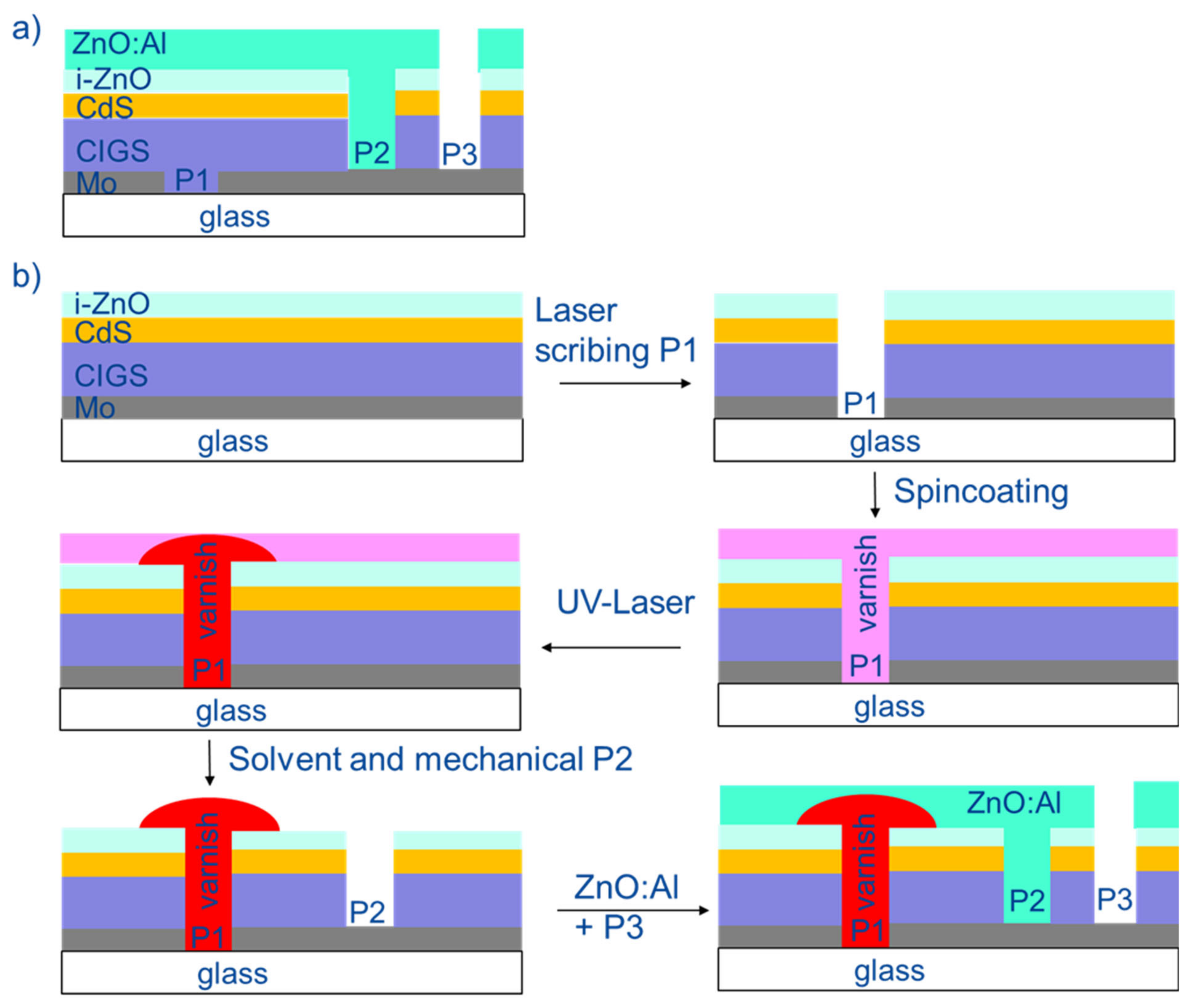
5] extended for modules by monolithic interconnection of cells. The serial interconnection patterning lines P1, P2, and P3 were used, with P1 separating the back contact, P2 establishing the contact between the front contact TCO of one cell to the Mo back contact of the next cell, and P3 isolating the front contact from one cell to the next cell. Two module patterning approaches were investigated. For the standard module design, the molybdenum was laser-scribed for the first pattering line (P1). The next two patterning lines were performed by mechanical scribing with a stylus. The modules on 10 cm × 10 cm substrates consist of 18 cells, each 4 mm wide including a dead area (beginning with P1 up to the end of P3) of 275 µm and a cell length of 84 mm. For modules with filled P1 groove, the P1 laser scribing was performed after deposition of the i-ZnO layer. To fill the P1 groove, a varnish was spin-coated using IUSS06-01LV varnish from inktec-ESC and a Spin Coater (Laurell model WS 400B-6NPP/AS2). The spinning procedure was a dynamic application via a syringe with a pressure of 8.7 psi at 500 rpm for 2.8 s. Further spinning was carried out at 500 rpm for 7 s and finally at 1400 rpm for 20 s. The varnish was cured using a UV laser in the P1 groove. Rinsing in ethylacetate for 10 s removed the residual uncured varnish. This module consists of 19 cells with 4 mm each including a dead area of 420 µm and a cell length of 80 mm (see
Figure 1). The reason for the larger dead area is that the patterning procedure was not optimized in order to ensure good coverage of the P1 groove by the varnish.
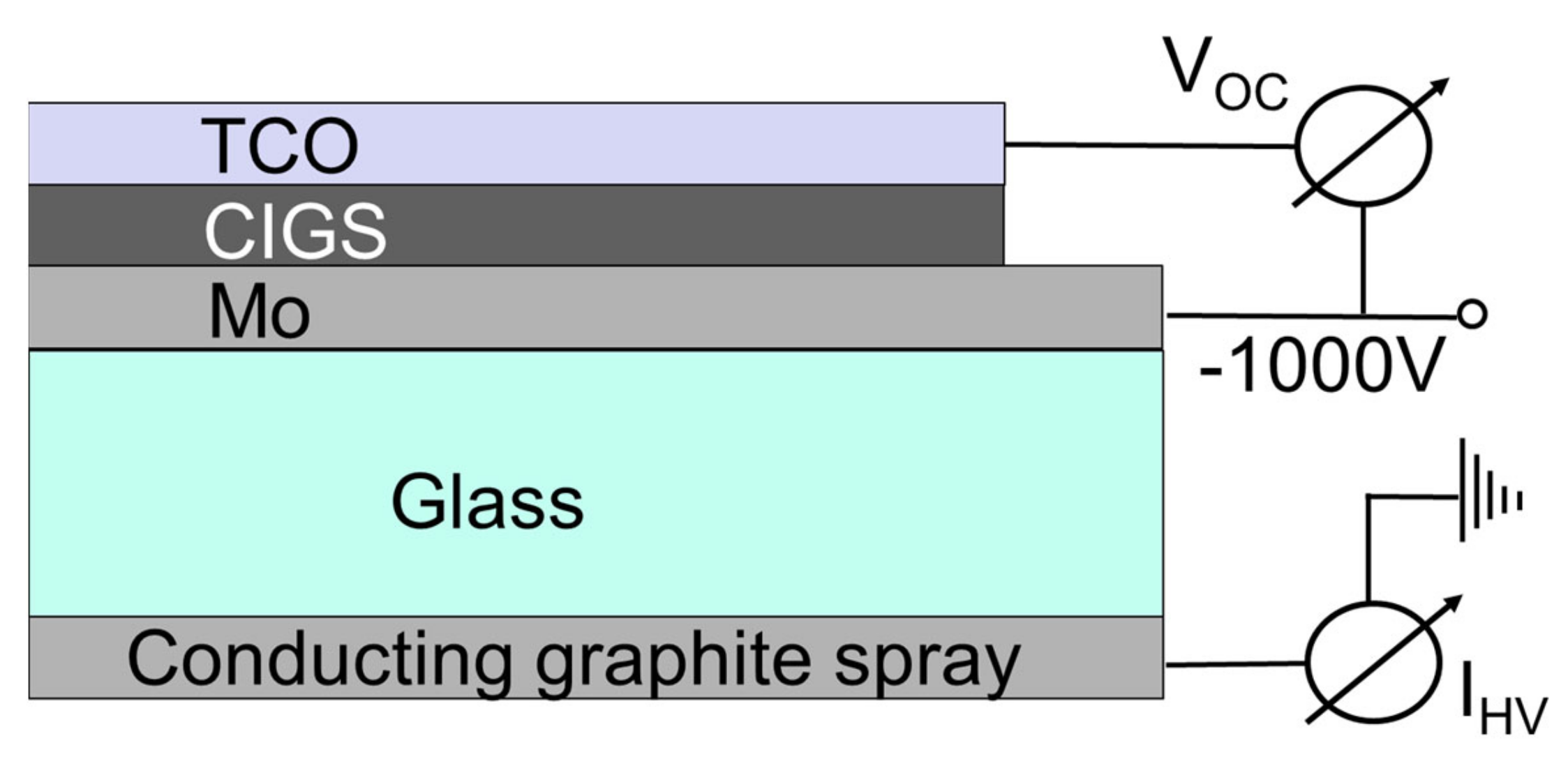
To prevent charge flow over the edges of the glass substrate, a 1 cm laser edge deletion process was employed. Prior to performing PID tests, the samples underwent preparation involving etching the backside up to the sample edges using a 5% HCl solution. This step aimed to eliminate any conductive pathways that might have been created by ZnO or CdS, followed by thorough rinsing with water. Subsequently, the backside of the glass substrate was coated with a conductive graphite varnish (Cramolin GRAPHIT 1281411) only in the region that still contained Mo/CIGS/TCO layers after edge deletion, ensuring uniform voltage distribution.
To establish electrical connections, tinned copper ribbons were affixed to the positive and negative terminals of the module using silver-conductive adhesive, as well as to the graphite layer. The power supply unit responsible for applying a 1000 V positive or negative bias was a FUG type HCP 350-12500MOD. High-voltage current measurements were carried out using IPC2U measuring devices (I-7017).
Humidity plays a significant role in PID, as a moisture film on the glass surface acts as an equipotential surface, enabling current flow through the glass. The leakage current through the glass depends on relative humidity, applied voltage, and module temperature [
8]. To mitigate external influences such as temperature, humidity, and variations in string bias due to changing light conditions, tests were conducted in a Feutron type 3436/15 climate chamber with low humidity set at 10%. The chamber was also maintained at a temperature of 70 °C. A defined high voltage was applied between the positive terminal of the module and the equipotential graphite layer on the backside of the substrate glass to assess the module’s resistance to PID.
Additionally, the current-voltage (I-V) characteristics of CIGS solar cells were measured at 25 °C under simulated AM1.5G illumination at 1000 W/m2 (WACOM WXS-90S-5).
Figure 2 shows a schematic diagram of the layer structure and measurement setup for the CIGS solar cell, which we already used in [
5]. For the modules, the high voltage was applied between the positive pole of the module and the equipotential graphite layer on the backside of the substrate glass for testing the module stability against PID.
3. Results
Two module types, distinguished solely by the patterning procedure but otherwise possessing identical compositions, were subjected to a specified high voltage. This voltage was applied between the conductive graphite substrate on the backside and the Mo back contact of the cell or the positive pole of the module. When the Mo back contact served as the anode (+1000 V), no damage to our cells or modules was observed (not depicted). Moreover, subjecting the modules to charge displacement via AC voltage (250 V) caused no discernible harm, which mirrored the behavior of individual cells.
However, when exposed to a high negative external potential, such as −1000 V (with the Mo back contact acting as the cathode) applied between the Mo and the substrate’s backside, the photovoltaic performance significantly deteriorated after a certain amount of electrical charge passed through the substrate. It is important to note that this effect was observed in the standard module, despite using the PID-resistant cell stack described in our previous publication [
5].
However, the module with a filled P1 exhibited an equally slow degradation behavior as the pure cell. As the open-circuit voltage (V
oc) was the first indicator for cell degradation as reported in [
5], we also exposed the modules to a halogen lamp during HV application to measure the weak-light voltage (V
wl) and thereby had an online indicator for the degradation. As a consequence of this V
oc loss, the fill factor (FF) and the short circuit current (I
sc) degraded too for PID-susceptible modules/cells at higher charge transferred. V
wl was measured every minute.
For comparison, a pure cell was also measured with the same procedure. In the experimental arrangement outlined earlier, conducted within the climate chamber at 70 °C with a humidity level of 10%, the current resulting from the high voltage (−1000 V) remained consistently at approximately 35 nA/cm
2 for the modules on 3 mm soda-lime glass substrates. This measurement closely resembled the results obtained for the cells in our previous publication [
5].
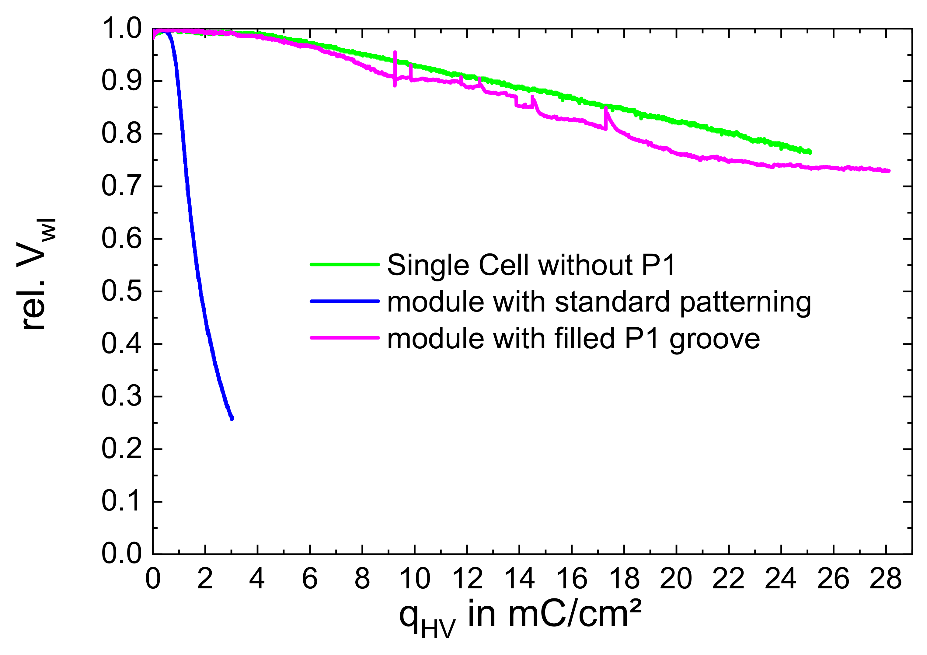
Figure 3 shows the relative V
wl as a function of the transferred HV charge q
HV. The transferred charge was calculated by integrating the measured HV current through the glass over time (as this current was quite constant the charge scale also reflects a time scale). For modules with standard patterning, the V
wl severely drops after only a small amount of transferred charge of 0.5 mC/cm
2 despite the fact that stable cell material was used (blue curve). As indicated by the green curve, the pure cell was stable. For modules with a filled P1 groove, the modules were PID stable and behaved like the pure cell material (magenta curve). A very small degradation starts at 4.5 mC/cm
2, also at a much slower degradation rate. Even after 9 mC/cm
2 of HV charge, the transferred V
wl is still larger than 90% of the starting value. After 9.2, 9.8, 11.7, 12.4, 14.5, and 17.3 mC/cm
2, respectively, for the module with a P1 fill, the climate chamber power source was turned off for several hours to check whether the module regenerated. As during this time no current is transferred, this regeneration effect appears as steps in the curve. However, degradation continues with further application of high potential and, therefore, transferred charge through the substrate glass. The slow degradation for this much more stable module continues in a much slower slope and is shown for HV charges up to 28.2 mC/cm
2 with a degradation down to 75% of the original value.
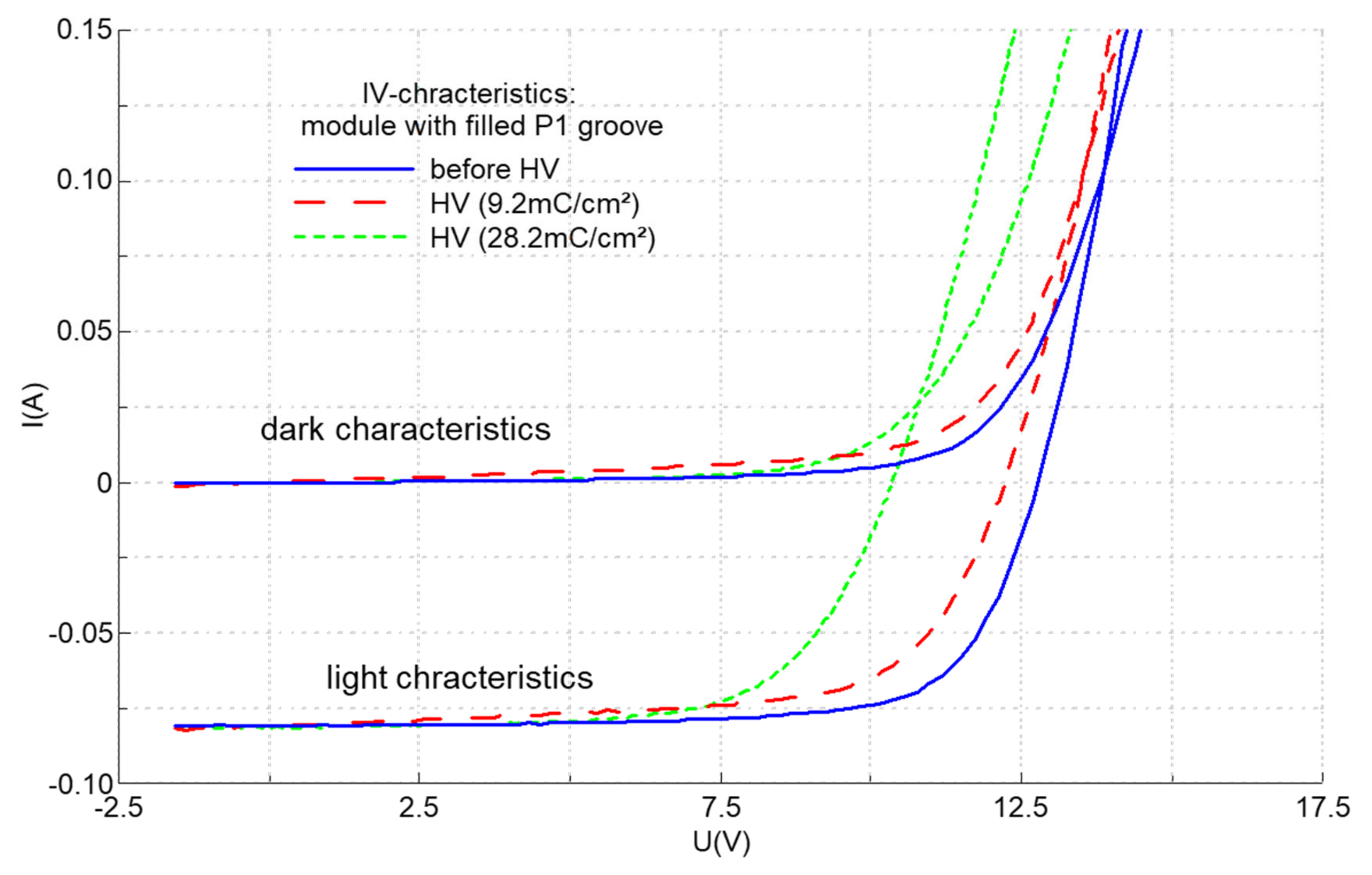
Figure 4 shows the characteristics of the module with a filled P1 groove. After 9.2 mC/cm
2 the Voc and FF just slightly degraded, while the standard module completely degraded (see
Figure 3 blue line).
4. Discussion
We investigated two distinct types of CIGS modules. One exhibited susceptibility to PID when the positive module pole, which was in contact with a tinned copper tape, served as a cathode, despite the stability of the unpatterned individual cell material. The other module demonstrated enhanced resistance to PID. As the PID-susceptible module accumulated a certain amount of charge, it began to degrade. This relationship between charge accumulation and degradation under negative bias was also demonstrated by Lechner et al. in their study on CIGS thin-film modules in the field [
9]. The impact of high negative voltage on the performance of CIGS PV modules is further corroborated by the findings of Boulhidja [
10], Hacke [
11], and Liu et al. [
12].
In contrast, Sakurai et al. reported no discernible effect of negative bias in the field for their tested chalcopyrite-based Cu(In,Ga)(S,Se)2 modules, opting instead for positive bias, which they found to have a more noticeable impact on maximum power changes, if any (within the range of ±2%) [
13]. They also noted that this polarity choice differed from other reported findings.
Weber et al. also confirmed that CIGS modules at the further end of the negative string are most affected as the potential difference between cells and the module frame is maximized at that position [
14]. They confirmed this finding by electroluminescence measurements. It is therefore confirmed in several publications and also in field modules that PID damages CIGS modules. Lechner et al. also give a lifetime estimation for CIGS modules for an estimated failure to 90% power output of the initial value. They correlated the average charge transferred per day from outdoors with the charge needed to degrade the modules to 90% efficiency to calculate the time to transfer this charge. The average charge transferred per day was 1.3 mC/m
2d in southern Germany [
15]. The reference module with standard P1 filling in our indoor experiment degrades down to 90% of the initial value with a charge of 0.95 mC/cm
2 (see
Figure 3), and up to 10 mC/cm
2 is needed for the module with a filled P1 groove. With these numbers, this estimates an average lifetime of 20 years for the standard module or 211 years for the module with a filled P1 groove. This clearly indicates the relevance of the immunization strategy against PID with a filled P1 groove.
Muzillo et al. have identified two distinct PID mechanisms. One is front shunting, which is caused by a high potential (1000 V) to the front glass that results in alkali metal cations gathering in the i-ZnO buffer to increase shunt conductance and slowly reduce the fill factor (FF). And, the other mechanism is p-n junction PID, which is driven by applying a high potential (1000 V) to the back glass which rapidly decreases carrier concentration due to the accumulation of alkali metal cations in particular sodium ions near the junction, where they compensate with majority carriers to reduce the built-in field and V
oc. The cations may also act as shunt paths through the junction to reduce the FF [
16].
Yilmaz et al. [
17,
18] closed the gap between laboratory-made CIGS in-depth microanalyses without encapsulants and front glass sheets that report sodium accumulation within the different layers of CIGS and field modules with glass sheets and encapsulants that only report current–voltage and leakage current measurements. Cells extracted from areas with low electroluminescence show dramatically deteriorated current–voltage characteristics, while reference cells from the brighter parts of the module still perform well. Cells from the areas with low electroluminescence degrade strongly in ambient conditions and Na profiles show large changes compared to the less affected cells. However, no trace of Na was detected in the ZnO layer, which indicates that sodium migration occurs from the substrate glass to the solar cell. Sodium accumulation in the absorber layer degrades the electrical properties of the layers.
Other authors have also investigated the impact of applying a voltage between the front glass of CIGS modules and the cells [
19,
20,
21]. Alonso-Garcia suggests that potential-induced degradation (PID) through the front glass may be significantly less significant compared to that occurring through the rear [
22]. Therefore, the p-n junction PID as described by Muzillo which is driven by a high potential to the back glass seems to be the dominant degradation mechanism.
In this work, strategies to circumvent this degradation mechanism by a filled P1 groove are shown.
Some strategies to circumvent PID were also proposed by Yilmaz et al. in their review of potential-induced degradation [
23]. These strategies are distinguished as follows:
(a) On the system level, PID can be prevented easily by using an inverter structure grounding the negative end of the strings. Further, the mounting system and frame can be modified to reduce leakage currents but this probably does not circumvent the fact that leakage current peaks in the mornings in the presence of morning dew.
(b) On the module level, encapsulants with high electrical resistivity can be used, or glasses with reduced sodium content [
23]. Fjällström et al. [
24] demonstrated that cells on sodium-free glass exhibited no degradation. The alkali-free glass displayed excellent insulating properties, preventing any charge transfer. A similar result was reported by Muzzillo et al. [
25]. They utilized less-conductive potassium-rich borosilicate glass (BSG) substrates, which resulted in a 35-fold reduction in leakage current under high voltage conditions. However, after introducing equal amounts of cations into the devices, both the SLG and BSG substrates in their study exhibited similar performance degradation.
(c) On the cell level, the addition of a barrier or denser molybdenum back contact can increase PID stability. The PID-resistant cells in our experiment remained stable even when subjected to a substantial amount of charge passing through the glass substrate. Similarly, Muzillo et al. [
26] demonstrated CIGS devices that exhibited a significantly longer time to failure (five times longer compared to their standard devices). The improved devices featured an additional Al
2O
3 barrier layer positioned between the soda-lime glass (SLG) and the Mo back contact. Notably, both their reference and Al
2O
3-coated samples showed comparable leakage currents. So, an addition of a barrier or even a molybdenum with a decreased porosity as described in our previous work [
5] leads to an extended stability against PID of more than 10 times compared to samples without a barrier layer.
Sodium accumulation with an associated decrease in doping concentration seems to take a major role in the degradation, which is already shown in different publications [
5,
24,
25,
27] using GDOES or SIMS investigations. An increase in sodium (Na) content, accompanied by a decrease in doping density, appears to contradict earlier findings that suggested high efficiencies could be attained through Na diffusion into the CIGS absorber during the deposition process. The presence of Na in this context has been associated with an enhancement in p-type conductivity, consequently leading to improved Voc (open-circuit voltage) and FF (fill factor) [
28,
29]. However, Champness et al. demonstrated that a type inversion can occur in stoichiometric CuInSe
2 Bridgman crystals when a larger quantity of Na is present [
30]. Therefore, an excessive supply of Na can lead to a decline in cell performance. The depth profile and concentration of Na at the CIGS surface play a crucial role in determining the properties of CIGS solar cells [
31]. For this reason, it appears that sodium accumulation in the absorber is the main driver for the p-n junction PID described by Muzillo et al. [
16].
(d) Finally, another immunization strategy in addition to the review from Yilmaz [
23] specifically for modules, which to our knowledge has not been reported in the literature, is to fill the P1 groove with an insulator material. This probably prevents the above-mentioned sodium migration from the direct contact between the glass and the CIGS absorber and significantly increases the PID stability, as shown by our results.


