Review

Sputtering Process of ScxAl1−xN Thin Films for Ferroelectric Applications

Department of Metallurgical and Materials Engineering, The University of Alabama, Tuscaloosa, AL 35487, USA
*
Author to whom correspondence should be addressed.
Coatings 2023, 13(1), 54; https://doi.org/10.3390/coatings13010054
Submission received: 21 November 2022 / Revised: 10 December 2022 / Accepted: 20 December 2022 / Published: 28 December 2022
(This article belongs to the Special Issue Advances in Thin Film Fabrication by Magnetron Sputtering)

Abstract

:
Several key sputtering parameters for the deposition of ScxAl1−xN such as target design, sputtering atmosphere, sputtering power, and substrate temperature are reviewed in detail. These parameters serve a crucial role in the ability to deposit satisfactory films, achieve the desired stoichiometry, and meet the required film thickness. Additionally, these qualities directly impact the degree of c-axis orientation, grain size, and surface roughness of the deposited films. It is systematically shown that the electric properties of ScxAl1−xN are dependent on the crystal quality of the film. Although it is not possible to conclusively say what the ideal target design, sputtering atmosphere, sputtering power, and substrate temperature should be for all sputtering processes, the goal of this paper is to analyze the impacts of the various sputtering parameters in detail and provide some overarching themes that arise to assist future researchers in the field in quickly tuning their sputtering processes to achieve optimum results.

1. Introduction

The use of piezoelectric thin films has seen a surge in recent years due to its various applications such as in microelectromechanical systems (MEMS), bulk acoustic wave (BAW) resonators, and surface acoustic wave (SAW) resonators to name a few [1]. Traditionally, Aluminum Nitride (AlN) was among one of the most used piezoelectric materials for such applications because it is completely semiconductor compatible and has satisfactory piezoelectric properties [2,3,4]. However, the demand for materials with superior piezoelectric coefficients resulted in the investigation of Sc-doped AlN thin films. In 2009, it was discovered that the partial substitution of aluminum with scandium to form ScxAl1−xN resulted in a substantial increase in the piezoelectric response [5]. The approximately 500% increase in piezoelectric modulus, d33, of ScxAl1−xN when x = 0.43 was ascribed to the phase transition from wurtzite to layered hexagonal with increasing scandium content [5]. Furthermore, it was found that the electromechanical coupling factor, kt2, could be improved from 7% to 10% when x ≤ 0.2 [6]. Due to these excellent piezoelectric characteristics, ScxAl1−xN has garnered substantial interest in the piezoelectric community and is expected to be an ideal candidate for piezoelectric thin-film layers.
More recently in 2019, Fitchner et al., demonstrated the first official instance of ferroelectric switching in ScxAl1−xN [7]. This paramount discovery has generated a resurgence in research related to ScxAl1−xN. High-performance thin-film ferroelectrics exhibiting good technological compatibility with generic semiconductor technology are in urgent demand due to emerging applications based on controlling electrical polarization, multitude of memories, and micro/nano-actuators [7]. Similar to the piezoelectric response observed in ScxAl1−xN, the ferroelectric nature of the material arises as a result of the anisotropic crystal structure that originates from the layered-hexagonal structure when Sc-doping occurs [8]. For this reason, ScxAl1−xN is considered to be a possible candidate for the development of practical two-terminal ferroelectric nonvolatile memory devices (FE-NVMs) [9].
To date, there have been two primary deposition routes used when creating ScxAl1−xN thin films. These include both molecular beam epitaxy (MBE) and RF or magnetron sputtering. Although there are benefits to MBE deposition such as better control over thickness, crystallinity, and stoichiometry, sputtering represents a more viable deposition process because of its relatively low cost, reproducibility, good adhesion with the substrate, ability to deposit stoichiometry of target material, and potential for large-scale manufacturing. However, a systematic review of the sputtering parameters for thin film ScxAl1−xN is absent from the literature.
In this review, the evolution and optimization of the various sputtering parameters for ScxAl1−xN is reported. There are several key parameters during sputtering that have a critical outcome on film properties. For instance, in this review target design, sputtering atmosphere, sputtering power, and substrate temperature will be examined in detail. Deposition parameters such as these will directly affect the deposited film quality, including the thickness and morphology. Many reports have analyzed the effects of one or more of these deposition parameters on such quality indicators as film thickness, crystallinity, or final composition. Moreover, various reports have then connected those film quality indicators to the eventual electric properties of the resulting film. The type of substrate can also play a role in controlling the final crystal quality of the ScxAl1−xN films. Li et al., compared ScAlN films prepared on both silicon and C276 alloy substrates and found that the films prepared on C276 alloy substrates resulted in non-ideal, a-axis oriented ScAlN films. However, films prepared on Si resulted in all c-axis oriented crystals. The non-ideal behavior was attributed to the superior lattice mismatch of the Si substrate [10]. For this reason, most literature reports depositing ScAlN on c-axis oriented substrates such as silicon or sapphire. Thus, since the literature comparing the impacts of different substrates (i.e., amorphous silicon) are scarce this review chooses not to focus on this topic. Specifically, in this review, the goal is to interconnect the findings of all existing reports and generate a better understanding of the sputtering process for ScxAl1−xN.

2. Structure and Properties of ScxAl1−xN

2.1. Structure of ScxAl1−xN

It has long been known that the III-nitride materials, such as AlN, GaN, and InN, possess a wurtzite-type crystal structure (space group P63mc) [11]. Moreover, there is a spontaneous polarization along the c-axis of these III-V semiconductors, which leads to the separation of group-III and nitrogen atoms in individual planes [7]. This phenomenon leads to the piezoelectric response in this class of materials. Moreover, it was discovered that the piezoelectric response of AlN can be significantly increased by forming solid solutions with ScN [5]. While pure ScN has a stable cubic rock salt crystal structure, it also maintains a highly metastable, nearly fivefold coordinated layered-hexagonal phase (space group P63/mmc) [12]. Therefore, the belief in the research community is that there is a transition from pure wurtzite to a more layered-hexagonal crystal structure with increasing scandium content as shown in Figure 1.
Moreover, the metastable hexagonal phase works to flatten the ionic potential landscape, which causes the wurtzite basal plane and the length of metal-nitrogen bonds parallel to the c-axis relative to the lattice parameter, c, to increase [13,14]. In other words, the distance between the (0001) planes that hold both the nitrogen atoms and the metal atoms increases with increasing Sc-content. On account of this, the energy barrier is set to decrease with increasing Sc content, leading to an overall reduction of the energy barrier between the two polarization states of the wurtzite structure and creating an avenue for ferroelectric switching. Furthermore, the wurtzite to layered-hexagonal transition is responsible for both the reciprocal increase in piezoelectric response with increasing Sc content and the ability of ScxAl1−xN films to exhibit ferroelectric switching [7].

2.2. Properties of ScxAl1−xN

A summary of some of the structural, optical, electrical, thermal, piezoelectric, and ferroelectric properties of ScxAl1−xN are reported in Table 1. Since ScxAl1−xN is a ternary alloy with properties that are highly dependent on the Sc content, most of the reported values are presented as a range. Additionally, the equations used to generate the values with respect to Sc content are provided as well.
It is clear from the excellent piezoelectric and ferroelectric properties of ScxAl1−xN that it has tremendous potential for use in various power electronics. Moreover, the excellent piezoelectric properties of ScxAl1−xN and low processing temperature make it a suitable choice for power devices such as surface and bulk acoustic wave resonators [24]. Additionally, the recent discovery of ferroelectricity in low-temperature processed ScxAl1−xN provides substantial opportunities for direct memory integration with logic transistors, providing the possibility for the back-end of the line (BEOL) integration on silicon logic. Thus, taking advantage of high ferroelectric switching and coercive fields, ferroelectric field-effect transistors (FE-FET) can be fabricated [25]. However, in order to maximize the piezoelectric and ferroelectric properties in ScAlN thin films, high-quality thin films must be deposited, which is only possible by utilizing optimum sputtering conditions.

3. Sputtering Process for Scandium Aluminum Nitride

3.1. Deposition Parameters

Reactive sputtering is a physical vapor deposition (PVD) process that utilizes charged ions from a mixture of argon and reactive gases to bombard a target causing the ejection of surface atoms from that target and the eventual deposition of those target atoms onto a substrate following the reaction with the reactive gas. In the case of ScxAl1−xN, the reactive gas is nitrogen (N2). Many different parameters can be altered during the reactive sputtering process to achieve desired deposition outcomes. These include parameters such as target design, sputtering atmosphere, sputtering power/power density, substrate temperature, sputtering time, and target-to-substrate distance. However, the primary parameters that have been focused on and investigated thus far in the literature are target design, sputtering atmosphere, sputtering power/power density, and substrate temperature [6,24,26,27]. Table 2 lists the published articles that deposited c-axis ScAlN films on top of several substrates using a variety of sputtering equipment and processes.

3.2. Target Design

Target design is a crucial step in the sputtering process because it will directly impact both the final film’s stoichiometry and uniformity. Three types of target designs have been widely used for the sputtering of ScxAl1−xN thin films. including alloy sputtering targets, pure metal sputtering targets (used in conjunction with dual co-sputtering), and segmented targets [24]. A schematic representation of the three different target types is illustrated in Figure 2. The final thickness and composition of the ScxAl1−xN film deposited can be controlled in different ways depending on the target chosen. For example, for a dual co-sputtering target the final film composition can be varied by selectively adjusting the power applied to the Sc and Al sources, respectively. Correspondingly, for a Sc-Al alloy target the final film composition can be varied by carefully tuning the alloy composition of the target. Lastly, for Sc-Al segmented targets the distribution, size, and quantity of various Al and Sc segments allows for facile and precise tuning of film composition and homogeneity [24].
Early in the research days of sputtering ScxAl1−xN, the primary sputtering technique was dual co-sputtering [5,27,42,43,44]. However, there was a clear transition from dual co-sputtering, using two pure targets, to the use of Sc-Al alloy targets for sputtering. In fact, approximately 67% of the literature cited the use of alloy targets during the period of 2010 to 2018 [6,7,10,17,24,32,33,34,35,39,45]. The primary reason for this transition was that during this period dual co-sputtering was thought to make it difficult to maintain a consistent scandium concentration in ScxAl1−xN films over large substrates due to the difference in scandium and aluminum sputtering yields [45]. Additionally, single-target sputtering is more attractive for industrial high-volume production because it has a higher deposition rate [35].
Although single-alloy target sputtering has several advantages, it is confined by its lack of tunability of the Sc concentration. Thus, as interest grew to develop ScxAl1−xN films with ever increasing Sc content, the preferred deposition mode again pivoted towards dual co-sputtering. Dual co-sputtering is unique in that the Sc concentration can be set directly by tuning the two powers of the sputtering targets [35]. In Table 3, the transition between different sputtering targets is made especially clear, as is the correlation with the desired ScxAl1−xN composition. In general, it can be stated that single-alloy-target sputtering is best suited for the deposition of ScxAl1−xN films with x 0.3 and dual co-sputtering is better suited for handling deposition of compositions where x > 0.3 and precise control over chemistry is required.
In recent years, there has also been the introduction of a third class of sputtering targets known as a segmented targeted. The primary advantages and disadvantages of Sc-Al alloy targets and dual co-sputtering targets are compared in table IV. Sc-Al alloy targets allow for higher deposition rates, which make them well suited for use in industrial applications. Additionally, the alloy target provides consistent Sc content across large substrate areas. However, this target design is very expensive to produce due to the complicated metallurgy required to produce it. Moreover, the alloy design makes quick tuning of the final films Sc content very difficult. On the other hand, using two pure Al and Sc targets in a dual co-sputtering setup allows for facile tuning of Sc content by tuning the power on the respective targets. Additionally, this setup significantly reduces the cost of the targets due to its simple nature. Yet, the dual co-sputtering target design only allows for residual stress tailoring by altering the reactive gas flow, which ultimately degrades film uniformity and crystallinity. Additionally, this design makes it difficult to obtain final films with tensile stress. Thus, Sc-Al segmented targets were developed to overcome the disadvantages of the two prior methods while maintaining as many of the advantages of them as possible. A comparison of the various target designs is presented in Table 4. By combining alternating segments of Sc and Al as shown in Figure 2c, it was possible to get a more uniform distribution of Sc in the ScxAl1−xN films [24]. Additionally, the segmented target design allowed for a significant reduction in film thickness while maintaining excellent control over Sc content and residual film stress [8]. Furthermore, achieving thin films of such thicknesses was especially beneficial for use in ferroelectrics.
Although few papers have been published that explicitly compare ScxAl1−xN deposition with different targets, the target design remains one of the most crucial sputtering parameters [24,35]. In fact, there remains more opportunities to investigate novel modifications to target design and setup. For instance, Posadowski et al., explored the critical role that the placement of substrates versus the target axis, i.e., the so called on- or off-axis mode, had on the properties of deposited films of AlxZnyO when using a two element segmented target [46]. During the engineering of the electric properties of piezoelectric and ferroelectric materials such as ScxAl1−xN, it is vital to achieving desired material stoichiometry [40]. Furthermore, choosing the correct target to achieve the desired chemistry and electric properties is of paramount importance and must not be understated.

3.3. Sputtering Atmosphere

A second critical reactive sputtering parameter that must be taken into consideration is the sputtering atmosphere. Sputtering atmosphere consists of both the chamber pressure and the proportion of argon to nitrogen gas [6]. There have been several studies conducted that examine how the variation in sputtering atmosphere affects parameters such as crystal quality, sputtering rate, residual stress, and the electric properties of the film [6,28,34,36,39]. Because sputtering atmosphere is one of the parameters that directly impacts the energy for adatoms to bombard the surface of the substrate, it is especially pertinent to optimize the sputtering atmosphere to achieve desired film quality and the subsequent electric properties [47].

3.3.1. Sputtering Pressure

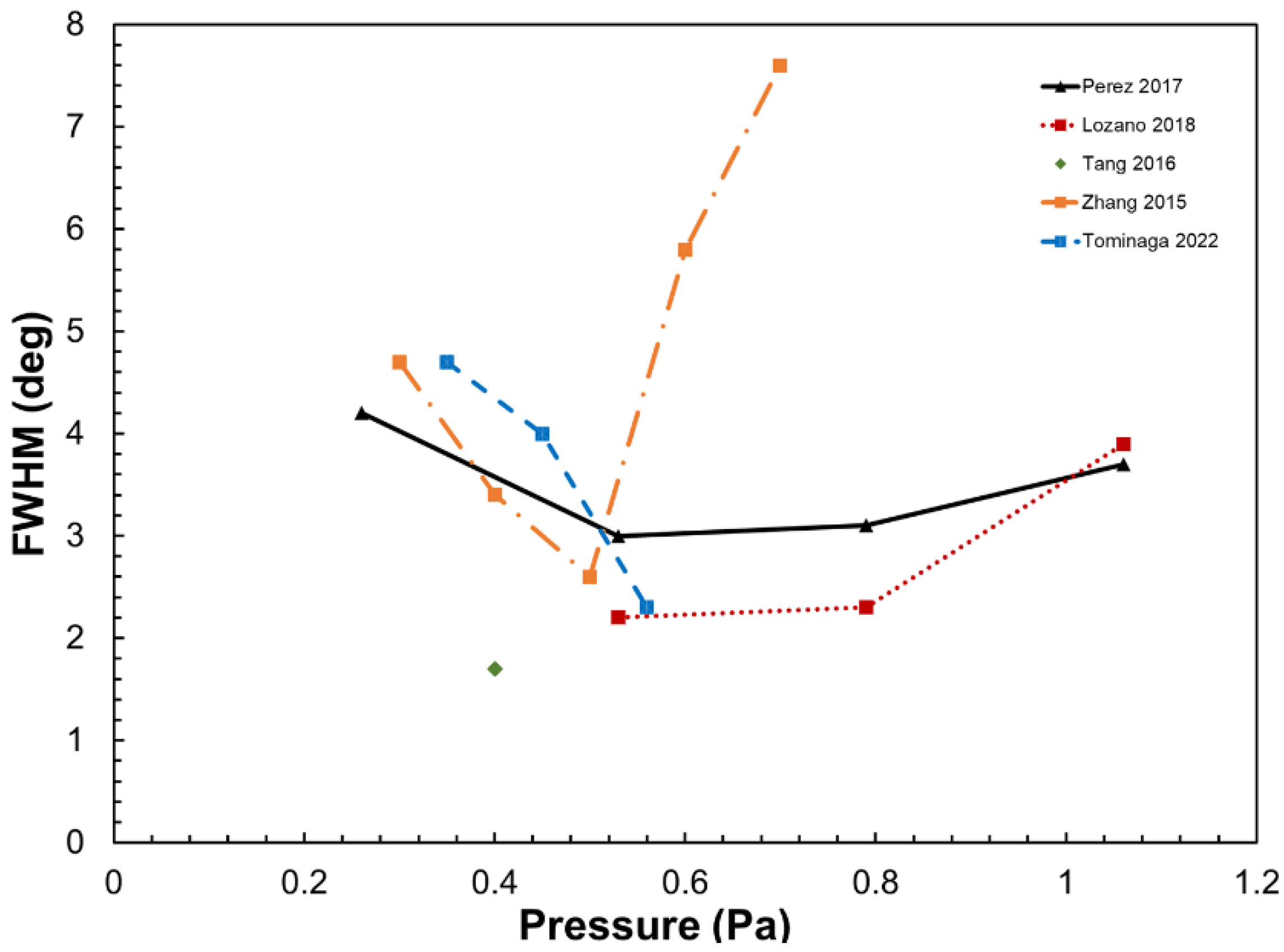
(a) Effect on Crystal Quality: Sputtering working pressure is well known to have a significant impact on the crystal quality of deposited ScxAl1−xN films. Numerous researchers have demonstrated that the highest level of c-axis orientation of ScxAl1−xN corresponds to the lowest full width half maximum (FWHM) of the (0002) peak [36]. Furthermore, when comparing the FWHM values of the rocking curve vs. pressure from several sources, as shown in Figure 3, there appears to be a relative congruence in the ideal pressure for ScxAl1−xN sputtering. Most of the papers reported the lowest FWHM value at an approximate pressure between 0.4 Pa and 0.6 Pa. Additionally, these studies also highlight that the preferred c-axis texture deteriorates at both extremely high and low pressures. In 2022, Tominaga et al., proposed a possible explanation for the deterioration of crystallinity and even electric properties at low-pressure depositions. In short, the report claims that negative-ion bombardment will increase both in quantity and energy at lower pressures, which will negatively impact ScxAl1−xN crystal growth and cause substantial film quality reduction [29].
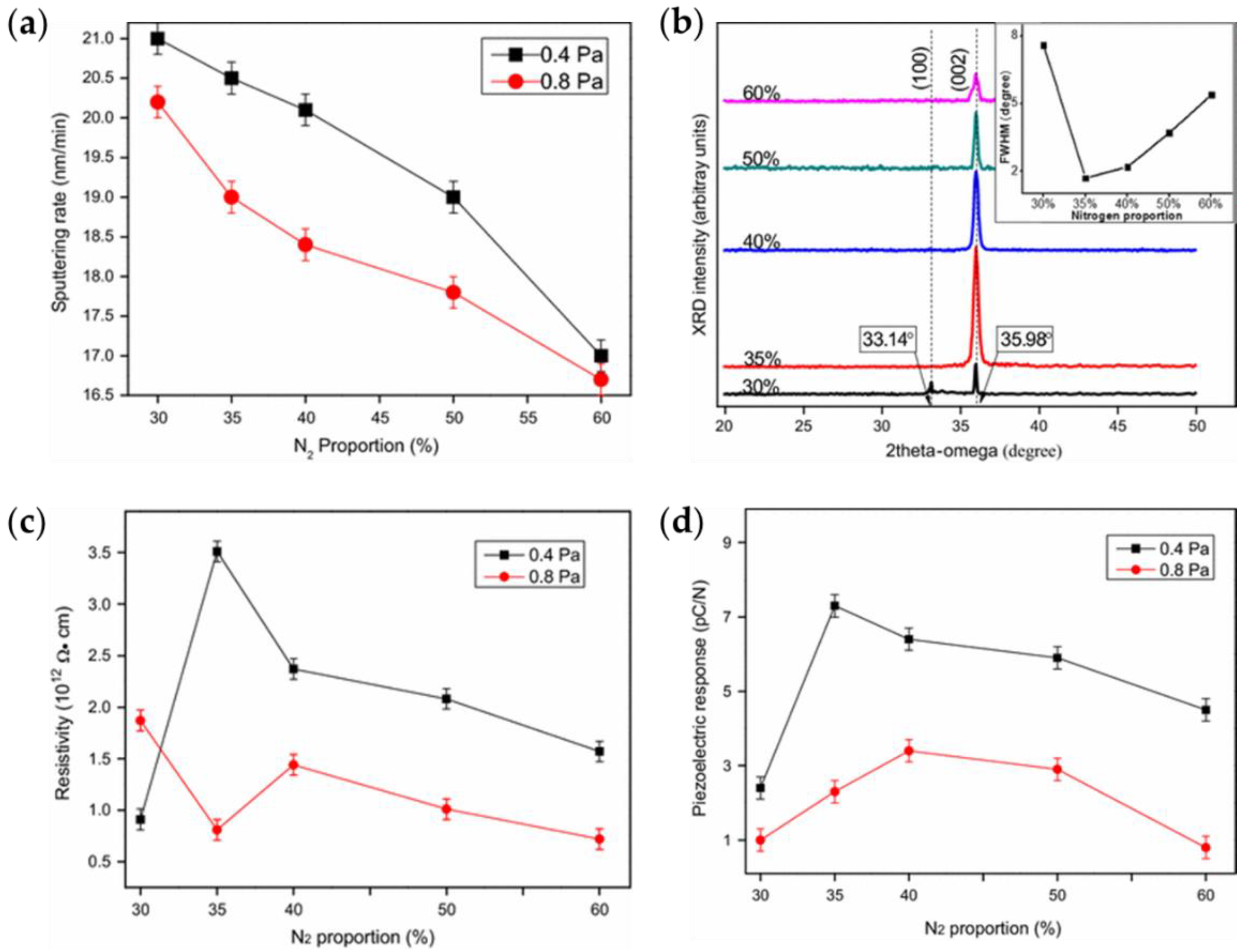
(b) Effect on Sputter Deposition Rate: The impact of sputtering pressure on the sputter deposition rate is partially obfuscated when comparing reports from existing literature related to the reactive sputtering of ScxAl1−xN. For instance, Tang et al., reported that there was a decrease in the sputtering rate with an increase in pressure from 0.4 Pa to 0.8 Pa which was attributed to more scattering between the ejected atoms and the gas atoms, which reduced the mean free path of the ejected atoms [6]. On the other hand, Perez and Lozano reported, respectively, that during deposition at low pressures the rate decreases due to the lower quantity of ions available in the plasma to eject the target material [34,36]. Regardless of these competing theories, the actual deviation of the sputtering rate reported due to the change in pressure is rather minor when compared to the deviation of the sputtering rate due to other parameters such as the sputtering power or N2 proportion. For this reason, more focus should be placed on tuning parameters such as those when seeking control over the sputtering rate of ScxAl1−xN.
(c) Effect on Electric Properties: Resistivity is an important benchmark when comparing piezoelectric thin films. It stands as a crucial indicator of a piezoelectric thin-films ability to achieve both reduced dielectric losses and lower insertion losses when used in electronic devices such as SAW resonators [6,39]. It is well known that a film’s crystallinity directly impacts its dielectric properties. Thus, the pressure that provides the optimum c-axis orientation in the case of ScxAl1−xN should also be the pressure that generates the greatest resistivity. In reality, this theory stands true as is supported by the literature. Tang et al., claim that this occurs because non-ideal sputtering pressure leads to incomplete crystallization, which will ultimately lead to a reduction in resistivity of ScxAl1−xN thin-films [6].
Similar to the resistivity of piezoelectric thin films, the piezoelectric response, d33, is directly impacted by the film’s crystal quality. The trends for rocking curve FWHM values for different sputtering pressures coincide with the trends for the piezoelectric constant (d33) at different sputtering pressures [34]. For this reason, there is a consensus in the literature that the ideal piezoelectric response is achieved when the greatest degree of c-axis texturing occurs [6,28,34,36,39]. Furthermore, by optimizing the sputtering pressure to reach the maximum c-axis orientation, the greatest piezoelectric response can be achieved, paving the way for the creation of piezoelectric sensors and SAW devices [39].
Currently, limited published investigations regarding the effect of sputtering pressure on the ferroelectric response of ScxAl1−xN. However, it can be assumed that the ferroelectric properties of ScxAl1−xN would be tied to the film crystallinity just as the piezoelectric properties were. Since most ferroelectric ScxAl1−xN films are significantly thinner than their piezoelectric counterparts, there is a potential for differences to exist in the ideal sputtering pressure in each case. Regardless, this knowledge gap provides an opportunity for additional research and discovery and warrants further investigation in the future.

3.3.2. Gas Flow Ratio

The gas flow ratio is the ratio of inert gas (Ar) to reactive gas (N2) that is in the sputtering atmosphere during reactive sputtering. The gas flow ratio plays a crucial role during the reactive sputtering process because it controls the amount of reactive gas that is involved during thin film deposition. As shown in Figure 4, deposition parameters such as sputtering rate, structural properties such as crystallinity and surface morphology, and electronic properties such as the resistivity, the dielectric constant, and the piezoelectric response are all greatly impacted and controlled according to the ratio of gas flows [6]. In other words, tuning the concentration of N2 gas present during sputtering is a crucial parameter that must be considered during the reactive sputtering of ScxAl1−xN.
(a) Effect on Sputtering Rate: The effects of gas flow ratio on the sputtering rate of ScxAl1−xN have been shown to exhibit similar trends to those of the AlN system, where sputtering rate decreases with an increasing proportion of N2 gas [48]. The deleterious effect of the N2 proportion on the sputtering rate is clearly demonstrated in Figure 4a. Moreover, Tang et al., explained that there are two possible explanations for this phenomenon. The first explanation is that pure Ar+ ions in the working gas have a higher sputtering yield than N+ or N2+ ions due to their higher mass. The second explanation is related to target poisoning, which occurs with an increasing proportion of N2 [6]. For these reasons, it is very important to be aware of the impacts of the gas flow ratio on the sputtering rate of ScxAl1−xN.
(b) Effect on Crystal Quality: It has been established that excellent c-axis orientation is a prerequisite for achieving maximum piezoelectric or ferroelectric properties in ScxAl1−xN thin-films [38]. Thus, when developing the reactive sputtering procedures for ScxAl1−xN thin-films, it was vital to screen the gas flow ratios to determine the ideal percentage of N2 gas necessary to achieve maximum c-axis orientation. Moreover, it was determined from the literature that the XRD intensity and FWHM of the rocking curves for the (0002) plane are both closely tied to the concentration of N2 [6,39]. At approximately 32%–35% N2, both the XRD intensity for the (0002) plane and the FWHM were found to be optimized as shown in Figure 4b. There is a clear consensus that an atmosphere oversaturated with N2 will lead to “target poisoning” due to excessive N2 reacting on top of the target [39]. On the other hand, an atmosphere undersaturated with N2 will develop poor crystallinity and film quality due to the formation of N-vacancies and Al-interstitials [6]. For this reason, there must be strict control and optimization of the gas flow ratios to ensure proper film quality and crystallographic orientation during the reactive sputtering ScxAl1−xN.
(c) Effect on Surface Roughness: Surface roughness becomes especially important when considering the applications of ScxAl1−xN thin-films such as in SAW devices. Surface acoustic waves are propagated only on the surface, and all the energy is approximately contained in a wavelength from surface to inside [49,50]. Furthermore, SAWs will be critically hindered when the surface roughness of the film is greater than the wavelength. Therefore, it is beneficial to minimize the RMS of ScxAl1−xN films to achieve reduced insertion losses for SAW devices [51]. It has been discovered that the gas flow ratio also has an important impact on the surface roughness of ScxAl1−xN [39]. By optimizing the gas flow ratio to achieve the desired c-axis orientation, it has been shown to minimize the surface roughness [6,39].
(d) Effect on Electric Properties: As mentioned in the previous sections regarding the resistivity and piezoelectric response of ScxAl1−xN films with respect to the sputtering pressure, both parameters are directly dictated by the degree of c-axis orientation of the film. Thus, by optimizing the gas flow ratio to achieve the maximum c-axis orientation, both the highest resistivity and largest piezoelectric response can be achieved. As is shown in Figure 4c,d, the resistivity, piezoelectric response, and dielectric constant are all shown to improve initially with the increasing N2 concentration. However, they show significant degradation after reaching a saturation point [6]. Thus, a harmonious proportion of N2 is required to achieve films with uniform size and minimized defects, which will ultimately lead to the greatest improvement of electric properties.

3.4. Sputtering Power Density

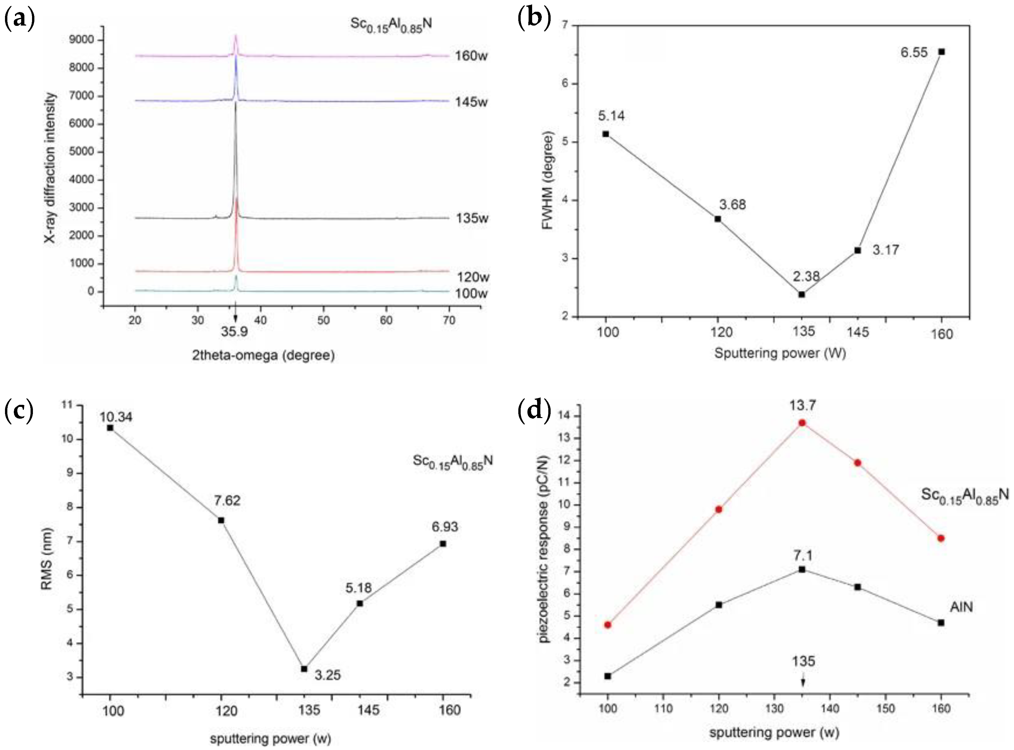
The sputtering power/power density is an additional parameter that is critical to the thin-film deposition of ScxAl1−xN. At the beginning, it was established that the sputtering power significantly influences the deposition of AlN films, affecting both its crystallinity and its electric properties [52]. Similarly, it was discovered that sputtering power plays an analogous role in the thin-film deposition of ScxAl1−xN as is shown in Figure 5 [26].
(a) Effect on Sputtering Rate and Thickness: Sputtering power density becomes especially important during the process of reactive dual co-sputtering of ScxAl1−xN because the variation in power density between the Sc and Al targets allows for the precise control over the concentration of Sc in the alloy [42]. By maintaining a constant power density on the Al target, the Sc concentration can be increased linearly by gradually increasing power density applied to the Sc target [31]. On account of this, most papers employing a dual co-sputtering setup for ScxAl1−xN tend to modulate the power density only as a means to dictate the final stoichiometry of the film. The mechanism governing the linear increase in Sc content with increasing power density is closely related to the mechanism governing the effect of the power density on both the sputtering rate and the film thickness.
Moreover, increased power density generally results in an increase in the sputtering rate of ScxAl1−xN. This can be mainly attributed to the increase in the kinetic energy of the adatoms arriving at the substrate [36]. However, there have been reports of exceedingly high power densities leading to a reduction in sputtering rate due to the occurrence of re-sputtering [10]. Furthermore, since the thickness is a rate-dependent property, it follows the same trend as the sputtering rate for a constant sputtering time. This means that the thickness of sputtered ScxAl1−xN can be systematically tailored by increasing or decreasing the sputtering power for a given sputtering time. Thickness tuning via power density modulation is primarily reserved for cases in which Sc-Al alloys are utilized as the target.
(b) Effect on Crystal Quality: As previously discussed, ScxAl1−xN has a wurtzite structure. As a result of this crystal structure, the (0002) plane has the lowest surface energy because it is the closest packed plane [10]. Additionally, it has been established that with increasing power density, there is an increase in the kinetic energy of Sc adatoms. This helps to promote the rearrangement of atoms to align according to (0002) crystal orientation on the substrate surface, which will contribute to a reduction in surface energy [26]. However, at exceedingly high discharge powers/power densities, the adatoms can harbor an overabundance of kinetic energy that forces the B2 bonds in wurtzite to disassociate, causing crystal quality deterioration [31]. Correspondingly, it has been stated that at higher discharge powers the increase of adatom mobility not only improves the crystal quality, but it is also beneficial in preventing the incorporation of impurities from the background gas [34]. Indeed, these phenomena are widely observable in the data available in the literature where the XRD patterns of ScxAl1−xN and plots of the rocking curve FWHM are shown to improve initially with increasing power density, and then degrade at higher power densities [10,26,31]. An example of this is shown in Figure 5a,b. Moreover, Henry et al., showed that increasing RF power from 80 to 120 W leads to a significant reduction in both compressive stress and the inclusion number, where the inclusion number is the number of non-c-axis orientated grains [33].
Additionally, the surface morphology of ScxAl1−xN films is similarly tied to the sputtering power used during film deposition as the surface properties are improved with increasing c-axis orientation due to the increase in sputtering power. With insufficient power, the film is unable to properly form the desired texture. On the contrary, with increasing power, the mobility of the atoms improves, providing the opportunity to eliminate defects such as inclusions [53]. However, Tang et al., warn that when the power density is increased toward the extreme, the surface of the film is more susceptible to cracking due to thermal stresses [26]. This is reflected in the measured RMS as shown in Figure 5c.
(c) Effect on Electric Properties: The electric properties of ScxAl1−xN such as resistivity, leakage current, and piezoelectric response are closely tied to the crystal quality of the deposited film. With better crystal quality, there are fewer defects in the lattice, which serves an advantageous role in the enhancement of electrical properties [10]. Moreover, when the optimum power condition is chosen such that there is a coincidence between the best crystal quality and surface morphology, the maximum piezoelectric response is achieved [26]. When this occurs, the literature has shown that ScxAl1−xN thin-films are capable of achieving a piezoelectric response at least 250% greater than that of AlN [31].

3.5. Sputtering Substrate Temperature

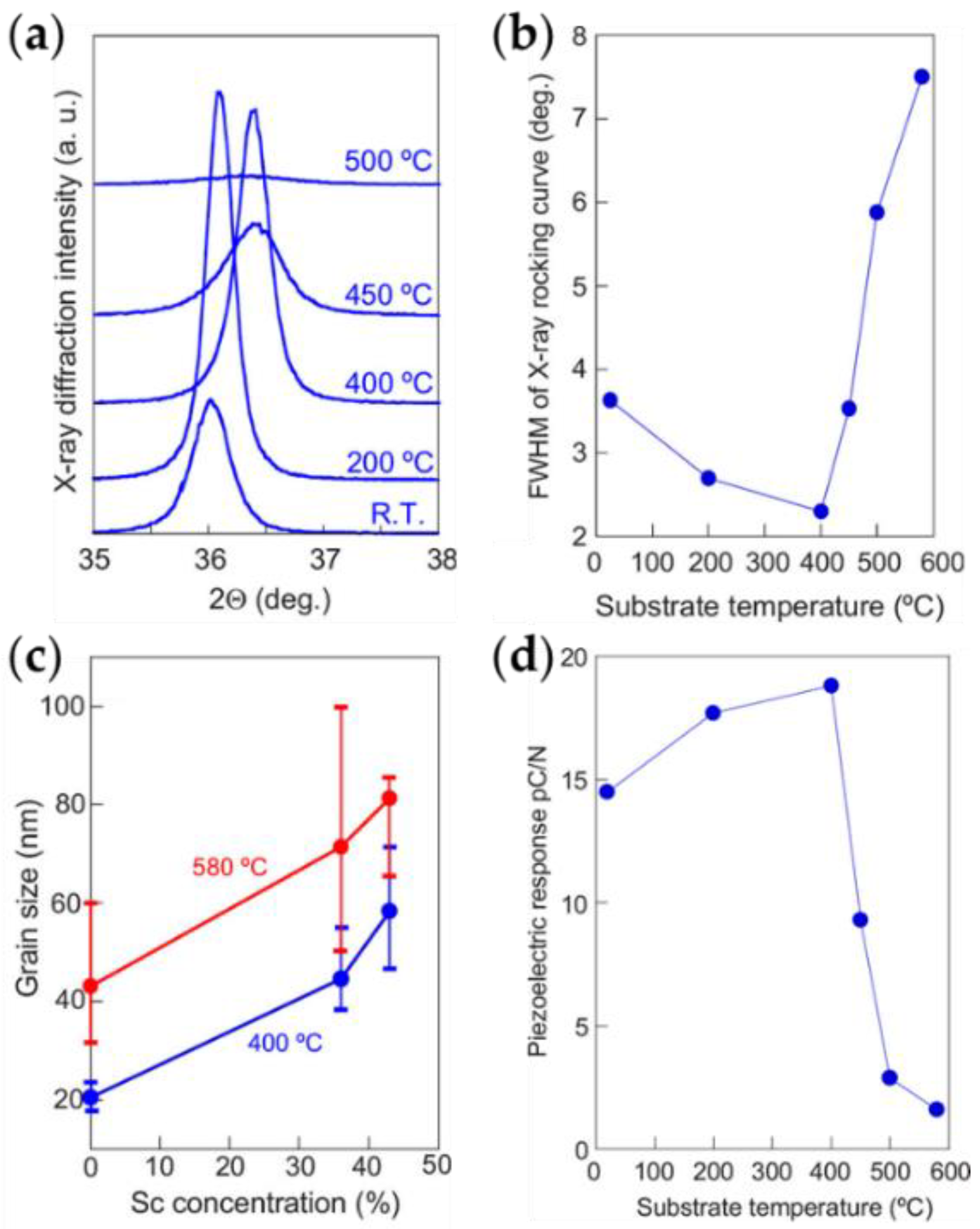
The substrate temperature is a very important parameter to consider during the sputtering of ScxAl1−xN films as it impacts the crystal quality, grain size, and even the final electric properties of the film as shown in Figure 6 [27]. Additionally, the substrate temperature can directly limit what applications the film can be used for. For example, a perquisite for using ScxAl1−xN thin-films in complementary metal-oxide-semiconductor (CMOS)-integrated devices such as ferroelectric field effect transistors (FE-FETs) and random-access memories (RAMs) is a low-temperature (T < 400 °C) deposition [25,30]. Moreover, the low temperature deposition of ScxAl1−xN thin films could alleviate the process integration failures commonly associated with PZT FE-RAMs that require deposition temperatures exceeding 600 °C, which are detrimental for CMOS transistors [8,23].
(a) Effect on Crystal Quality, Grain Size, and Film Stress: It has long been acknowledged that the crystal quality and grain size of ScxAl1−xN films share a dependency with the substrate or growth temperature [5,27,41]. In 2009, Akiyama et al., showed that there was a significant decrease in the crystal quality of films deposited above 400 °C as shown in Figure 6 [27]. Additionally, this decrease in crystal quality was proposed to be the result of a drastic increase in the size and disorder of grains when the growth temperature exceeded 400 °C. Moreover, Zukauskaite et al., showed that at high growth temperatures above 400 °C and higher Sc concentrations, there was a structural degradation into Al-rich and Sc-rich domains, which most likely contributed to the reduction in crystal quality [41]. Likewise, it was found that the number of non-c-axis oriented grains decreases with increasing substrate temperature up to 375 °C before increasing again with subsequent temperature increase [33]. On account of these investigations, the vast majority of literature utilizes a sputtering temperature that is less than or equal to 400 °C.
(b) Effect on Electric Properties: As mentioned in the previous section, the crystal quality of ScxAl1−xN films deteriorates significantly when the substrate temperature exceeds 400 °C. Since the electrical properties of the film are dependent on the crystal quality, this means that they too should degrade after surpassing the temperature threshold. Indeed, this is supported by the data presented in the literature. When Tsubstrate > 400 °C, there is a significant increase in the leakage current [41]. Additionally, the piezoelectric response was shown to drop off drastically when Tsubstrate > 400 °C as shown in Figure 6d [27]. The degradation of the electric properties such as piezoelectric response could also be linked to the formation of Al-rich and Sc-rich clusters, which occurs at higher temperatures [22]. To conclude, it is vital to minimize the substrate temperature during the deposition of thin-film ScxAl1−xN because exceeding the threshold temperature of approximately 400 °C leads to a significant reduction in crystal quality and electric properties while also excluding the film from being easily integrated into CMOS devices.

4. Conclusions

In summary, key sputtering parameters for the deposition of ScxAl1−xN such as target design, sputtering atmosphere, sputtering power, and substrate temperature are vital for depositing high-quality thin films, achieving desired stoichiometry, and meeting the required film thickness. Moreover, this review has shown that these qualities directly impact the degree of c-axis orientation, grain size, and surface roughness of the deposited films. Additionally, the electric properties of ScxAl1−xN films share a clear dependence on the crystal quality of the film. It should be stated that there is no one set of sputtering parameters that is ideal for all applications. Therefore, it is impossible to say definitively what the ideal target design, sputtering atmosphere, sputtering power, and substrate temperature should be. However, some overarching truths can be gleaned from the review of current literature on the sputtering of ScxAl1−xN. These are as follows:
(1)
Sputtering target design is essential to ensure the Sc and Al composition in the ScxAl1−xN films. In general, single-alloy targets appear to be better when depositing films with Sc concentrations less than 30%, whereas dual co-sputtering targets are better suited for applications where concentrations exceed 30% and when the precise control of Sc content is necessary. Lastly, segmented targets are interesting in the ability to combine the advantages of both single-alloy targets and dual co-sputtering targets, but they are less applicable for industrial applications.
(2)
In general, sputtering pressures should be kept between 0.4–0.6 Pa to avoid the issues associated with extremely low or high pressures. Moreover, the gas flow ratio should be kept such that there is between 30% and 35% N2 present.
(3)
Increased sputtering power can benefit the crystal quality and electric properties of ScxAl1−xN. However, there exists a maximum power density whereupon further increase the film quality will become damaged.
(4)
Substrate temperature should not exceed 400 °C during the deposition of ScxAl1−xN.
These insights and this comprehensive analysis can serve as reference points for any novel research project utilizing the sputtering of ScxAl1−xN thin films. Moreover, by utilizing this review future researchers should be able to quickly tune and adjust their sputtering processes to rapidly obtain exceptional results.

Author Contributions

J.M.W. writing—original draft preparation, F.Y.; writing—review and editing. All authors have read and agreed to the published version of the manuscript.

Funding

This work is supported by National Science Foundation under contracts No. ECCS-1944374, CMMI-2019473 and DMR-2127640, National Aeronautics and Space Administration, Alabama EPSCoR International Space Station Flight Opportunity program (contract# 80NSSC20M0141), and USDA National Institute of Food and Agriculture, AFRI project award (contract# 2020-67022-31376).

Institutional Review Board Statement

Not applicable.

Informed Consent Statement

Not applicable.

Data Availability Statement

Not applicable.

Conflicts of Interest

The authors declare no conflict of interest.

References

  1. Piazza, G.; Felmetsger, V.; Muralt, P.; Olsson, R.H., III; Ruby, R. Piezoelectric aluminum nitride thin films for microelectromechanical systems. MRS Bull. 2012, 37, 1051–1061. [Google Scholar] [CrossRef] [Green Version]
  2. Elfrink, R.; Kamel, T.M.; Goedbloed, M.; Matova, S.; Hohlfeld, D.; Van Andel, Y.; Van Schaijk, R. Vibration energy harvesting with aluminum nitride-based piezoelectric devices. J. Micromech. Microeng. 2009, 19, 094005. [Google Scholar] [CrossRef] [Green Version]
  3. Stoppel, F.; Schröder, C.; Senger, F.; Wagner, B.; Benecke, W. AlN-based piezoelectric micropower generator for low ambient vibration energy harvesting. Procedia Eng. 2011, 25, 721–724. [Google Scholar] [CrossRef]
  4. Lu, Y.; Heidari, A.; Horsley, D. A High Fill-Factor Annular Array of High Frequency Piezoelectric Micromachined Ultrasonic Transducers. J. Microelectromech. Syst. 2015, 24, 904–913. [Google Scholar] [CrossRef]
  5. Akiyama, M.; Kamohara, T.; Kano, K.; Teshigahara, A.; Takeuchi, Y.; Kawahara, N. Enhancement of Piezoelectric Response in Scandium Aluminum Nitride Alloy Thin Films Prepared by Dual Reactive Cosputtering. Adv. Mater. 2009, 21, 593–596. [Google Scholar] [CrossRef] [PubMed]
  6. Tang, J.; Niu, D.; Yang, Y.; Zhou, D.; Yang, C. Preparation of ScAlN films as a function of sputtering atmosphere. J. Mater. Sci. Mater. Electron. 2016, 27, 4788–4793. [Google Scholar] [CrossRef]
  7. Fichtner, S.; Wolff, N.; Lofink, F.; Kienle, L.; Wagner, B. AlScN: A III–V semiconductor based ferroelectric. J. Appl. Phys. 2019, 125, 114103. [Google Scholar] [CrossRef]
  8. Rassay, S.; Hakim, F.; Li, C.; Forgey, C.; Choudhary, N.; Tabrizian, R. A Segmented-Target Sputtering Process for Growth of Sub-50 nm Ferroelectric Scandium–Aluminum–Nitride Films with Composition and Stress Tuning. Phys. Status Solidi (RRL) Rapid Res. Lett. 2021, 15, 2100087. [Google Scholar] [CrossRef]
  9. Liu, X.; Zheng, J.; Wang, D.; Musavigharavi, P.; Stach, E.A.; Olsson, R., III; Jariwala, D. Aluminum scandium nitride-based metal–ferroelectric–metal diode memory devices with high on/off ratios. Appl. Phys. Lett. 2021, 118, 202901. [Google Scholar] [CrossRef]
  10. Li, X.; Yang, Y.; Zhou, D.; Yang, C.; Feng, F.; Yang, J.; Hu, Q. Preparation of ScAlN films as a function of power density on Si and flexible substrate by dc reactive magnetron sputtering. J. Mater. Sci. Mater. Electron. 2016, 27, 171–176. [Google Scholar] [CrossRef]
  11. Zoroddu, A.; Bernardini, F.; Ruggerone, P.; Fiorentini, V. First-principles prediction of structure, energetics, formation enthalpy, elastic constants, polarization, and piezoelectric constants of AlN, GaN, and InN: Comparison of local and gradient-corrected density-functional theory. Phys. Rev. B 2001, 64, 045208. [Google Scholar] [CrossRef] [Green Version]
  12. Tasnádi, F.; Alling, B.; Höglund, C.; Wingqvist, G.; Birch, J.; Hultman, L.; Abrikosov, I.A. Origin of the anomalous piezoelectric response in wurtzite ScxAl1−xN alloys. Phys. Rev. Lett. 2010, 104, 137601. [Google Scholar] [CrossRef] [PubMed] [Green Version]
  13. Zhang, S.; Holec, D.; Fu, W.Y.; Humphreys, C.J.; Moram, M.A. Tunable optoelectronic and ferroelectric properties in Sc-based III-nitrides. J. Appl. Phys. 2013, 114, 133510. [Google Scholar] [CrossRef] [Green Version]
  14. Deng, R.; Jiang, K.; Gall, D. Optical phonon modes in Al1−xScxN. J. Appl. Phys. 2014, 115, 013506. [Google Scholar] [CrossRef]
  15. Ambacher, O.; Christian, B.; Feil, N.; Urban, D.F.; Elsässer, C.; Prescher, M.; Kirste, L. Wurtzite ScAlN, InAlN, and GaAlN crystals, a comparison of structural, elastic, dielectric, and piezoelectric properties. J. Appl. Phys. 2021, 130, 045102. [Google Scholar] [CrossRef]
  16. Lu, Y.; Reusch, M.; Kurz, N.; Ding, A.; Christoph, T.; Prescher, M.; Kirste, L.; Ambacher, O.; Žukauskaitė, A. Elastic modulus and coefficient of thermal expansion of piezoelectric Al1−xScxN (up to x = 0.41) thin films. APL Mater. 2018, 6, 076105. [Google Scholar] [CrossRef] [Green Version]
  17. Zhang, Q.; Chen, M.; Liu, H.; Zhao, X.; Qin, X.; Wang, F.; Tang, Y.; Yeoh, K.H.; Chew, K.H.; Sun, X. Deposition, Characterization, and Modeling of Scandium-Doped Aluminum Nitride Thin Film for Piezoelectric Devices. Materials 2021, 14, 6437. [Google Scholar] [CrossRef] [PubMed]
  18. Fu, H.; Goodrich, J.C.; Ogidi-Ekoko, O.; Tansu, N. Power electronics figure-of-merit of ScAlN. Appl. Phys. Lett. 2021, 119, 072101. [Google Scholar] [CrossRef]
  19. Saada, S.; Lakel, S.; Almi, K. Optical, electronic and elastic properties of ScAlN alloys in WZ and ZB phases: Prospective material for optoelectronics and solar cell applications. Superlattices Microstruct. 2017, 109, 915–926. [Google Scholar] [CrossRef]
  20. Deng, R.; Evans, S.; Gall, D. Bandgap in Al1−xScxN. Appl. Phys. Lett. 2013, 102, 112103. [Google Scholar] [CrossRef]
  21. Song, Y.; Perez, C.; Esteves, G.; Lundh, J.S.; Saltonstall, C.B.; Beechem, T.E.; Yang, J.I.; Ferri, K.; Brown, J.E.; Tang, Z.; et al. Thermal Conductivity of Aluminum Scandium Nitride for 5G Mobile Applications and Beyond. ACS Appl. Mater. Interfaces 2021, 13, 19031–19041. [Google Scholar] [CrossRef] [PubMed]
  22. Caro, M.A.; Zhang, S.; Riekkinen, T.; Ylilammi, M.; Moram, M.A.; Lopez-Acevedo, O.; Molarius, J.; Laurila, T. Piezoelectric coefficients and spontaneous polarization of ScAlN. J. Phys. Condens. Matter 2015, 27, 245901. [Google Scholar] [CrossRef] [PubMed] [Green Version]
  23. Olsson, R.H.; Tang, Z.; Agati, M.D. Doping of Aluminum Nitride and the Impact on Thin Film Piezoelectric and Ferroelectric Device Performance. In Proceedings of the 2020 IEEE Custom Integrated Circuits Conference (CICC), Boston, MA, USA, 22–25 March 2020. [Google Scholar]
  24. Felmetsger, V.; Mikhov, M.; Ramezani, M.; Tabrizian, R. Sputter Process Optimization for Al0.7Sc0.3N Piezoelectric Films. In Proceedings of the 2019 IEEE International Ultrasonics Symposium (IUS), Glasgow, UK, 6–9 October 2019. [Google Scholar]
  25. Liu, X.; Wang, D.; Kim, K.H.; Katti, K.; Zheng, J.; Musavigharavi, P.; Miao, J.; Stach, E.A.; Olsson, R.H., III; Jariwala, D. Post-CMOS Compatible Aluminum Scandium Nitride/2D Channel Ferroelectric Field-Effect-Transistor Memory. Nano Lett. 2021, 21, 3753–3761. [Google Scholar] [CrossRef] [PubMed]
  26. Tang, J.; Niu, D.; Tai, Z.; Hu, X. Deposition of highly c-axis-oriented ScAlN thin films at different sputtering power. J. Mater. Sci. Mater. Electron. 2017, 28, 5512–5517. [Google Scholar] [CrossRef]
  27. Akiyama, M.; Kano, K.; Teshigahara, A. Influence of growth temperature and scandium concentration on piezoelectric response of scandium aluminum nitride alloy thin films. Appl. Phys. Lett. 2009, 95, 162107. [Google Scholar] [CrossRef]
  28. Tominaga, T.; Takayanagi, S.; Yanagitani, T. c-Axis-tilted ScAlN films grown on silicon substrates for surface acoustic wave devices. Jpn. J. Appl. Phys. 2022, 61, SG1054. [Google Scholar] [CrossRef]
  29. Tominaga, T.; Takayanagi, S.; Yanagitani, T. Negative-ion bombardment increases during low-pressure sputtering deposition and their effects on the crystallinities and piezoelectric properties of scandium aluminum nitride films. J. Phys. D Appl. Phys. 2021, 55, 105306. [Google Scholar] [CrossRef]
  30. Wang, D.; Zheng, J.; Musavigharavi, P.; Zhu, W.; Foucher, A.C.; Trolier-McKinstry, S.E.; Stach, E.A.; Olsson, R.H. Ferroelectric Switching in Sub-20 nm Aluminum Scandium Nitride Thin Films. IEEE Electron Device Lett. 2020, 41, 1774–1777. [Google Scholar] [CrossRef]
  31. Dong, K.; Wang, F.; Deng, M.; Yan, S.; Zhang, K. Piezoelectric performance improvement of ScAlN film and two-port SAW resonator application. Electron. Lett. 2019, 55, 1355–1357. [Google Scholar] [CrossRef]
  32. Tabaru, T.; Akiyama, M. Residual stress reduction in piezoelectric Sc0.4Al0.6N films by variable-pressure sputtering from 0.4 to 1.0 Pa. Thin Solid Film. 2019, 692, 137625. [Google Scholar] [CrossRef]
  33. Henry, M.D.; Young, T.R.; Douglas, E.A.; Griffin, B.A. Reactive sputter deposition of piezoelectric Sc0.12Al0.88N for contour mode resonators. J. Vac. Sci. Technol. B 2018, 36, 03E104. [Google Scholar] [CrossRef]
  34. Lozano, M.S.; Pérez-Campos, A.; Reusch, M.; Kirste, L.; Fuchs, T.; Žukauskaitė, A.; Chen, Z.; Iriarte, G.F. Piezoelectric characterization of Sc0.26Al0.74N layers on Si (001) substrates. Mater. Res. Express 2018, 5, 036407. [Google Scholar] [CrossRef]
  35. Mertin, S.; Heinz, B.; Rattunde, O.; Christmann, G.; Dubois, M.A.; Nicolay, S.; Muralt, P. Piezoelectric and structural properties of c-axis textured aluminium scandium nitride thin films up to high scandium content. Surf. Coat. Technol. 2018, 343, 2–6. [Google Scholar] [CrossRef]
  36. Pérez-Campos, A.; Sinusía Lozano, M.; Garcia-Garcia, F.J.; Chen, Z.; Iriarte, G.F. Synthesis of ScAlN thin films on Si (100) substrates at room temperature. Microsyst. Technol. 2018, 24, 2711–2718. [Google Scholar] [CrossRef]
  37. Felmetsger, V.V. Sputter Technique for Deposition of AlN, ScAlN, and Bragg Reflector Thin Films in Mass Production. In Proceedings of the 2017 IEEE International Ultrasonics Symposium (IUS), Washington, DC, USA, 6–9 September 2017. [Google Scholar]
  38. Fichtner, S.; Wolff, N.; Krishnamurthy, G.; Petraru, A.; Bohse, S.; Lofink, F.; Chemnitz, S.; Kohlstedt, H.; Kienle, L.; Wagner, B. Identifying and overcoming the interface originating c-axis instability in highly Sc enhanced AlN for piezoelectric micro-electromechanical systems. J. Appl. Phys. 2017, 122, 035301. [Google Scholar] [CrossRef]
  39. Zhang, Y.; Zhu, W.; Zhou, D.; Yang, Y.; Yang, C. Effects of sputtering atmosphere on the properties of c-plane ScAlN thin films prepared on sapphire substrate. J. Mater. Sci. Mater. Electron. 2014, 26, 472–478. [Google Scholar] [CrossRef]
  40. Akiyama, M.; Umeda, K.; Honda, A.; Nagase, T. Influence of scandium concentration on power generation figure of merit of scandium aluminum nitride thin films. Appl. Phys. Lett. 2013, 102, 021915. [Google Scholar] [CrossRef]
  41. Zukauskaite, A.; Wingqvist, G.; Palisaitis, J.; Jensen, J.; Persson, P.O.; Matloub, R.; Muralt, P.; Kim, Y.; Birch, J.; Hultman, L. Microstructure and dielectric properties of piezoelectric magnetron sputtered w-ScxAl1−xN thin films. J. Appl. Phys. 2012, 111, 093527. [Google Scholar] [CrossRef] [Green Version]
  42. Höglund, C.; Bareno, J.; Birch, J.; Alling, B.; Czigany, Z.; Hultman, L. Cubic Sc1−xAlxN solid solution thin films deposited by reactive magnetron sputter epitaxy onto ScN (111). J. Appl. Phys. 2009, 105, 113517. [Google Scholar] [CrossRef] [Green Version]
  43. Höglund, C.; Birch, J.; Alling, B.; Bareño, J.; Czigány, Z.; Persson, P.O.; Wingqvist, G.; Zukauskaite, A.; Hultman, L. Wurtzite structure Sc1−xAlxN solid solution films grown by reactive magnetron sputter epitaxy: Structural characterization and first-principles calculations. J. Appl. Phys. 2010, 107, 123515. [Google Scholar] [CrossRef]
  44. Lei, W.W.; Liu, D.; Zhu, P.W.; Chen, X.H.; Zhao, Q.; Wen, G.H.; Cui, Q.L.; Zou, G.T. Ferromagnetic Sc-doped AlN sixfold-symmetrical hierarchical nanostructures. Appl. Phys. Lett. 2009, 95, 162501. [Google Scholar] [CrossRef] [Green Version]
  45. Akiyama, M.; Tabaru, T.; Nishikubo, K.; Teshigahara, A.; Kano, K. Preparation of scandium aluminum nitride thin films by using scandium aluminum alloy sputtering target and design of experiments. J. Ceram. Soc. Jpn. 2010, 118, 1166–1169. [Google Scholar] [CrossRef] [Green Version]
  46. Posadowski, W.; Wiatrowski, A.; Domaradzki, J.; Mazur, M. Selected properties of AlxZnyO thin films prepared by reactive pulsed magnetron sputtering using a two-element Zn/Al target. Beilstein J. Nanotechnol. 2022, 13, 344–354. [Google Scholar] [CrossRef] [PubMed]
  47. Berg, S.; Nyberg, T. Fundamental understanding and modeling of reactive sputtering processes. Thin Solid Film. 2005, 476, 215–230. [Google Scholar] [CrossRef]
  48. Moreira, M.A.; Doi, I.; Souza, J.F.; Diniz, J.A. Electrical characterization and morphological properties of AlN films prepared by dc reactive magnetron sputtering. Microelectron. Eng. 2011, 88, 802–806. [Google Scholar] [CrossRef]
  49. Xu, X.-H.; Wu, H.S.; Zhang, C.J.; Jin, Z.H. Morphological properties of AIN piezoelectric thin films deposited by DC reactive magnetron sputtering. Thin Solid Film. 2001, 388, 62–67. [Google Scholar] [CrossRef]
  50. Rodríguez-Madrid, J.G.; Iriarte, G.F.; Williams, O.A.; Calle, F. High precision pressure sensors based on SAW devices in the GHz range. Sens. Actuators A Phys. 2013, 189, 364–369. [Google Scholar] [CrossRef] [Green Version]
  51. Fujii, S.; Odawara, T.; Yamada, H.; Omori, T.; Hashimoto, K.Y.; Torii, H.; Umezawa, H.; Shikata, S. Low Propagation Loss in a One-Port SAW Resonator Fabricated on Single-Crystal Diamond for Super-High-Frequency Applications. IEEE Trans. Ultrason. Ferroelectr. Freq. Control. 2013, 60, 986–992. [Google Scholar] [CrossRef]
  52. Ababneh, A.; Schmid, U.; Hernando, J.; Sánchez-Rojas, J.L.; Seidel, H. The influence of sputter deposition parameters on piezoelectric and mechanical properties of AlN thin films. Mater. Sci. Eng. B 2010, 172, 253–258. [Google Scholar] [CrossRef]
  53. Yang, Y.; Zhou, D.; Yang, C.; Feng, F.; Yang, J.; Hu, Q. Preparation of ScAlN film on Hastelloy alloys under different sputtering power. Mater. Lett. 2015, 161, 26–28. [Google Scholar] [CrossRef]
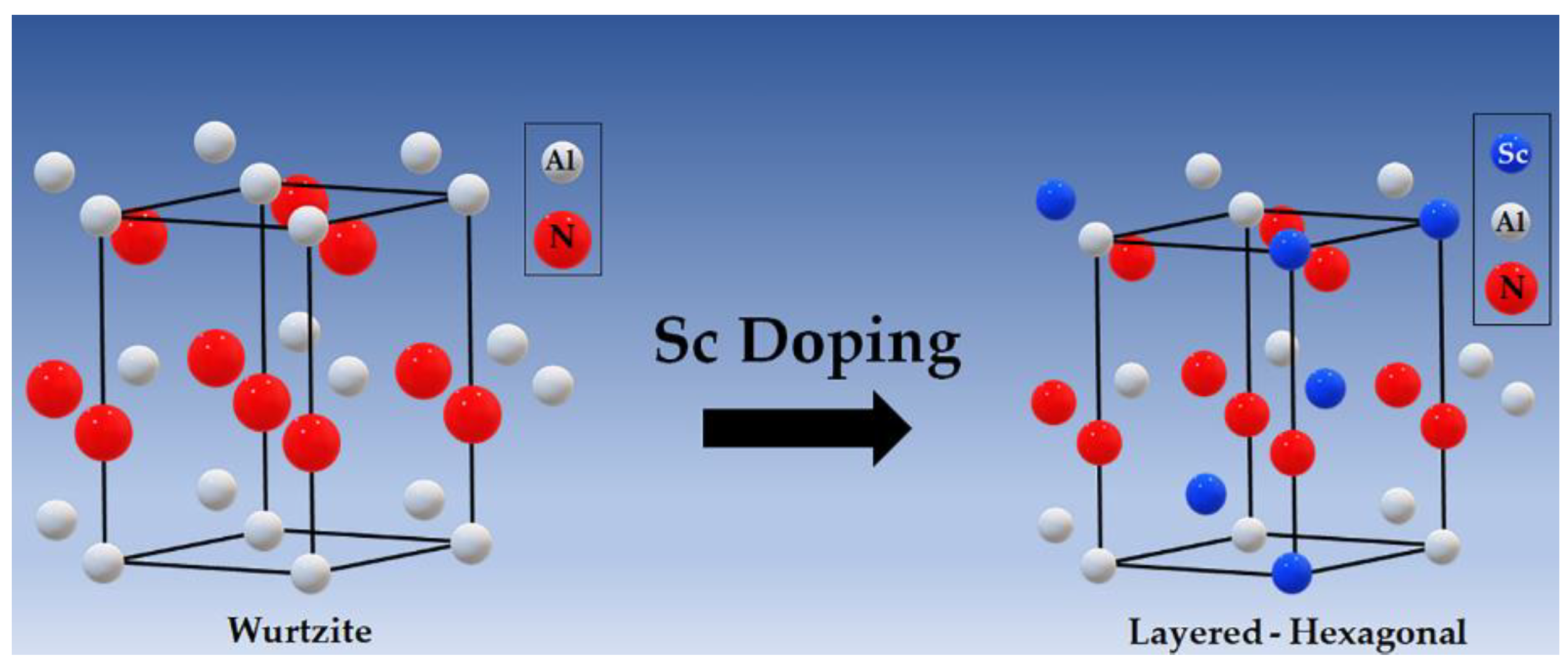
Figure 1. Crystal structure transition of AlN from wurtzite to layered-hexagonal with Sc doping to form ScxAl1−xN.
Coatings 13 00054 g001
Figure 2. Schematic representation of different target designs with (a) Sc-Al Alloy target, (b) pure Sc and pure Al targets for dual co-sputtering, and (c) ring-shaped segmented target with alternating Sc and Al tiles.
Coatings 13 00054 g002
Figure 3. Rocking curve FWHM of the (0002) reflections of ScAlN thin films under various working pressure conditions.
Coatings 13 00054 g003
Figure 4. Effect of sputtering atmosphere on (a) sputtering rate, (b) crystal quality, (c) resistivity, and (d) piezoelectric response. Reproduced with permission from Ref. [6].
Coatings 13 00054 g004
Figure 5. Effect of sputtering power on (a) XRD intensity, (b) FWHM, (c) RMS, and (d) piezoelectric response. Reproduced with permission from Ref. [26].
Coatings 13 00054 g005
Figure 6. Effect of substrate temperature on (a) XRD intensity, (b) FWHM, (c) grain size, and (d) piezoelectric response. Reproduced with permission from Ref. [27].
Coatings 13 00054 g006
Table 1. ScxAl1−xN properties.
PropertyReported Value[Ref]
Structural PropertiesDensity (g/cm3)3.255–3.456; ρ(x) = 3.806x + 3.255(1 − x) − 0.298x(1 − x)[15]
Elastic Modulus (GPa)535–269 (for x = 0–0.41)[16]
Elastic constant C11 (GPa)396.00–280.96; C11(x) = 285.12x + 396(1 − x) − 238.39x(1 − x) [15]
Elastic constant C12 (GPa)137.00–161.59; C12(x) = 180.57x + 137(1 − x) + 11.23x(1 − x)[15]
Elastic constant C13 (GPa)108.00–137.84; C13 = 141.70x + 108(1 − x) + 51.95x(1 − x)[15]
Poisson’s ratioν21 = 0.343 (when x = 0.5)[15]
Crystal structurewurtzite/layered-hexagonal[15]
Lattice constant (Ǻ)a = 3.0997; c = 4.59569[17]
Optical PropertiesEffective electron mass0.46 m0 (for x = 0.18)[18]
Refractive index (visible to IR)2.05[19]
Electrical PropertiesBreakdown field (MV/cm)12.44 (for x = 0.18)[18]
Mobility of electrons/holes (cm2/V-s)147–205 (for x = 0.18)[18]
Dielectric constant10.31–34.52; ε33 = 89.93x + 10.31(1 − x) − 62.48x(1 − x)[15]
Energy band gap (eV)4.29–6.15; Eg(x) = 6.15 − 9.32x (for x ≤ 0.2)[20]
Resistivity (1012 Ω-cm)1.0–3.5[10]
Thermal PropertiesThermal conductivity (W/m-K)3.0–8.0 (for x = 0–0.20)[21]
Coefficient of thermal expansion (×10−6/K)4.29–4.65 (for x = 0–0.41)[16]
Debye temperature (K)933 (for x = 0.18)/737 (for x = 0.25)[18,19]
Piezoelectric PropertiesPiezoelectric coeff. e15 (C/m2)−0.313–−0.135; e15 = 0.308x − 0.313(1 − x) − 0.528x(1 − x)[15]
Piezoelectric coeff. e31 (C/m2)−0.593–−0.829; e31 = −1.353x − 0.593(1 − x) + 0.576x(1 − x)[15]
Piezoelectric coeff. e33 (C/m2)1.471–3.642; e33 = 9.125x + 1.471(1 − x) − 6.625x(1 − x)[15]
Relative permittivity coeff. ε339.37–13.06 (for x = 0–0.26)[22]
Ferroelectric PropertiesFerroelectric switching (µC/cm2)~80–153[7,8,23]
Coercive field (MV/cm)2–5 (for x = 0.27–0.43)[7]
Table 2. Summary of sputtering deposited ScAlN growth conditions.
Author [Ref] (Year of Publication)SubstrateSputtering TypePower (W)/Power Density (W/cm2)Substrate Temperature (°C)Sputtering Pressure (Pa)Base Pressure (Pa)Gas Composition Ratio [N2:Ar] /%N2Target to Substrate Distance [mm]Final Composition (ScxAl1−xN)FWHM (°)Deposition Rate (nm/min)Film Thickness (um)Surface Roughness (nm)
Tominaga et al. [28] (2022)(100) SiRF magnetron sputtering200/3.983000.63.00 × 10−41:2/50%25x = 0.33.2–6.0NA4.0–4.5NA
Tominaga et al. [29] (2021)(100) SiRF magnetron sputtering200/3.983000.14, 0.25, 0.35, 0.45, 0.562.00 × 10−41:2/50%25NA2.3–4.7NA1–2NA
Rassay et al. [8] (2021)NADC magnetron sputtering2000, 3500, 5500/8.06, 4.80, 7.54280NANA15:6, 20:3, 28:1.6/NANAx = 0.22, 0.25, 0.302–2.8NA0.025–0.250NA
Liu et al. [25] (2021)Pt/(100) SiPulsed DC magnetron co-sputteringAl-target: 1000/12.34; Sc-target: 450/5.55350NANANANAx = 0.29NANA0.100NA
Liu et al. [9] (2021)Pt/(100) SiPulsed DC magnetron co-sputteringAl-target: 1000/12.34; Sc-target: 655/8.08350NANA20:80/20%NAx = 0.36NANA0.200NA
Zhang et al. [17] (2021)Mo/SiO2/AlN/SOIDC magnetron sputtering7500/10.283000.347NA1:3/25%70x = 0.294.13NA0.780NA
Wang et al. [30] (2020)Pt(111)/Ti/SiO2/siPulsed DC magnetron co-sputteringAl-target: 1000/12.34; Sc-target (x = 0.32): 555/6.85; Sc-target (x = 0.36): 655/8.08350NA8.30 × 10−220:80/20%33x = 0.32, 0.362.7–2.815.6–16.80.2NA
Dong et al. [31] (2019)PtDC magnetron sputtering140–190/NA240.3NA13:17/43.3%NAx = 0.1750.38–0.2923.30.7NA
Felmetsger et al. [24] (2019)(100) SiAC magnetron reactive Sputtering with segmented target2000–5000/NA24NANANANAx = 0.31.6NA0.500–2.002.3
Fichtner et al. [7] (2019)NADC reactive magnetron sputter deposition600/NA400NANA15:7.5/NANAx = 0.36NANA0.600NA
Tabaru et al. [32] (2019)(100) p-SiRF reactive magnetron sputtering400/8.782070.4, 1.05.00 × 10−54:6/NA70x = 0.44.6, 8.5NA2.3, 2.6NA
Henry et al. [33] (2018)(100) SiPulsed DC magnetron sputtering80, 90, 100, 110, 120/0.116, 0.127, 0.140, 0.156, 0.170350NANA1:3, 1:4, 1:5/25%, 20%, 16.7%NAx = 0.121.884NA0.750NA
Lozano et al. [34] (2018)(100) As-doped Si & (100) B-doped SiDC reactive balanced magnetron sputtering300, 500, 700/3.70, 6.17, 8.64240.53, 0.79, 1.061.00 × 10−21:3/25%45x = 0.262–524–901.00NA
Mertin et al. [35] (2018)NAPulsed DC magnetron sputtering/co-sputtering30.4 cm-Target: 7500/10.34; 10 cm-Target: 200–1000/2.55–12.74300–350NA1.00 × 10−51:2/33.3%NAx = 0, 0.1, 0.31, 0.421.2–2.012–60NANA
Perez-Campos et al. [36] (2017)(100) As-doped Si & (100) B-doped SiDC reactive balanced magnetron sputtering300, 500, 700, 900/3.70, 6.17, 8.64, 11.11240.26, 0.53, 0.79, 1.069.99 × 10−53:9/25%45x~0.23–0.262.5–1024–1101.00NA
Tang et al. [26] (2017)PT/Ti/SiRF reactive magnetron sputtering100, 120, 135, 145, 160/1.05, 1.26, 1.42, 1.52, 1.686000.471.50 × 10−43.4:7/32.7%120x = 0.152.38–6.55NA1.003.25–10.34
Felmetsger et al. [37] (2017)(100) SiAC powered S-gun sputtering2000/NA350NANA9:3.5/NANAx = 0.071.55NA1.003.3
Fichtner et al. [38] (2017)(100) c-SiPulsed DC reactive co-sputtering1000/NA3000.215.00 × 10−515:5.3/NANAx = 0.27, 0.291.7NA0.4–2NA
Li et al. [10] (2016)(100) p-Si & Ni-Cr-Mo (Hastelloy)DC reactive magnetron sputteringNA/1.16–2.106000.452.00 × 10−43.3:7NAx = 0.431.5–11NA1.1–2.02.0–4.9
Tang et al. [6] (2016)(100) p-SiDC reactive magnetron sputtering130/1.376000.4, 0.82.00 × 10−430:70, 35:65, 40:60, 50:50, 60:40/30%–60%100NA1.716.6–21.01.503–21
Zhang et al. [39] (2014)(0001) SapphireDC reactive magnetron sputtering130/1.376500.3–0.74.00 × 10−43.1:7–3.6:7/30.7%–34%NANA2.616.671.502.65
Akiyama et al. [40] (2013)(100) n-SiDual RF magnetron reactive co-sputteringNANANA1.20 × 10−6NANAx = 0.411.8–7.9NA0.500–1.10NA
Zukauskaite et al. [41] (2012)TiN(111)/Al2O3(0001)-100–200 nmMagnetically unbalanced reactive DC magnetron sputtering150/7.64400, 600, 8000.176.00 × 10−719.8:30/NANAx = 0, 0.1, 0.2, 0.31.0–2.0NA0.25NA
Akiyama et al. [29] (2010)(100) n-Si-600 umRF reactive magnetron sputtering300/6.582000.35.00 × 10−53:7/30%NAx = 0.382.3NA0.500–1.20NA
Hoglund et al. [42] (2010)ScN(111)/MgO(111)Magnetron sputter epitaxyAl-Target: 250, 230, 180, 130, 80; Sc-Target: 0, 20, 70, 120, 1708000.461.33 × 10−6NANAx = 0.4, 0.32, 0.26, 0.22NA4.20.080NA
Hoglund et al. [43] (2010)ScN(111)/MgO(111)Magnetron sputter epitaxyAl-Target: 0, 20, 60, 100, 140, 180, 200; Sc-Target: 200, 180, 140, 100, 60, 20, 06001.21.33 × 10−60.13:1.07/NANAx= 0, 0.1, 0.27, 0.49, 0.71, 0.86, 1NA5.40.05–0.06NA
Akiyama et al. [27] (2009)(100) n-SiDual RF magnetron reactive co-sputtering0–200/0–9.8727–5800.251.20 × 10−6NA/40%NAx = 0–0.432.3–7.5NA0.5–1.10.3–2.7
Akiyama et al. [5] (2009)(100) n-SiDual RF magnetron reactive co-sputtering0–200/0–9.875800.251.20 × 10−6NA/40%NAx = 0–0.431.8–7.9NA0.5–1.1NA
NA (Not Available) is used to indicate when specific parameters were not provided in the given literature.
Table 3. ScxAl1−xN films produced using various target designs.
ScxAl1−xN CompositionTarget CompositionRef
Single-Alloy-Target
x = 0.38Sc:Al = 42:58[45]
NASc:Al = 0.1:0.9[39]
x = 0.43Sc: Al = 0.1:0.9[10]
NASc:Al = 1:9[6]
x = 0.23–0.26Sc:Al = 0.4:0.6[36]
x = 0.15Sc:Al = 0.15:0.85[26]
x = 0.12Sc:Al = 12.5:87.5[33]
x = 0.26Sc:Al = 0.4:0.6[34]
x = 0.1, 0.31Sc:Al = 6:9.5, 15:28[35]
x = 0.3 Sc:Al = 8:92[24]
x = 0.36Sc:Al = 43:57[7]
x = 0.4Sc:Al = 43:57[32]
x = 0.29Sc:Al = 0.3:0.7[17]
Dual Co-Sputtering Target
x = 0, 0.1, 0.27, 0.49, 0.71, 0.86, 1Al (pure) and Sc (pure)[42]
x = 0.36Al (pure) and Sc (pure)[5]
NAAl (pure) and Sc (pure)[44]
x = 0.4, 0.32, 0.26, 0.22Al (pure) and Sc (pure)[43]
x = 0, 0.1, 0.2, 0.3Al (pure) and Sc (pure)[41]
x = 0.41Al (pure) and Sc (pure)[40]
x = 0.27, 0.29Al (pure) and Sc (pure)[38]
x = 0.42Al (pure) and Sc (pure)[35]
x = 0.175Al (pure) and Sc (pure)[31]
x = 0.32, 0.36Al (pure) and Sc (pure)[30]
x = 0.29Al (pure) and Sc (pure)[9]
x = 0.36Al(pure) and Sc (pure)[25]
x = 0.3Al(pure) and Sc (pure)[29]
x = 0.43Al(pure) and Sc (pure)[28]
Segmented Target
x = 0.3Segmented Al-Sc[24]
x = 0.22, 0.25, 0.30Segmented Al-Sc[8]
NA (Not Available) is used to indicate when specific parameters were not provided in the given literature.
Table 4. Comparison of various target designs.
Sc-Al Alloy TargetDual Co-Sputtering TargetSc-Al Segmented Target
  • Higher deposition rate
  • Applicable for industrial applications
  • Constant Sc content across large substrates
  • Easy Sc content tuning by adjusting target power
  • Reduced cost of target
  • Enables thickness reduction
  • Large tunability of Sc content
  • Large tailorability of residual film stress (independent of gas flows)
  • Expensive targets due to complicated metallurgy
  • Difficult tuning of Sc content
  • Residual stress tailoring only through altering reactive gas flow, which degrades film uniformity and crystallinity
  • Difficult to achieve tensile stress
  • Lower deposition rate
  • Less applicable for industrial applications
Disclaimer/Publisher’s Note: The statements, opinions and data contained in all publications are solely those of the individual author(s) and contributor(s) and not of MDPI and/or the editor(s). MDPI and/or the editor(s) disclaim responsibility for any injury to people or property resulting from any ideas, methods, instructions or products referred to in the content.