Article

Evaluating the Topological Surface Properties of Cu/Cr Thin Films Using 3D Atomic Force Microscopy Topographical Maps

by
Mohammad Sadeghi
1,
Amir Zelati
2,
Sahar Rezaee
3,*,
Carlos Luna
4,
Robert Saraiva Matos
5,
Marcelo Amanajás Pires
6,
Nilson S. Ferreira
7,
Henrique Duarte da Fonseca Filho
8,
Azin Ahmadpourian
3 and
Ştefan Ţălu
9,*
1
Mälardalens Högskola (EST), Mälardalen University, 722 20 Vasteras, Sweden
2
Department of Basic Sciences, Birjand University of Technology, Birjand 9719866981, Iran
3
Department of Physics, Kermanshah Branch, Islamic Azad University, Kermanshah 6718773654, Iran
4
Facultad de Ciencias Físico Matemáticas (FCFM), Universidad Autónoma de Nuevo León (UANL), Av. Universidad s/n, San Nicolás de los Garza 66455, Nuevo León, Mexico
5
Postgraduate Program in Materials Science and Engineering, Federal University of Sergipe, São Cristovão 49100-000, SE, Brazil
6
Department of Physics, Federal University of Ceará—UFC, Fortaleza 60180-020, CE, Brazil
7
Department of Physics, Federal University of Sergipe, São Cristovão 49100-000, SE, Brazil
8
Laboratory of Synthesis of Nanomaterials and Nanoscopy, Physics Department, Federal University of Amazonas-UFAM, Manaus 69067-005, AM, Brazil
9
The Directorate of Research, Development and Innovation Management (DMCDI), Technical University of Cluj-Napoca, 15 Constantin Daicoviciu St., 400020 Cluj-Napoca, Romania
*
Authors to whom correspondence should be addressed.
Coatings 2022, 12(9), 1364; https://doi.org/10.3390/coatings12091364
Submission received: 15 August 2022 / Revised: 6 September 2022 / Accepted: 15 September 2022 / Published: 19 September 2022
(This article belongs to the Section Corrosion, Wear and Erosion)

Abstract

:
In the present work, Cu/Cr thin films were deposited on substrates of a different nature (Si, Glass, Bk7, and ITO) through a thermal evaporation deposition method. Non-contact atomic force microscopy (AFM) was used to obtain 3D AFM topographical maps of the surface for the Cu/Cr samples. Various analyses were carried out to obtain crucial parameters for the characterization of the surface features. In particular, Minkowski functionals (including the normalized Minkowski volume, the Minkowski boundary, and the Minkowski connectivity) and studies of the spatial microtexture by fractal and multifractal analyses were carried out. Different roughness parameters (including arithmetical mean height, root mean square height, skewness, kurtosis, fractal dimension, Hurst coefficient, topographical entropy, and fractal lacunarity) were quantified in these analyses for the comparison of the surface morphology of the different samples. All the samples displayed non-Gaussian randomly rough surfaces, indicating the presence of multifractal features.

1. Introduction

The physical properties of thin films grown by deposition layers of different natures are directly related to their low dimensionality and multilayer structure. Over the past few decades, the scientific community has devoted considerable efforts to exploring and understanding the new physical phenomena arising from surface effects and interfacial interactions in these materials [1,2,3,4,5]. One crucial challenge for surface engineering is finely controlling the nanocrystalline thin film grain size and boundary to modulate the properties for different technological requirements. In this regard, Cu thin films with high strength and electrical and thermal conductivity are crucial for the design of micro-electro-mechanical systems (MEMS) and electronic nanodevices [6,7,8]. However, these films’ tensile ductility and thermal stability strongly depend on the grain boundaries’ volume fraction, which can be tuned with dopant atoms (such as Cr and Pt) and alloying [9,10]. The Cu/Cr systems usually present small solubilities (less than 0.1 at.% below 1000 °C) [11], and therefore, magnetron sputtering deposition is a versatile technique for the non-equilibrium preparation of alloyed thin films from an immiscible element. Recently, some researchers have reported the deposition of Cu/Cr thin films with interesting interfacial phenomena, such as the Cu grain growth within Cr grain boundaries and vice versa [9] and the formation of nanotwins [10]. These microstructural properties are associated with the mechanical behavior of the film and allow tuning control of its hardness [9,10]. Furthermore, in the study of both surface and interfacial effects, the roughness of the layers plays an essential role, which strongly depends on the deposition parameters, including the nature of the substrate and the deposited layers, the working pressure, the temperature, the deposition rate, and the deposition time, among others [12,13,14,15,16,17,18]. For this reason, it is essential to have accurate characterization techniques and advanced methodologies and tools for analyzing the produced experimental data of the 3D surface morphology of thin films.
Atomic force microscopy (AFM) is a powerful characterization technique to obtain three-dimensional (3D) atomic force microscope (AFM) topographical maps of surfaces [19,20]. Additionally, a variety of methods have emerged and consolidated during the last decade for the analysis of the three-dimensional (3D) atomic force microscope (AFM) maps to differentiate and quantify characteristic parameters in the determination of the complexity of the layer surface roughness [21,22,23,24,25,26,27,28,29]. Such methods include the determination of Minkowski functionals [21,22,23], fractal [24,25,26], and multifractal [27,28,29] analyses, among others. The combination of these methods in the analysis of AFM images is necessary to have a deeper understanding of the dependence of the grain size and film roughness on the experimental deposition parameters and to clarify the interfacial and surface phenomena that govern the physical properties of these low dimensional systems, generating new scientific knowledge with potential technological applications.
In the present work, Cu/Cr thin films constituted by a Cr layer with a thickness of 25 nm deposited onto different kinds of substrates (Si, Glass, Bk7, and ITO) at a temperature of 150 °C, and a Cu layer with a thickness of 250 nm deposited on the chromium thin film, were prepared using the thermal evaporation deposition method. The microstructure surface of these films was studied using non-contact atomic force microscopy, and the obtained data were analyzed by applying different methods to characterize the complexity of the surface topography with the quantification of roughness parameters for the comparison of the studied samples.

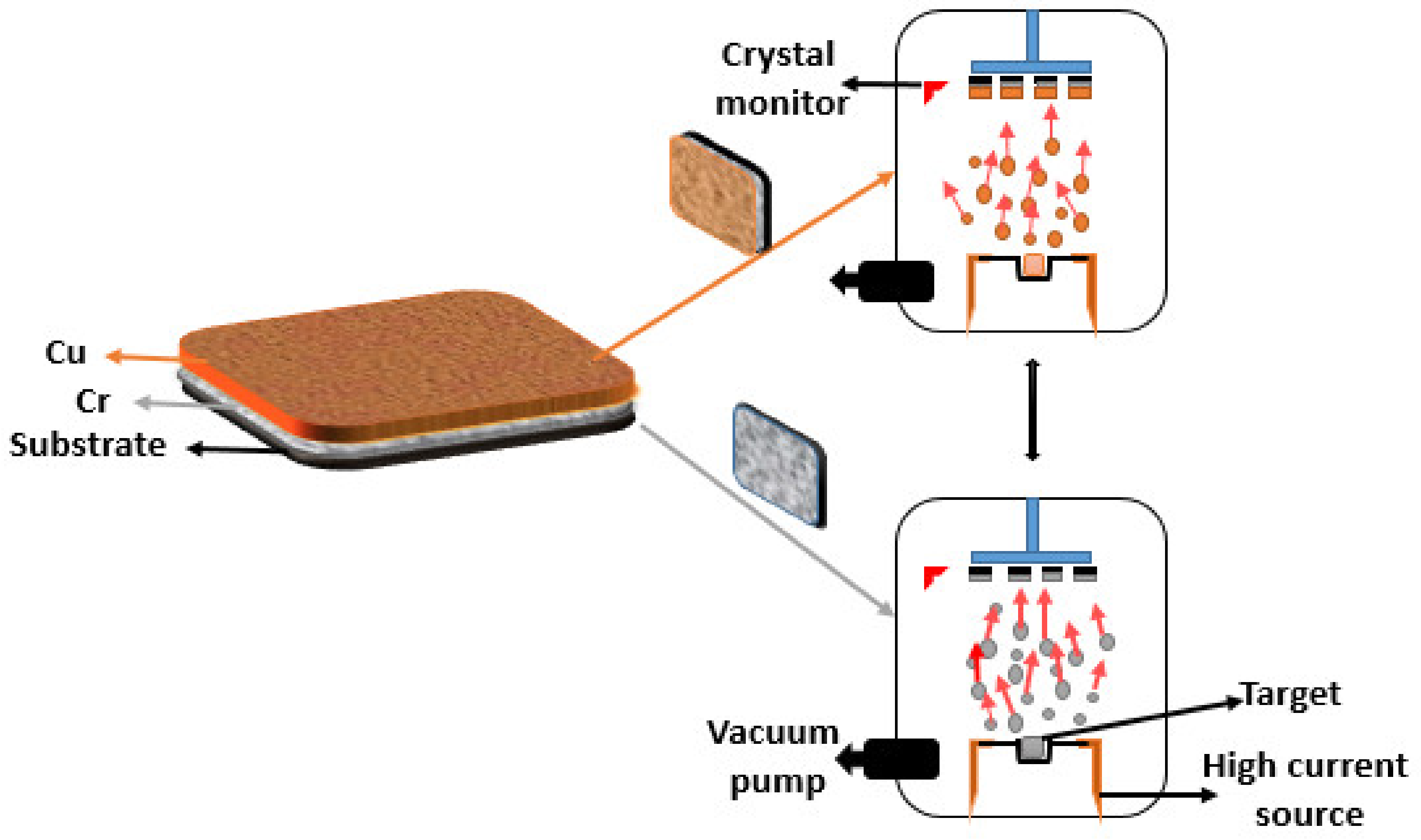
2. Materials and Methods

Herein, we use the thermal evaporation method to prepare the Cu/Cr multiplier. First, a chromium thin film with a thickness of 25 nm is grown on Si, Glass, Bk7, and ITO substrates at a temperature of 150 °C. Then, a copper thin film with a thickness of 250 nm is deposited on the chromium thin film deposited on the substrates at a temperature of 70 °C. In this study, the process of deposition using the thermal evaporation deposition method is such that the required working pressure is supplied by two rotary and diffusion pumps. Then, the substrates are heated to the required temperature by the heater. Afterward, the required electric current through the tungsten plant containing the target material (chromium or copper with a purity of 99.99%) induces the evaporation of material molecules to move down to the substrate due to the pressure difference between the plant, resulting in the formation of a thin film of chromium or copper on the substrate. Thus, all deposition parameters are kept constant, and the only difference is used during the Cu/Cr film production. The employed parameters to prepare the films are given in Table 1.
It should be mentioned that the deposition process is performed again to ensure reproducibility. An overview of the deposition conditions is given in Figure 1.
The thickness of the films is controlled using the Sigma Thickness Measurement Instruments, SQM-160 (Sigma Instruments, Cranberry Twp., PA, USA) Thin Film Deposition Monitor, which uses a quartz crystal sensor to measure the deposition rate and thickness of thin films to be deposited on a substrate (more details are described in Table 1). EDS analysis is performed by the Oxford Instruments (Abingdon, UK) EDS Microanalysis X-MAX-80 model, being used to identify the percentage of the elements in the formed films on the glass and silicon substrates. Moreover, a detailed study of the surface morphology of the films is performed. Four images of each sample are obtained with 3 × 3 µm2, (256 × 256) pixels, and all measurements are obtained at room temperature in air and 45% ± 1% relative humidity.

3. Results and Discussion
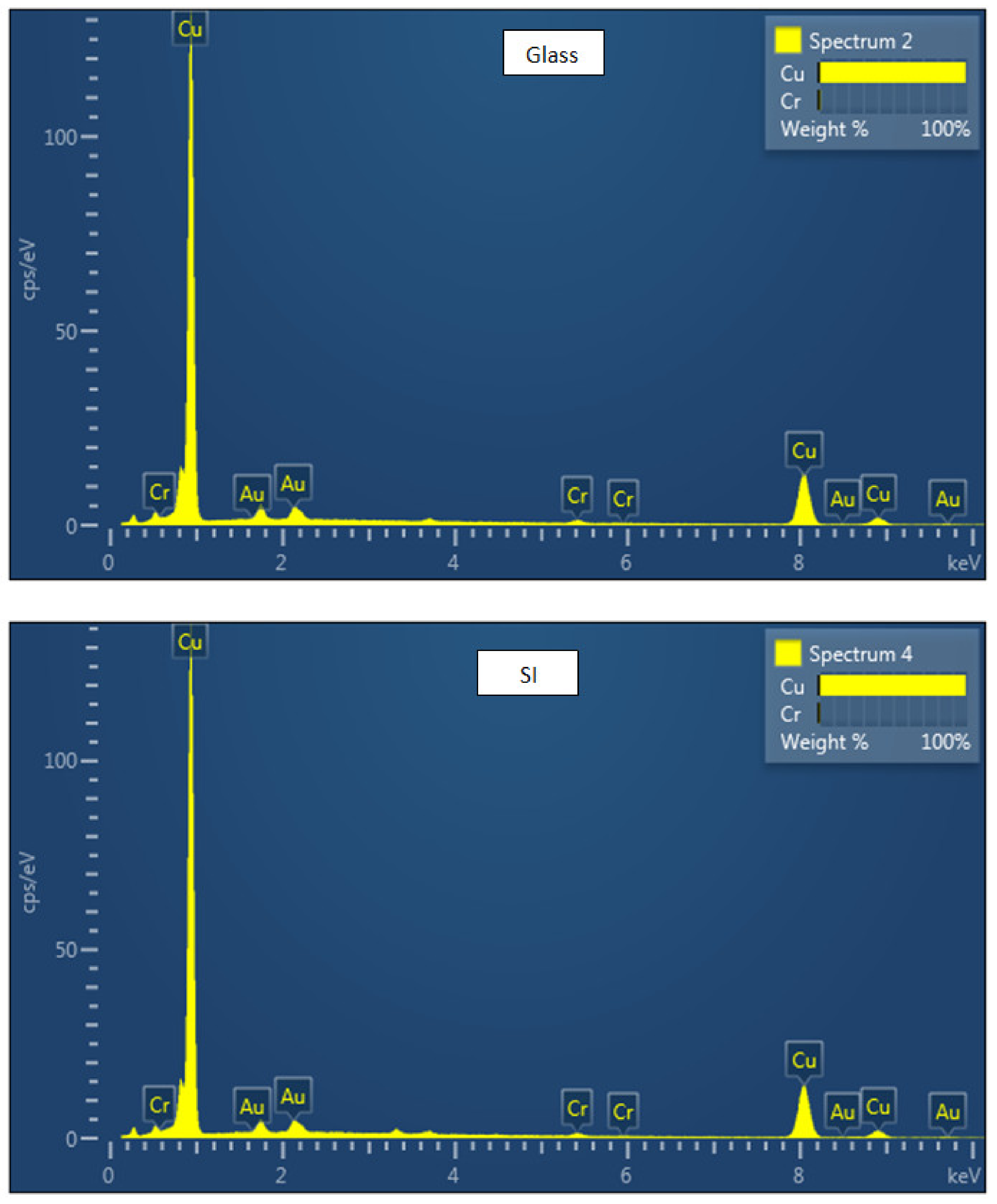
3.1. EDS Analysis

Figure 2 and Table 2 present the validations of Cr and Cu with a concrete stoichiometry exposed from EDS with ≈100 at.%. The EDS spectra can prove the formation of the Cr and Cu films on the substrates.

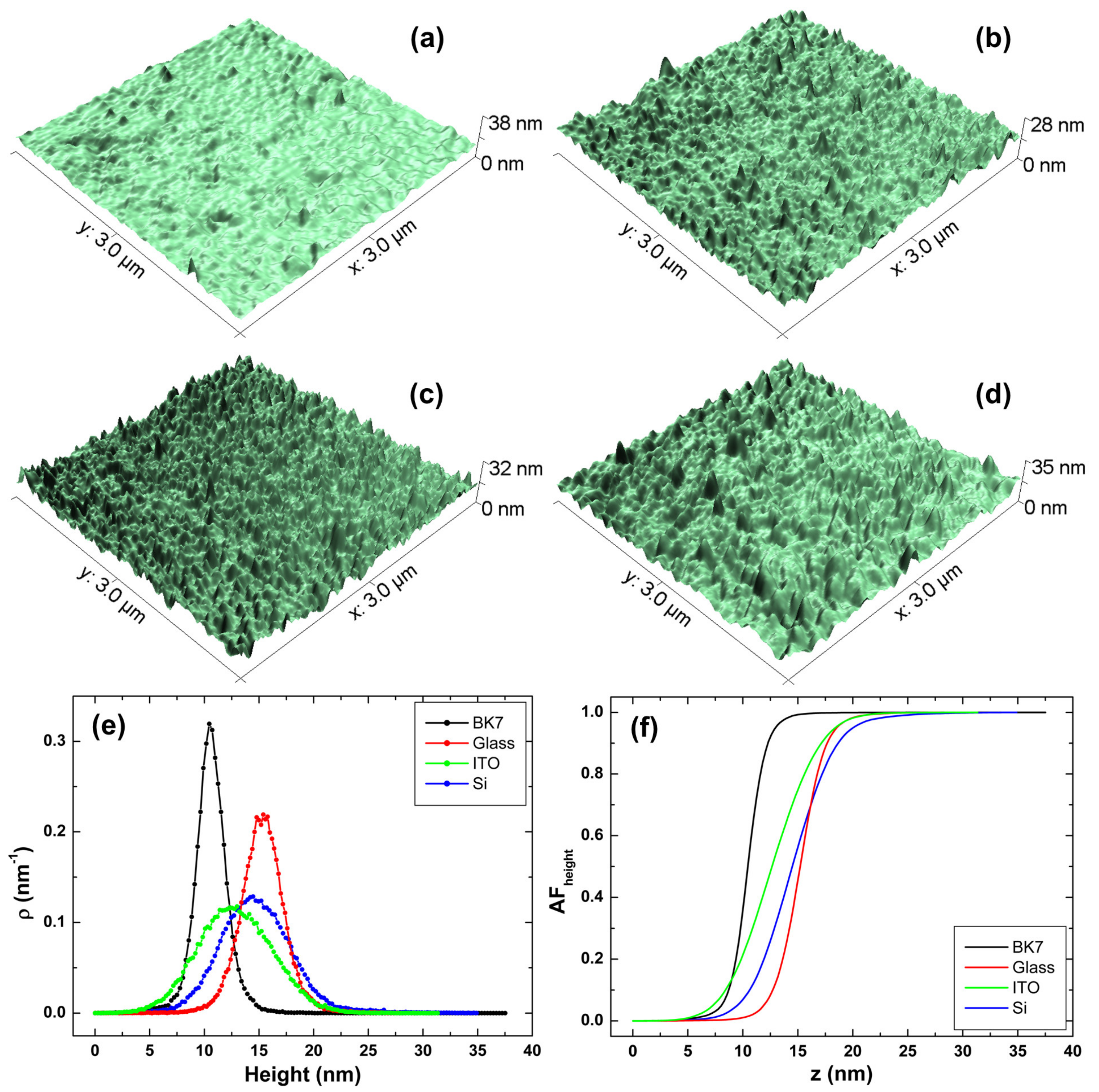
3.2. Height-Based Analysis

Three-dimensional AFM topographical maps are helpful for identifying specific spatial patterns in thin films [30,31,32]. It is worth remembering that the possible errors in the detection processes and also in the noise reduction of the surface topography measurement are extremely important. In addition, current processing software has filters and routines that are very useful for reducing the noise produced during measurement. AFM systems have anti-vibration tables and specific chambers to avoid the influence of mechanical vibrations that would create erroneous artifacts in the image. Thus, to avoid such problems, as already mentioned, the AFM measurements were performed in non-contact mode, indicating that the interaction between tip and surface was caused by long-range forces acting in a regime of attractive forces. This mode can bring artifacts to the image in the case of large scans, which is not the case in the work presented here [33,34]. The images obtained in this work were processed using the MountainsMap software to evaluate the height-based morphological parameters according to the ISO 25178-2: 2012 standard [35]. In Figure 3a–d, it is clear the existence of a hierarchical structure where the roughness is branched over multiple scales. Notably, the conformation of Cu/Cr layer-by-layer on the BK7 substrate promoted the formation of a smoother morphology compared to the surfaces generated on glass, ITO, and Si substrates. Previously, Mwema et al. [36] deposited pure Al thin films on different substrates and showed that the substrate type plays an important role in informing unique nanoscale surface aspects. In this regard, it is also possible to conclude that the morphologies generated over BK7, glass, ITO, and Si substrates have unique surface aspects, explicitly, different rough peaks arrangement and rough profiles. In this regard, the substrates’ different rough profiles and morphologies are behind their different observed morphologies.
Furthermore, it is worth mentioning that although BK7 and glass are materials classified as glasses, their manufacturing process leads to the formation of surfaces with different morphologies and roughness. Herein, we found rough surfaces of 6.77 ± 1.36 nm and 6.82 ± 2.87 nm for the BK7 and glass, respectively (Table S1). These values are significantly higher than previously reported values of 0.40 nm (BK7) [37] and 0.5 nm (glass) [38]. Moreover, the distributions of particles on the surface of BK7 and glass exhibit different patterns, showing that these substrates have different surface microtextures, as seen in Figure S1a,b. However, ITO and Si substrates display different morphologies and smoother surfaces with a roughness of 1.89 ± 0.05 nm and 0.85 ± 0.45 nm, respectively (Figure S1c,d). Then, subtracting statistically similar surface roughness induced the growth of smoother surfaces, with a slightly different roughness of 1.62 ± 0.28 nm and 1.90 ± 0.22 nm for the Cr/Cu films deposited on the BK7 and Glass (Table 3). Nevertheless, ITO and Si substrates, which have a smoother surface compared to BK7 and glass, induced the growth of Cr/Cu films with similar roughness of 3.20 ± 0.22 and 3.32 ± 0.42 nm (Table 3). This proves that the roughness and morphology of the substrates are key factors that influence the formation of the surface of Cr/Cu films deposited by the thermal evaporation method.
Furthermore, the thermal behavior of the substrate at 150 °C can also play an important role in forming different morphologies and roughness of the films. It is known that at 150 °C, BK7 exhibits a coefficient of thermal expansion of ~7.6 × 10⁻⁶ °C−1 [39], while the value reported for single glass is ~6.45 × 10⁻⁶ °C−1 [40]. Likewise, ITO and Si have different coefficients of thermal expansion, explicitly, ~5.81 × 10⁻⁶ °C−1 [41] and ~3.5 × 10⁻⁶ °C−1 [42], respectively. The roughness values are reported to be 1.62 (BK7), 1.90 (glass), 3.20 (ITO), and 3.32 nm (Si) (Table 2), confirming that the different thermal behaviors of the substrates are also responsible for the formation of different morphologies and roughness. This occurs because at 150 °C, the diffusion of heat along the surfaces occurs differently, which allows the formation of different molds of the Cr film on the substrates due to the different arrangement of the atoms on the surface. Further, the Cu films are formed into the rough profile generated by displaying different morphologies and roughness patterns.
In Figure 3e, the height histogram reveals that the roughness of the films is well-spread around a mean value, indicating that the process of formation of the surface was well controlled. Moreover, the quality of the surfaces is again stressed by the Abbott–Firestone (AF) curves, where in Figure 3f, we notice a robust presence of the typical S-shape for all the samples. The Cu/Cr surface height-based morphological parameters are summarized in Table 3. As can be seen, the main roughness parameters Sa (arithmetical mean height) and Sq (root mean square height) are dependent on the substrate type. This indicates that different substrates form Cu/Cr surfaces with unique 3D spatial patterns. As a result of its smoother morphology (Figure 3a), the surface formed over the BK7 substrate exhibits a less rough topographic profile. Additionally, regarding the height distribution shape, we can note that the curves shown in Figure 3e suggest that the height histograms follow a Gaussian distribution. However, the values of skewness (Ssk) and kurtosis (Sku) presented in Table 3 show that this hypothesis is invalid. In fact, it was not observed the combination of Ssk ~0 and Sku ~3 [43], signals that the samples have non-Gaussian distributions. This means that all samples have surfaces with long-range spatial correlations, confirming the visual analysis from Figure 3a–d. Qualitatively, the Cu/Cr layer-by-layer surfaces formed over BK7 and glass are spiky (Sku > 3) [43,44], while those generated on ITO and Si are bumpy (Sku < 3) [45].

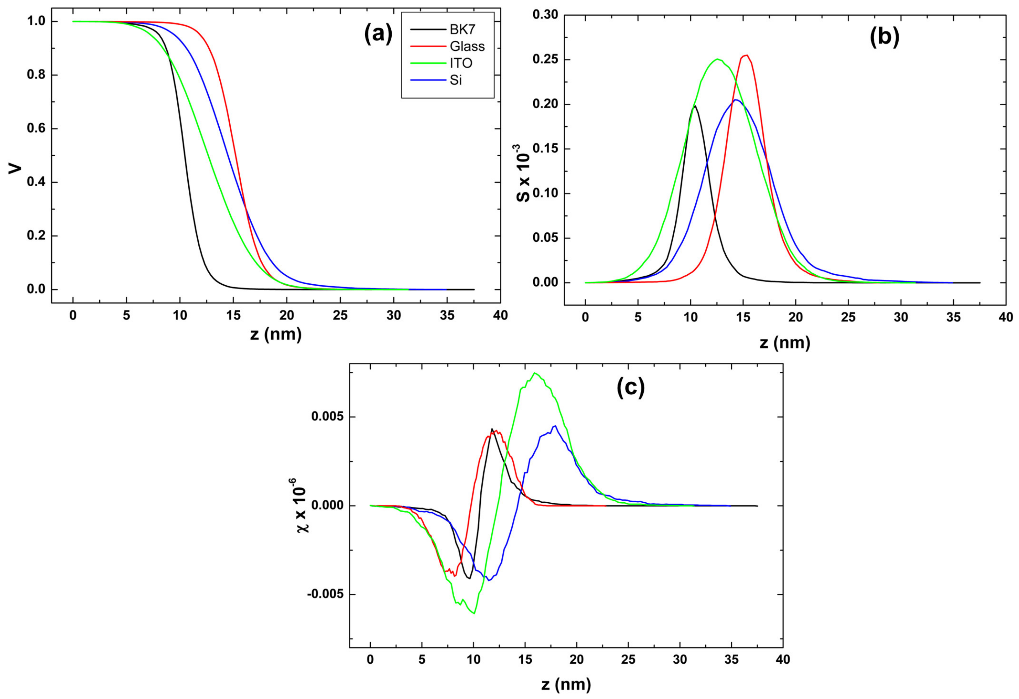
3.3. Minkowski Functionals

The Minkowski functionals (MFs)of the samples, which are geometrical, mathematical approaches widely used to study irregular morphologies [46], are represented by the curves exposed in Figure 4a–c. As can be seen, all curves exhibit the typical patterns observed for randomly rough surfaces [47]. The normalized Minkowski volume (V) presents a sharp decline between 10 nm < z < 25 nm, which agrees with the fast increase in the Abbott–Firestone curve in Figure 3f around the same spatial region. In turn, the Minkowski boundary (S) agrees with the height histogram in Figure 3e. Thus, it is evident that the largest increase in the V curve occurs at the thresholds close to the S curve’s mean value, pointing out that a large part of the material is around the mean surface. Such patterns again stress a high quality in the surface’s formation process. In addition, Figure 4c shows that the Minkowski connectivity χ presents the deepest minimum value for the sample deposited on the ITO substrate, indicating that isolated holes, compared to the others, more predominantly characterize such material. This signals that the ITO substrate forms a surface that potentially has interesting features in the context of percolation.

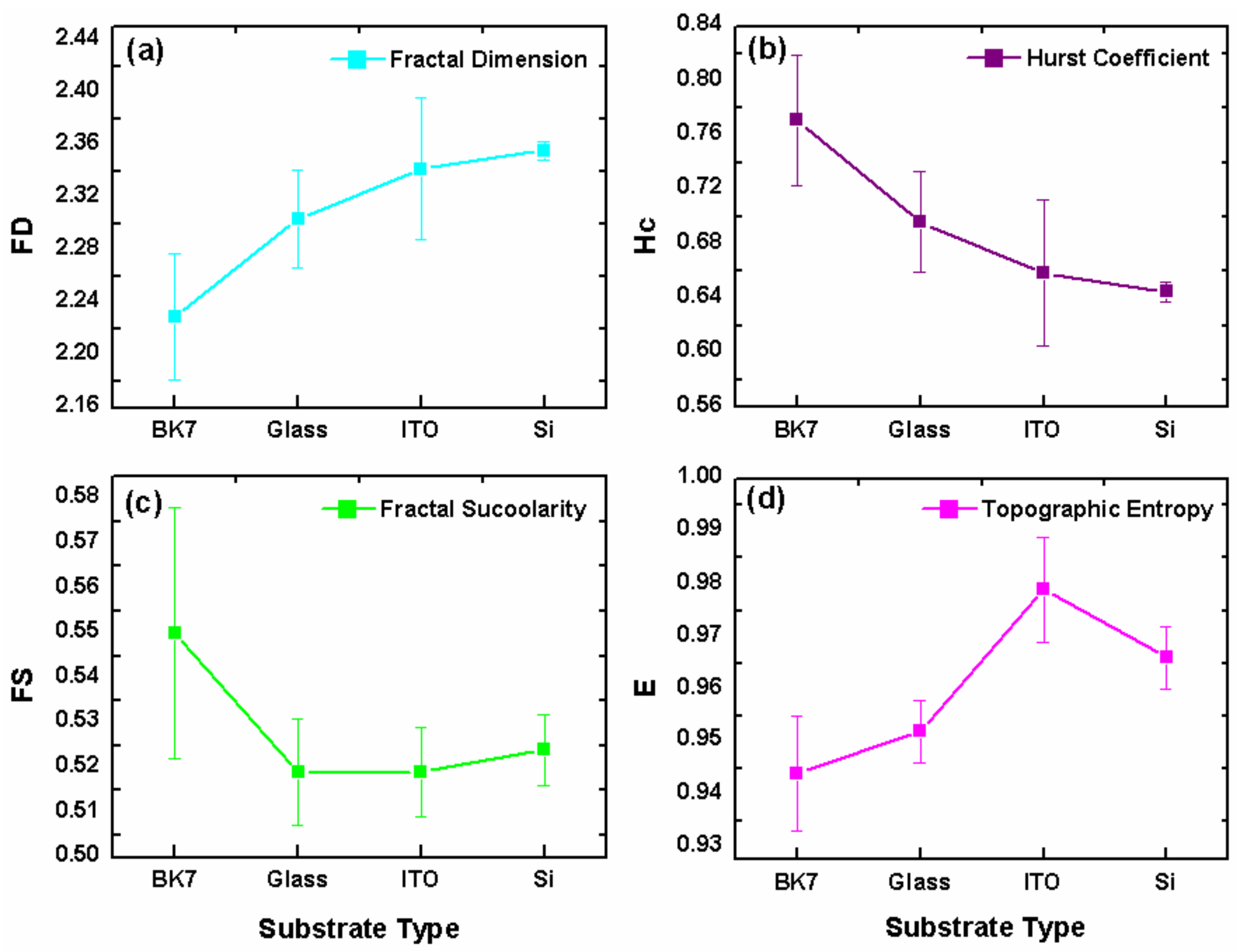
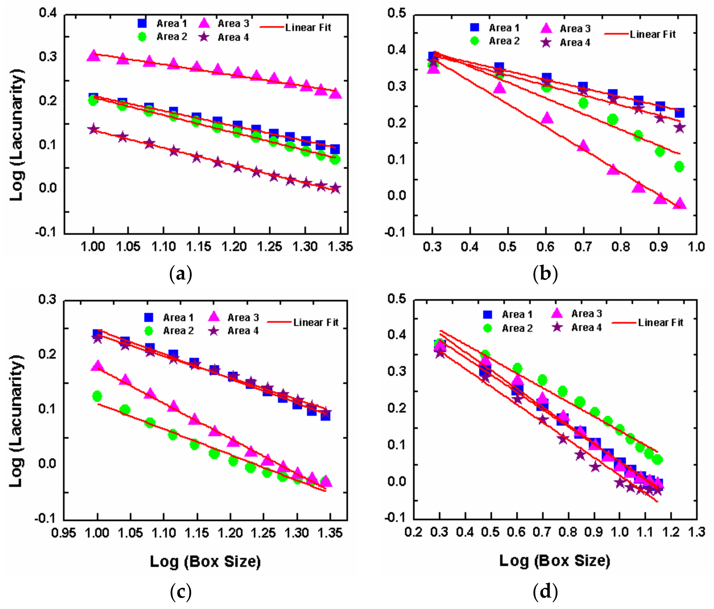
3.4. Analysis of the Films’ Spatial Microtexture

In Figure 5a–c, we see measures related to the fractality of the film’s surface, which are important parameters used to identify different spatial configurations of the surface microtexture [48,49]. In this way, Figure 5a–b displays the behavior of the fractal dimension (FD) and Hurst coefficient (Hc), whose average values were computed to be 2.229 and 0.771 (BK7), 2.304 and 0.696 (Glass), 2.342 and 0.659 (ITO), and 2.356 and 0.645 (Si), respectively. These results show that the Si substrate promotes the formation of Cu/Cr surfaces with the largest FD and smallest Hc, signaling that the Si surfaces have a high spatial complexity compared with the other samples. Such an aspect is associated with their high roughness value recorded.
On the other hand, the fractal succolarity (FS) average values are 0.550 (BK7), 0.519 (glass), 0.519 (ITO), and 0.524 (Si), and their dependence on the substrate used is shown in Figure 5c. Our observation shows that for BK7, we have the largest fractal succolarity, indicating that such a surface has a high percolation degree, suggesting that this surface can be more easily lubricated than others. Finally, the average values for the topographical entropy based on information theory (E) were found to be 0.994 (BK7), 0.952 (glass), 0.979 (ITO), and 0.966 (Si). The trend of this parameter is displayed in (Figure 5d). It reveals that although all topographies have a high degree of uniformity [50], as their normalized topographic entropies reached a high value (>0.95), the samples deposited on the ITO and Si substrates have significantly higher values. In other words, this means that these samples have the distribution of topographical heights evenly distributed along the surface, which is a remarkable characteristic of these samples. Some previous reports have associated the topographical uniformity of the rough profile with some physical properties, e.g., friction, wear, and adhesion [51,52,53]. A higher topographical entropy value suggests that the possibility of material failure is minimized. Thus, the ITO and Si samples perform best as a more uniform surface material.
Another important aspect of the surface microtexture is its homogeneity, which was evaluated by fractal lacunarity. The linear pattern in the log-log plot depicted in Figure 6 reveals that the lacunarity behaves as a spatial power law. This indicates the functional relationship in which the stochastic deposition of layer-by-layer Cu/Cr thin films on BK7, Si, and glass substrates did not favor the formation of purely random interfaces. However, it favored the emergence of surfaces with a combination of long-range correlation and a lacunar distribution across multiple scales.
Such a feature is in congruence with the non-Gaussian height distribution discussed previously. Furthermore, the lacunarity coefficients (σ) were found to be 0.329 (BK7), 0.487 (glass), 0.391 (ITO), and 0.451 (Si). A lower value of σ means that the surface microtexture is more homogeneous [53,54]. This indicates that the films deposited on the BK7 substrate have a more homogeneous surface microtexture than the other substrates. Despite that, the ITO sample also has a low value compared to the glass and Si samples. Combining this information with the topographical entropy analysis, it is possible to conclude that the ITO sample has the most uniform and homogeneous surface microtexture, which makes it a promising material for technological applications.

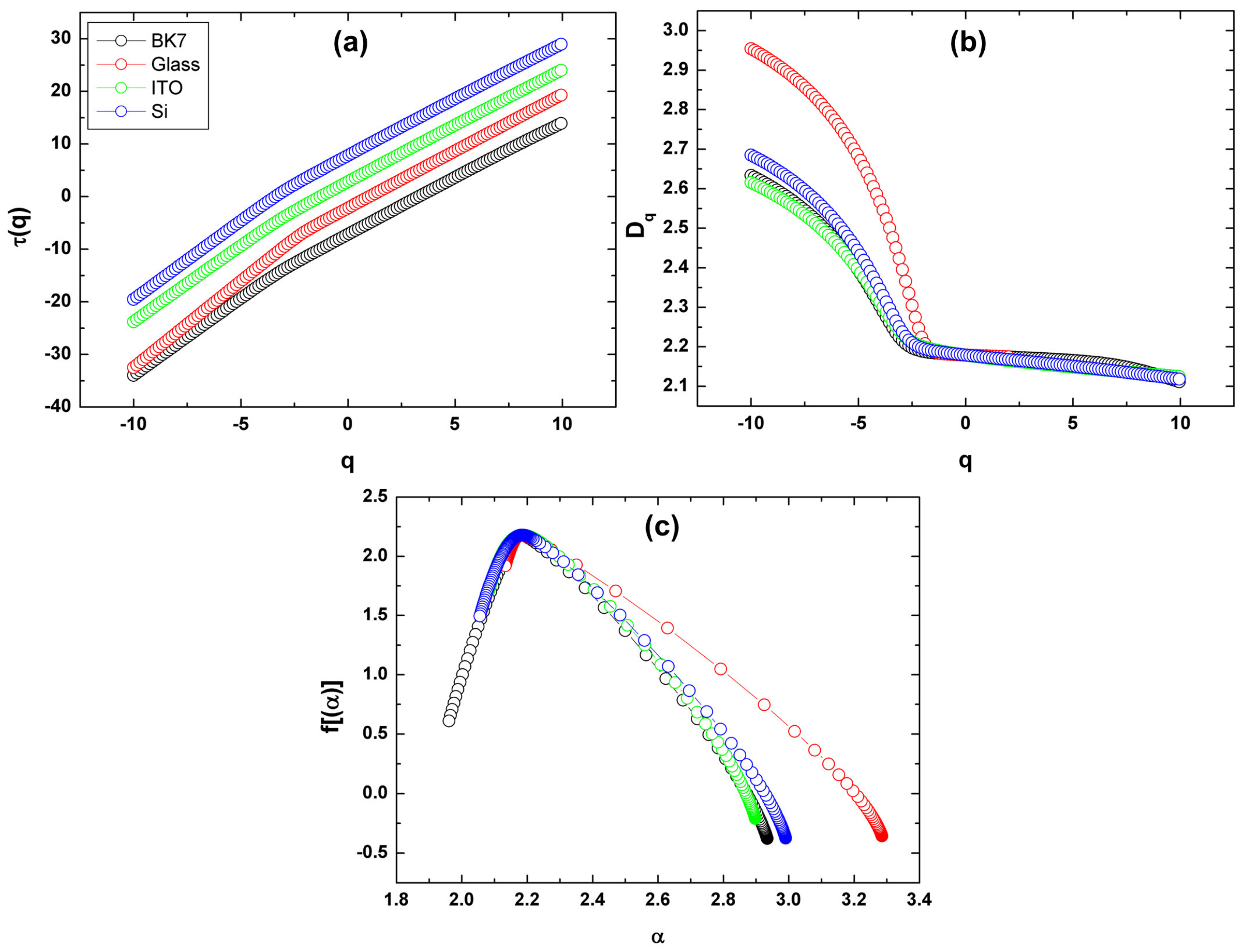
3.5. Multifractal Analysis

The multifractal analysis can provide a more comprehensive description of fractal surfaces [55,56]. In Figure 7a, we see that all samples display multifractality since the mass exponent τ(q) versus q deviated from a single linear trend. Such multifractality is endorsed by the non-constant behavior of Dq versus q, shown in Figure 7b as well as by the typical concave curve of the multifractal spectrum f(α) versus α, shown in Figure 7c, confirming the multifractal behavior for all our samples in agreement with the long-range correlation previously discussed. Apart from this, it is evident that Figure 7b–c reveals that the glass samples exhibit distinguished features, as documented in Table 4, which provides a collection of measures related to the multifractal spectra. The largest width of the spectrum Δα (the difference between αmax and αmin) occurs for the glass sample, which means that their topographies have the highest degree of multifractality. The layer-by-layer deposition of Cu/Cr on Glass occurred with a preferential growth of a hierarchical distribution of roughness that branches across several spatial scales with a wide range of fractal dimensions. This multiscale self-affine growth was also present for the other substrates (Si, BK7, and ITO), but with much weaker intensity due to the inferior degree of multifractality, as shown in Figure 7 and Table 4.
The width of the multifractal spectrum (Δα) and the spectrum arms’ heights difference (Δf) are computed using the following expressions [55,56,57]:
Δα = αmax − αmin
Δf = f(αmin) − f(αmax)

4. Conclusions

We successfully prepared Cu/Cr thin films constituted by a Cr layer with a thickness of 25 nm deposited onto different kinds of substrates at a temperature of 150 °C, and a Cu layer with a thickness of 250 nm deposited on the chromium thin film, using the thermal evaporation deposition method. Important differences and common properties of the surface features of Cu/Cr thin films grown in different substrates (Si, glass, Bk7, and ITO) were identified.
All samples exhibited non-Gaussian surfaces with a multifractal nature. The sample grown on the Si substrate exhibited a rough surface with more complexity than the others, as reflected in its high value of fractal dimension and the smallest Hurst coefficient.
The sample deposited on the ITO substrate presented a low fractal succolarity with more isolated holes and a high topographic entropy value (>0.95), which are interesting properties from a technological point of view due to their association with percolation, friction, wear, and adhesion.
The Cu/Cr surfaces deposited over BK7 and glass substrates were spiky (Sku > 3), while those grown on ITO and Si substrates were bumpy (Sku < 3). The samples grown on the BK7 substrate had the largest fractal succolarity and the smallest fractal lacunarity.

Supplementary Materials

The following supporting information can be downloaded at: https://www.mdpi.com/article/10.3390/coatings12091364/s1, Figure S1: 3D AFM topographical maps of (a) BK7, (b) Glass, (c) ITO, and (d) Si substrates; Table S1: Roughness of BK7, Si, and Glass substrates, according to ISO 25178-2:2012. The average results were expressed as mean values and standard deviation.

Author Contributions

M.S.: Conceptualization, Writing; A.Z.: Methodology, Writing, Investigation; S.R.: Formal analysis, Investigation, Supervision; C.L.: Reviewing and Editing, Investigation; R.S.M.: Resources, Software, Investigation; M.A.P.: Resources, Editing; N.S.F.: Investigation, Software; H.D.d.F.F.: Software, Formal analysis, Writing; A.A.: Investigation, Reviewing and Editing; Ş.Ţ.: Reviewing and Editing, Funding acquisition, Project administration. All authors have read and agreed to the published version of the manuscript.

Funding

This research received no external funding.

Institutional Review Board Statement

Not applicable.

Informed Consent Statement

Not applicable.

Data Availability Statement

Data sharing is not applicable to this article.

Conflicts of Interest

The authors declare no conflict of interest.

References

  1. Tagantsev, A.K.; Gerra, G. Interface-induced phenomena in polarization response of ferroelectric thin films. J. Appl. Phys. 2006, 100, 051607. [Google Scholar] [CrossRef]
  2. Korotcenkov, G. Metal Oxide-Based Thin Film Structures: Formation, Characterization and Application of Interface-Based Phenomena; Pryds, N., Esposito, V., Eds.; Elsevier: Amsterdam, The Netherlands, 2018; ISBN 978-0-12-811166-6. [Google Scholar]
  3. Lee, H.Y.; Al Ezzi, M.M.; Raghuvanshi, N.; Chung, J.Y.; Watanabe, K.; Taniguchi, T.; Garaj, S.; Adam, S.; Gradecak, S. Tunable Optical Properties of Thin Films Controlled by the Interface Twist Angle. Nano Lett. 2021, 21, 2832–2839. [Google Scholar] [CrossRef] [PubMed]
  4. Agrawal, P.; Büttner, F.; Lemesh, I.; Schlotter, S.; Beach, G.S. Measurement of interfacial Dzyaloshinskii-Moriya interaction from static domain imaging. Phys. Rev. B 2019, 100, 104430. [Google Scholar] [CrossRef]
  5. Xiong, S.; Yin, S.; Wang, Y.; Kong, Z.; Lan, J.; Zhang, R.; Gong, M.; Wu, B.; Wang, X. Organic/inorganic electrochromic nanocomposites with various interfacial interactions: A review. Mater. Sci. Eng. B 2017, 221, 41–53. [Google Scholar] [CrossRef]
  6. Anderoglu, O.; Misra, A.; Wang, H.; Ronning, F.; Hundley, M.F.; Zhang, X. Epitaxial nanotwinned Cu films with high strength and high conductivity. Appl. Phys. Lett. 2008, 93, 083108. [Google Scholar] [CrossRef]
  7. Mehmood, B.; Khan, M.I.; Iqbal, M.; Mahmood, A.; Al-Masry, W. Structural and optical properties of Ti and Cu codoped ZnO thin films for photovoltaic applications of dye sensitized solar cells. Int. J. Energy Res. 2021, 45, 2445–2459. [Google Scholar] [CrossRef]
  8. Roa, S.; Sirena, M. Size effects on the optimization of the mechanical resistance and the electrical conductivity of Cu thin films. Mater. Today Commun. 2021, 28, 102572. [Google Scholar] [CrossRef]
  9. Chang, C.A. Reduced Cu-Cr mixing and reduced Pt-Cu interdiffusion by oxygen in Cu/Cr and Pt/Cu/Cr thin films. J. Appl. Phys. 1982, 53, 7092–7094. [Google Scholar] [CrossRef]
  10. Li, X.G.; Cao, L.F.; Zhang, J.Y.; Li, J.; Zhao, J.T.; Feng, X.B.; Wang, Y.Q.; Wu, K.; Zhang, P.; Liu, G.; et al. Tuning the microstructure and mechanical properties of magnetron sputtered Cu-Cr thin films: The optimal Cr addition. Acta Mater. 2018, 151, 87–99. [Google Scholar] [CrossRef]
  11. Hansen, M.; Anderko, K.; Salzberg, H.W. Constitution of binary alloys. J. Electrochem. Soc. 1958, 105, 260C. [Google Scholar] [CrossRef]
  12. Merche, D.; Vandencasteele, N.; Reniers, F. Atmospheric plasmas for thin film deposition: A critical review. Thin Solid Film. 2012, 520, 4219–4236. [Google Scholar] [CrossRef]
  13. Ahmadpourian, A.; Luna, C.; Boochani, A.; Arman, A.; Achour, A.; Rezaee, S.; Naderi, S. The effects of deposition time on surface morphology, structural, electrical and optical properties of sputtered Ag-Cu thin films. Eur. Phys. J. Plus 2016, 131, 1–7. [Google Scholar] [CrossRef]
  14. Ghobadi, N.; Ganji, M.; Luna, C.; Arman, A.; Ahmadpourian, A. Effects of substrate temperature on the properties of sputtered TiN thin films. J. Mater. Sci. Mater. Electron. 2016, 27, 2800–2808. [Google Scholar] [CrossRef]
  15. Vahl, A.; Veziroglu, S.; Henkel, B.; Strunskus, T.; Polonskyi, O.; Aktas, O.C.; Faupel, F. Pathways to tailor photocatalytic performance of TiO2 thin films deposited by reactive magnetron sputtering. Materials 2019, 12, 2840. [Google Scholar] [CrossRef]
  16. Salunkhe, P.; AV, M.A.; Kekuda, D. Investigation on tailoring physical properties of Nickel Oxide thin films grown by dc magnetron sputtering. Mater. Res. Express 2020, 7, 016427. [Google Scholar] [CrossRef]
  17. Zhang, Q.; Zhang, Z.; Liu, Y.; Wang, Z. Crystallization and Composition of Ni-C/Ti Multilayer with Varied Ni-C Thickness. Coatings 2022, 12, 1144. [Google Scholar] [CrossRef]
  18. Kim, H.K.; Kim, S.M.; Lee, S.Y. Mechanical Properties and Thermal Stability of CrZrN/CrZrSiN Multilayer Coatings with Different Bilayer Periods. Coatings 2022, 12, 1025. [Google Scholar] [CrossRef]
  19. Mwema, F.M.; Oladijo, O.P.; Sathiaraj, T.S.; Akinlabi, E.T. Atomic force microscopy analysis of surface topography of pure thin aluminum films. Mater. Res. Express 2018, 5, 046416. [Google Scholar] [CrossRef]
  20. Song, J.; Zhou, Y.; Padture, N.P.; Huey, B.D. Anomalous 3D nanoscale photoconduction in hybrid perovskite semiconductors revealed by tomographic atomic force microscopy. Nat. Commun. 2020, 11, 3308. [Google Scholar] [CrossRef]
  21. Mantz, H.; Jacobs, K.; Mecke, K. Utilizing Minkowski functionals for image analysis: A marching square algorithm. J. Stat. Mech. Theory Exp. 2008, 12, 12015. [Google Scholar] [CrossRef]
  22. Korpi, A.G.; Ţălu, Ş.; Bramowicz, M.; Arman, A.; Kulesza, S.; Pszczolkowski, B.; Jurečka, S.; Mardani, M.; Luna, C.; Balashabadi, P.; et al. Minkowski functional characterization and fractal analysis of surfaces of titanium nitride films. Mater. Express 2019, 6, 086463. [Google Scholar] [CrossRef]
  23. Lighvan, Y.L. Morphological characteristics and Minkowski functionals of Ag—DLC thin films: A case study on different metal substrates. Vak. Forsch. Prax. 2022, 34, 38–43. [Google Scholar] [CrossRef]
  24. Mwema, F.M.; Akinlabi, E.T.; Oladijo, O.P.; Fatoba, O.S.; Akinlabi, S.A.; Ţălu, Ş. Advances in manufacturing. In Modern Manufacturing Processes, 1st ed.; Kumar, K., Davim, J.P., Eds.; Woodhead Publishing Reviews: Mechanical Engineering Series; Woodhead Publishing: Cambridge, UK, 2020; pp. 13–39. [Google Scholar] [CrossRef]
  25. Ţălu, Ş.; Matos, R.S.; Pinto, E.P.; Rezaee, S.; Mardani, M. Stereometric and fractal analysis of sputtered Ag-Cu thin films. Surf. Interfaces 2020, 21, 100650. [Google Scholar] [CrossRef]
  26. Aminirastabi, H.; Xue, H.; Mitić, V.V.; Lazović, G.; Ji, G.; Peng, D. Novel fractal analysis of nanograin growth in BaTiO3 thin film. Mater. Phys. 2020, 239, 122261. [Google Scholar] [CrossRef]
  27. Ţălu, Ş.; Stach, S.; Valedbagi, S.; Bavadi, R.; Elahi, S.M.; Ţălu, M. Multifractal characteristics of titanium nitride thin films. Mater. Sci. 2015, 33, 541–548. [Google Scholar] [CrossRef]
  28. Ghosh, K.; Pandey, R.K. Fractal and multifractal analysis of In-doped ZnO thin films deposited on glass, ITO, and silicon substrates. Appl. Phys. A 2019, 125, 98. [Google Scholar] [CrossRef]
  29. Shakoury, R.; Rezaee, S.; Mwema, F.; Luna, C.; Ghosh, K.; Jurečka, S.; Ţălu, Ş.; Arman, A.; Grayeli Korpi, A. Multifractal and optical bandgap characterization of Ta2O5 thin films deposited by electron gun method. Opt. Quant. Electron. 2020, 52, 95. [Google Scholar] [CrossRef]
  30. Leprince-Wang, Y.; Yu-Zhang, K. Study of the growth morphology of TiO2 thin films by AFM and TEM. Surf. Coat. Technol. 2001, 140, 155–160. [Google Scholar] [CrossRef]
  31. Arman, A.; Ţălu, Ş.; Luna, C.; Ahmadpourian, A.; Naseri, M.; Molamohammadi, M. Micromorphology characterization of copper thin films by AFM and fractal analysis. J. Mater. Sci. Mater. Electron. 2015, 26, 9630–9639. [Google Scholar] [CrossRef]
  32. Romaguera-Barcelay, Y.; Ţălu, Ş.; Matos, R.S.; Oliveira, R.M.P.B.; Moreira, J.A.; de Cruz, J.P.; da Fonseca Filho, H.D. Fractal-Stereometric Correlation of Nanoscale Spatial Patterns of GdMnO3 Thin Films Deposited by Spin Coating. Appl. Sci. 2021, 11, 3886. [Google Scholar] [CrossRef]
  33. Haitjema, H. Uncertainty in measurement of surface topography. Surf. Topogr. Metrol. Prop. 2015, 3, 035004. [Google Scholar] [CrossRef]
  34. Podulka, P. Reduction of influence of the high-frequency noise on the results of surface topography measurements. Materials 2021, 14, 333. [Google Scholar] [CrossRef] [PubMed]
  35. ISO 25178-2:2012. Geometrical Product Specifications (GPS)—Surface Texture: Areal—Part 2: Terms, Definitions and Surface Texture Parameters. Available online: http://www.iso.org (accessed on 15 September 2022).
  36. Mwema, F.M.; Akinlabi, E.T.; Oladijo, O.P. Effect of Substrate Type on the Fractal Characteristics of AFM Images of Sputtered Aluminium Thin Films. Mater. Sci. 2019, 26, 49–57. [Google Scholar] [CrossRef]
  37. Qi, H.J.; Huang, L.H.; Tang, Z.S.; Cheng, C.F.; Shao, J.D.; Fan, Z.X. Roughness evolution of ZrO2 thin films grown by reactive ion beam sputtering. Thin Solid Film. 2003, 444, 146–152. [Google Scholar] [CrossRef]
  38. Lobo, R.F.M.; Pereira-da-Silva, M.A.; Raposo, M.; Faria, R.M.; Oliveira, O.N.; Pereira-da-Silva, M.A.; Faria, R.M. In Situ thickness measurements of ultra-thin multilayer polymer films by atomic force microscopy. Nanotechnology 1999, 10, 389–393. [Google Scholar] [CrossRef]
  39. Wei, C.; He, H.; Deng, Z.; Shao, J.; Fan, Z. Study of thermal behaviors in CO2 laser irradiated glass. Opt. Eng. 2005, 44, 044202. [Google Scholar] [CrossRef]
  40. Tummala, R.R.; Friedberg, A.L. Thermal Expansion of Composite Materials. J. Appl. Phys. 1970, 41, 5104–5107. [Google Scholar] [CrossRef]
  41. Tien, C.-L.; Lin, T.-W. Out-of-Plane Thermal Expansion Coefficient and Biaxial Young’s Modulus of Sputtered ITO Thin Films. Coatings 2021, 11, 153. [Google Scholar] [CrossRef]
  42. Jin, S.; Rajgopal, S.; Mehregany, M. Silicon carbide pressure sensor for high temperature and high pressure applications: Influence of substrate material on performance. In Proceedings of the 2011 16th International Solid-State Sensors, Actuators Microsystems Conference, Beijing, China, 5–9 June 2011; pp. 2026–2029. [Google Scholar] [CrossRef]
  43. Blateyron, F. Characterisation of Areal Surface Texture; Springer: Berlin/Heidelberg, Germany, 2013. [Google Scholar] [CrossRef]
  44. Matos, R.S.; Pinheiro, B.S.; Souza, I.S.; Paes de Castro, R.R.; Ramos, G.Q.; Pinto, E.P.; Silva, R.S.; da Fonseca Filho, H.D. 3D micromorphology evaluation of kefir microbial films loaded with extract of Amazon rainforest fruit Cupuaçu. Micron 2021, 142, 102996. [Google Scholar] [CrossRef]
  45. Derchi, G.; Vano, M.; Barone, A.; Covani, U.; Diaspro, A.; Salerno, M. Bacterial adhesion on direct and indirect dental restorative composite resins: An in vitro study on a natural biofilm. J. Prosthet. Dent. 2017, 117, 669–676. [Google Scholar] [CrossRef]
  46. Arns, C.H.; Knackstedt, M.A.; Mecke, K.R. Characterisation of irregular spatial structures by parallel sets and integral geometric measures. Colloids Surf. A Physicochem. Eng.Asp. 2004, 241, 351–372. [Google Scholar] [CrossRef]
  47. Schmähling, J.; Hamprecht, F.A. Generalizing the Abbott–Firestone curve by two new surface descriptors. Wear 2007, 262, 1360–1371. [Google Scholar] [CrossRef]
  48. Matos, R.S.; Ţălu, Ş.; Mota, G.V.S.; Pinto, E.P.; Pires, M.A.; Abraçado, L.G.; Ferreira, N.S. Correlating Structure and Morphology of Andiroba Leaf (Carapa guianensis Aubl.) by Microscopy and Fractal Theory Analyses. Appl. Sci. 2021, 11, 5848. [Google Scholar] [CrossRef]
  49. Ţălu, Ş.; Abdolghaderi, S.; Pinto, E.P.; Matos, R.S.; Salerno, M. Advanced fractal analysis of nanoscale topography of Ag/DLC composite synthesized by RF-PECVD. Surf. Eng. 2020, 36, 713–719. [Google Scholar] [CrossRef]
  50. Matos, R.S.; Lopes, G.A.C.; Ferreira, N.S.; Pinto, E.P.; Carvalho, J.C.T.; Figueiredo, S.S.; Oliveira, A.F.; Zamora, R.R.M. Superficial Characterization of Kefir Biofilms Associated with Açaí and Cupuaçu Extracts. Arab. J. Sci. Eng. 2018, 43, 3371–3379. [Google Scholar] [CrossRef]
  51. Romaguera-Barcelay, Y.; Matos, R.S.; Pedraça, A.S.; Perez de Cruz, J.; Brito, W.R.; Oliveira, R.M.P.B.; Filho, H.D.F. Advanced spatial investigation of 3D nanoscale topography of DyMnO3 thin films. Phys. B Condens. Matter. 2021, 623, 413360. [Google Scholar] [CrossRef]
  52. Fonseca Filho, H.D.; Pires, M.P.; Souza, P.L.; Matos, R.S.; Prioli, R. Investigation of the morphological and fractal behavior at nanoscale of patterning lines by scratching in an atomic force microscope. Microsc. Res. Tech. 2022, 85, 1046–1055. [Google Scholar] [CrossRef]
  53. Yadav, M.; Yadav, R.P.; Priya, P.K.; Bhasker, H.P.; Ţălu, Ş.; Mittal, A.K.; Matos, R.S. Effect of Fe Doping on the Surface Morphology and Supercapacitor Properties of Sr(OH)2 Thin Films: A Fractal Approach. J. Phys. Chem. C 2021, 125, 22827–22836. [Google Scholar] [CrossRef]
  54. de Oliveira, L.M.; Matos, R.S.; Campelo, P.H.; Sanches, E.A.; da Fonseca Filho, H.D. Evaluation of the nanoscale surface applied to biodegradable nanoparticles containing Allium sativum essential oil. Mater. Lett. 2020, 275. [Google Scholar] [CrossRef]
  55. Barabási, A.-L.; Vicsek, T. Multifractality of self-affine fractals. Phys. Rev. A 1991, 44, 2730–2733. [Google Scholar] [CrossRef]
  56. Ţălu, Ş.; Stach, S. Multifractal characterization of unworn hydrogel contact lens surfaces. Polym. Eng. Sci. 2014, 54, 1066–1080. [Google Scholar] [CrossRef]
  57. Shakoury, R.; Arman, A.; Ţălu, Ş.; Ghosh, K.; Rezaee, S.; Luna, C.; Mwema, F.; Sherefat, K.; Salehi, M.; Mardani, M. Optical properties, microstructure, and multifractal analyses of ZnS thin films obtained by RF magnetron sputtering. J. Mater. Sci. Mater. Electron. 2020, 31, 5262–5273. [Google Scholar] [CrossRef]
Figure 1. Schematic of Cu/Cr thin film formation by TED method.
Coatings 12 01364 g001
Figure 2. EDS spectra signifying the formation of Cu/Cr thin films on Glass and Si substrates.
Coatings 12 01364 g002
Figure 3. 3D AFM topographical maps of Cu/Cr thin films deposited on (a) BK7, (b) Glass, (c) ITO, and (d) Si substrates. Height distribution (e) and Abbott–Firestone curves (f) of Cu/Cr films deposited on BK7, glass, ITO, and Si substrates are also shown.
Coatings 12 01364 g003
Figure 4. The MFs of Cu/Cr films deposited on BK7, glass, ITO, and Si substrates for (a) Minkowski volume, (b) Minkowski boundary, and (c) Minkowski connectivity.
Coatings 12 01364 g004
Figure 5. Fractal-related parameters of Cu/Cr films deposited on (a) BK7, (b) Si, (c) Glass, and (d) ITO substrates.
Coatings 12 01364 g005
Figure 6. Lacunarity of the fractal region obtained from lacunarity distribution of the surface of layer-by-layer Cu/Cr thin films deposited on (a) BK7, (b) Si, (c) Glass, and (d) ITO substrates.
Coatings 12 01364 g006
Figure 7. (a) Mass exponent τ(q), (b) generalized dimensions Dq and (c) multifractal spectra (f(α) versus α), as a function of the order of moments computed for BK7, glass, ITO, and Si film surface. For clarity, the BK7, ITO, and Si mass exponent curves are shifted by −5, +5, and +10, respectively.
Coatings 12 01364 g007
Table 1. Parameters to prepare the films.
TargetWorking Pressure (mbar)Deposition Rate (nm/s)Intensity Current (A)Thickness (nm)Working Temperature (°C)
Cr8 × 10−50.125–3525150
Cu8 × 10−5335–4025070
Table 2. EDS spectra data for glass and Si substrates.
SampleElement (wt%)
CrCu
Glass1.381.3
Si98.6298.7
Table 3. Surface parameters of Cr films deposited on BK7, Si, and glass substrates, according to ISO 25178-2:2012. The average results were expressed as mean values and standard deviation.
ParameterUnitBk7GlassITOSi
Sq[nm]1.62 ± 0.281.90 ± 0.223.20 ± 0.223.32 ± 0.42
Sa[nm]1.18 ± 0.201.40 ± 0.182.85 ± 0.442.50 ± 0.27
Ssk *[-]0.23 ± 0.130.60 ± 0.350.36 ± 0.190.83 ± 0.47
Sku *[-]5.84 ± 2.854.08 ± 1.541.24 ± 0.983.27 ± 1.72
* Samples without significant difference, ANOVA One-Way (p < 0.05).
Table 4. Measures of multifractal spectra.
ParameterBK7GlassITOSi
f(αmax)−0.378−0.356−0.210−0.374
f(αmin)0.6111.9191.7091.495
Δf = f(αmin) − f(αmax)0.9892.2751.9191.869
αmax2.9343.2852.8982.991
αmin1.9612.1332.0832.055
Δα = αmax − αmin0.9731.1520.8150.936
Publisher’s Note: MDPI stays neutral with regard to jurisdictional claims in published maps and institutional affiliations.

