
Solvent Effects on the Structural and Optical Properties of MAPbI3 Perovskite Thin Film for Photovoltaic Active Layer


Abstract
1. Introduction
2. Materials and Methods
2.1. Materials
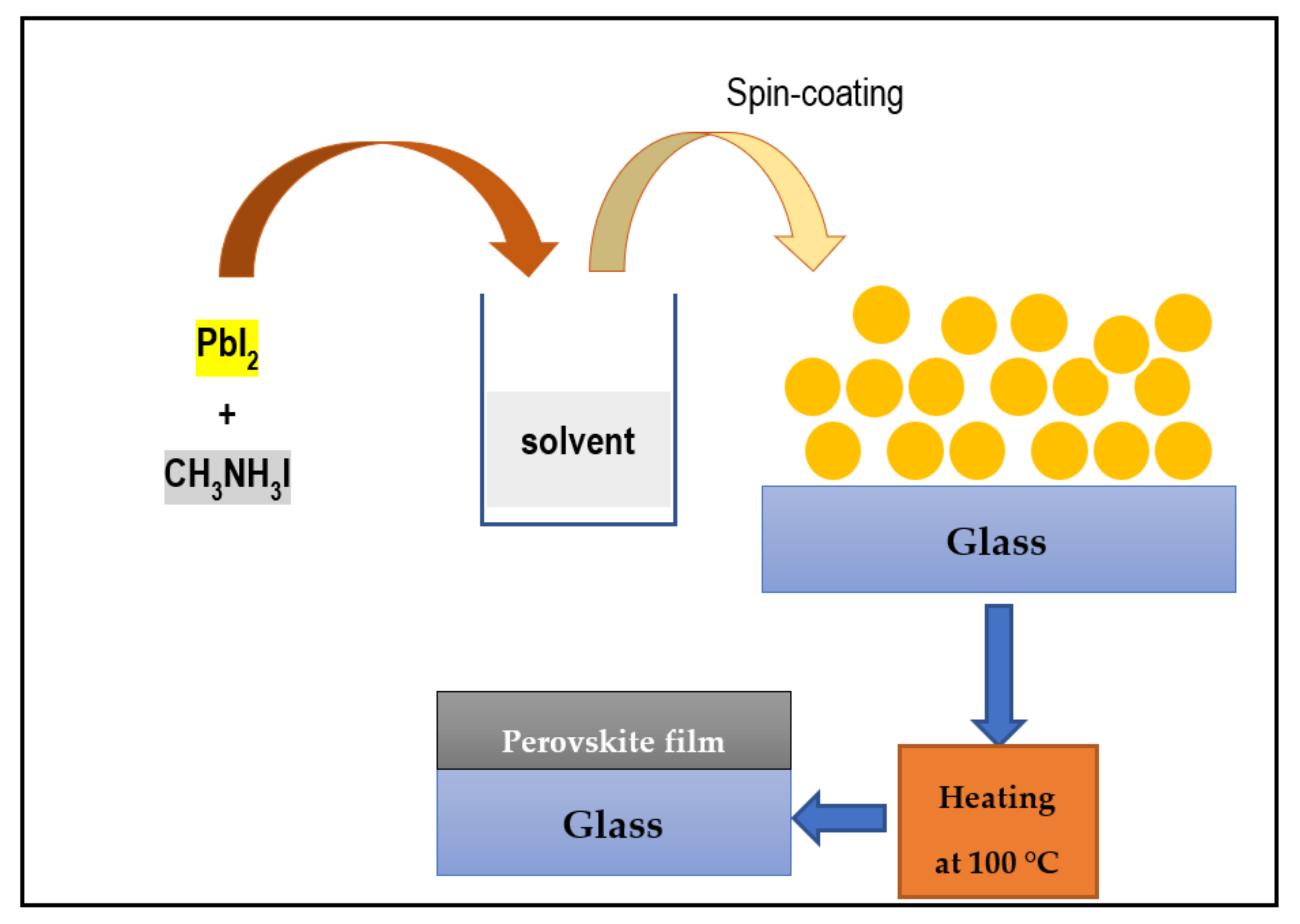
2.2. Methods
2.3. Characterization
3. Results
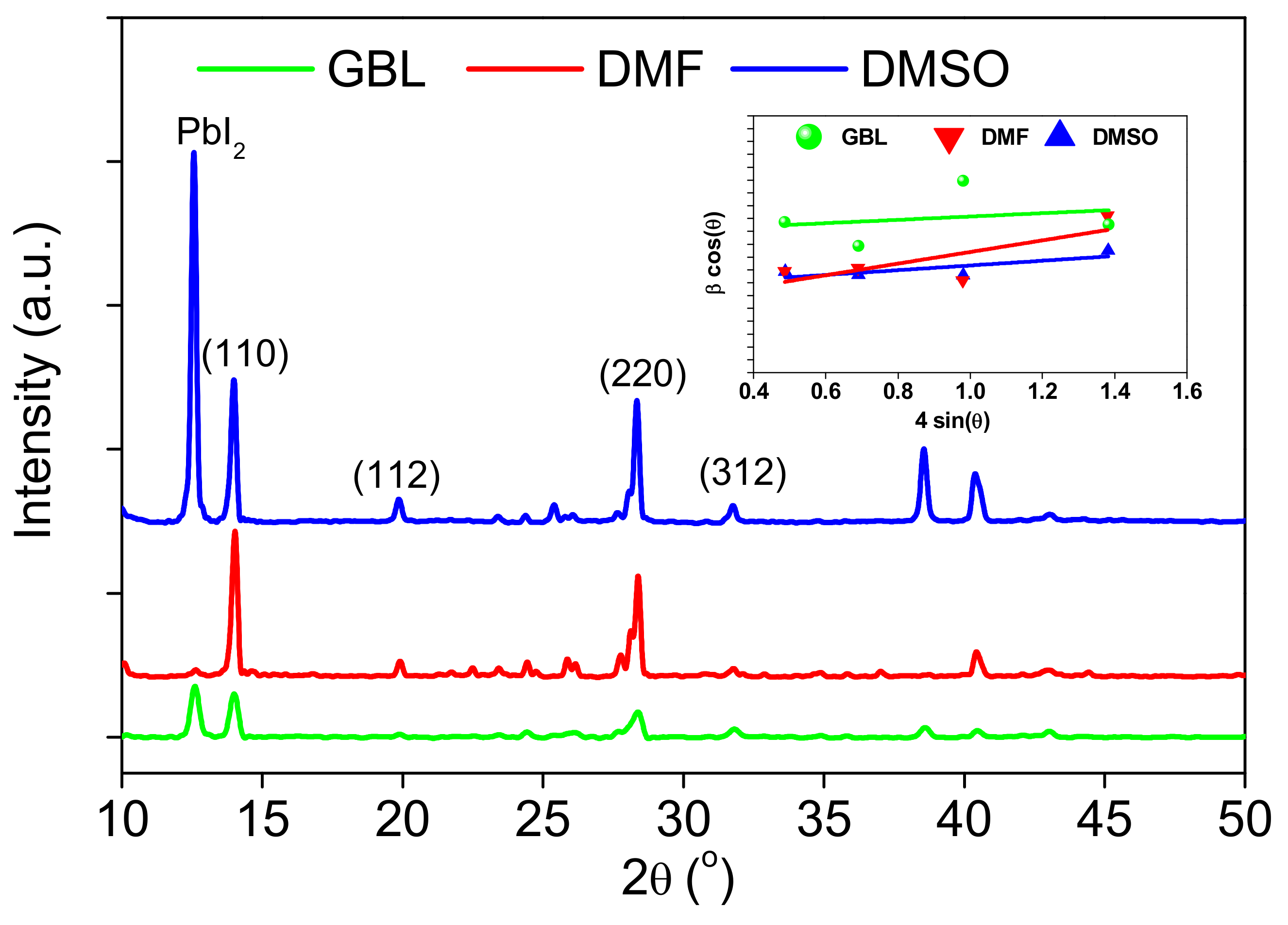
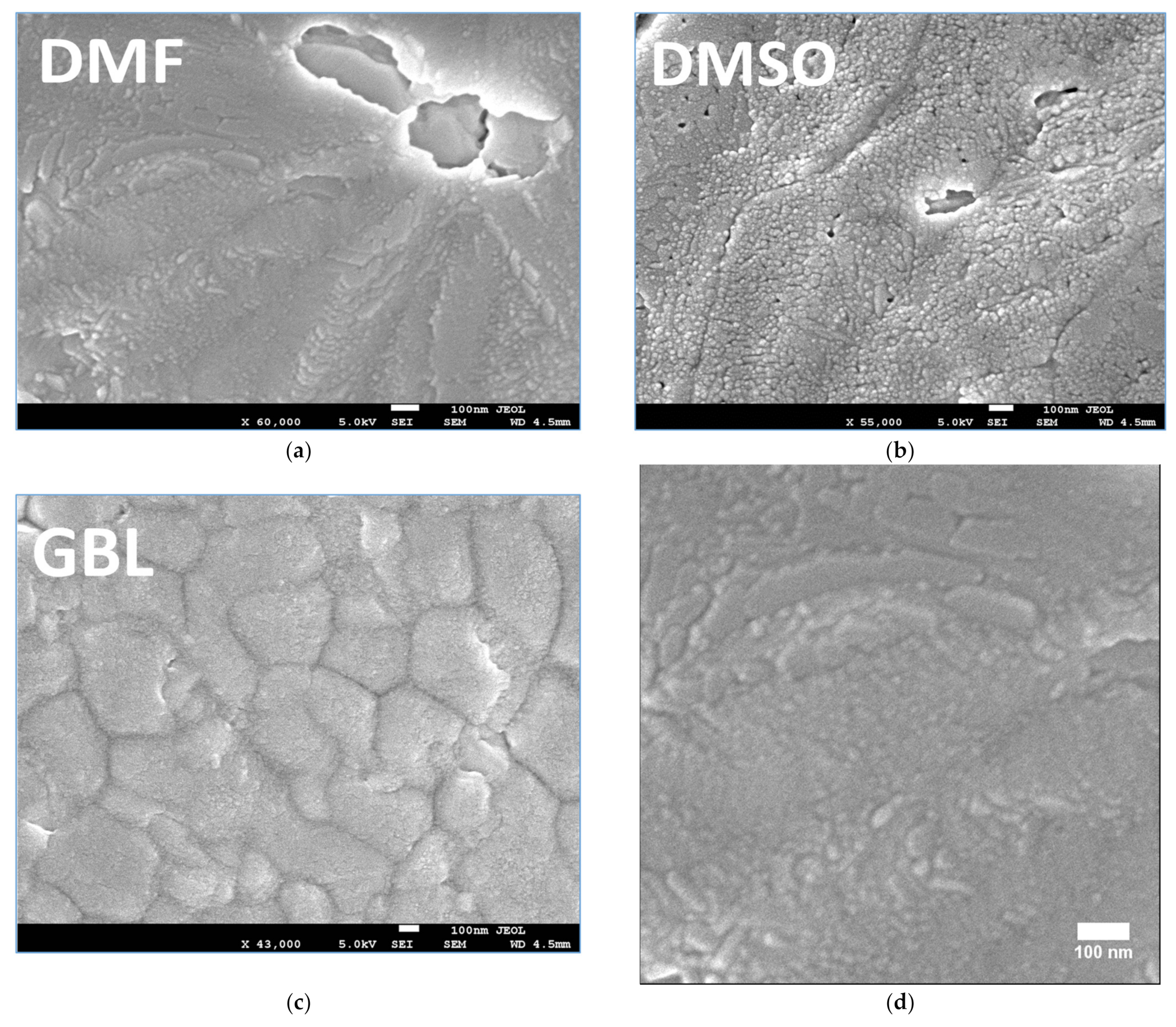
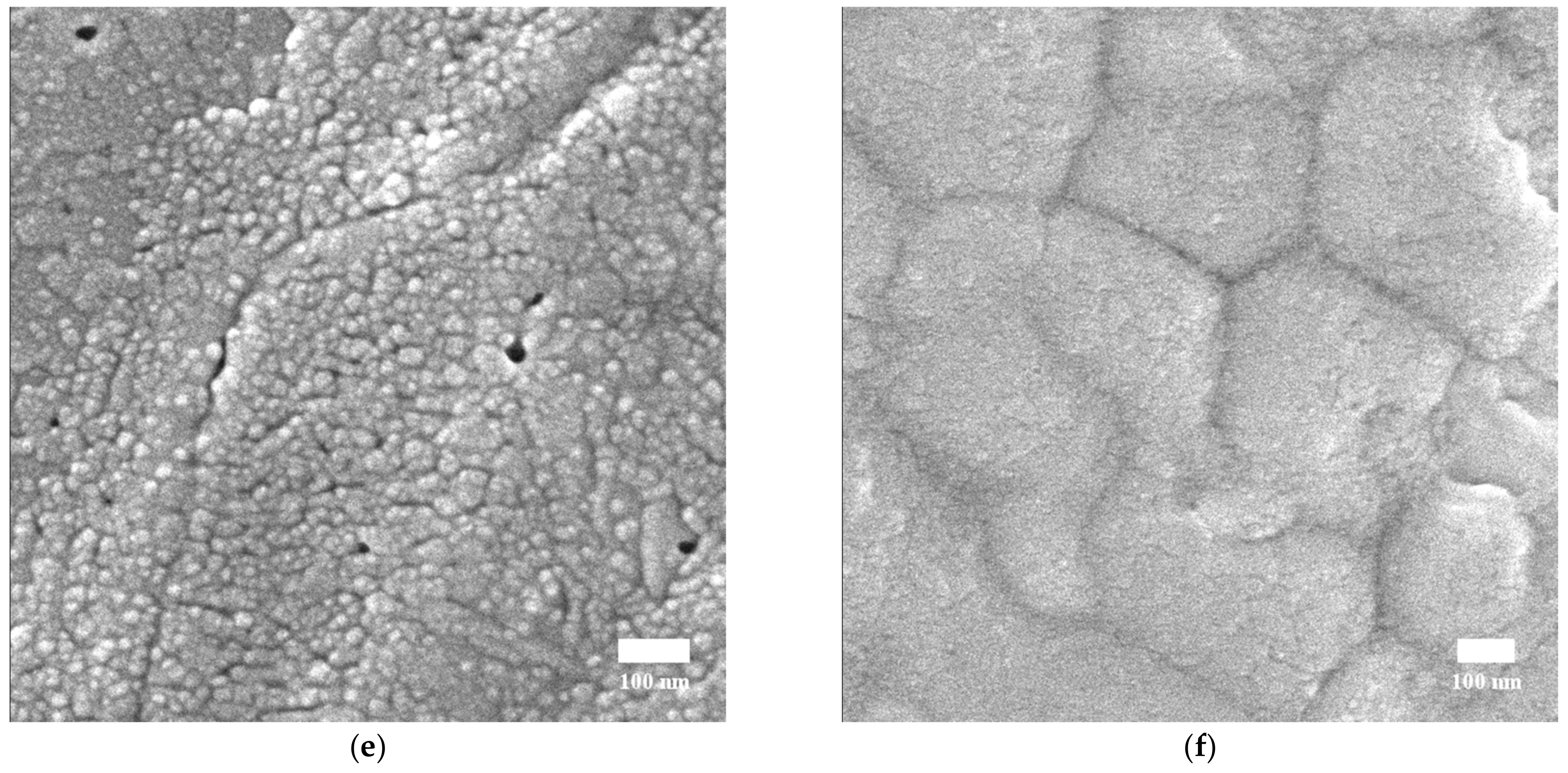
3.1. Structural Characteristics
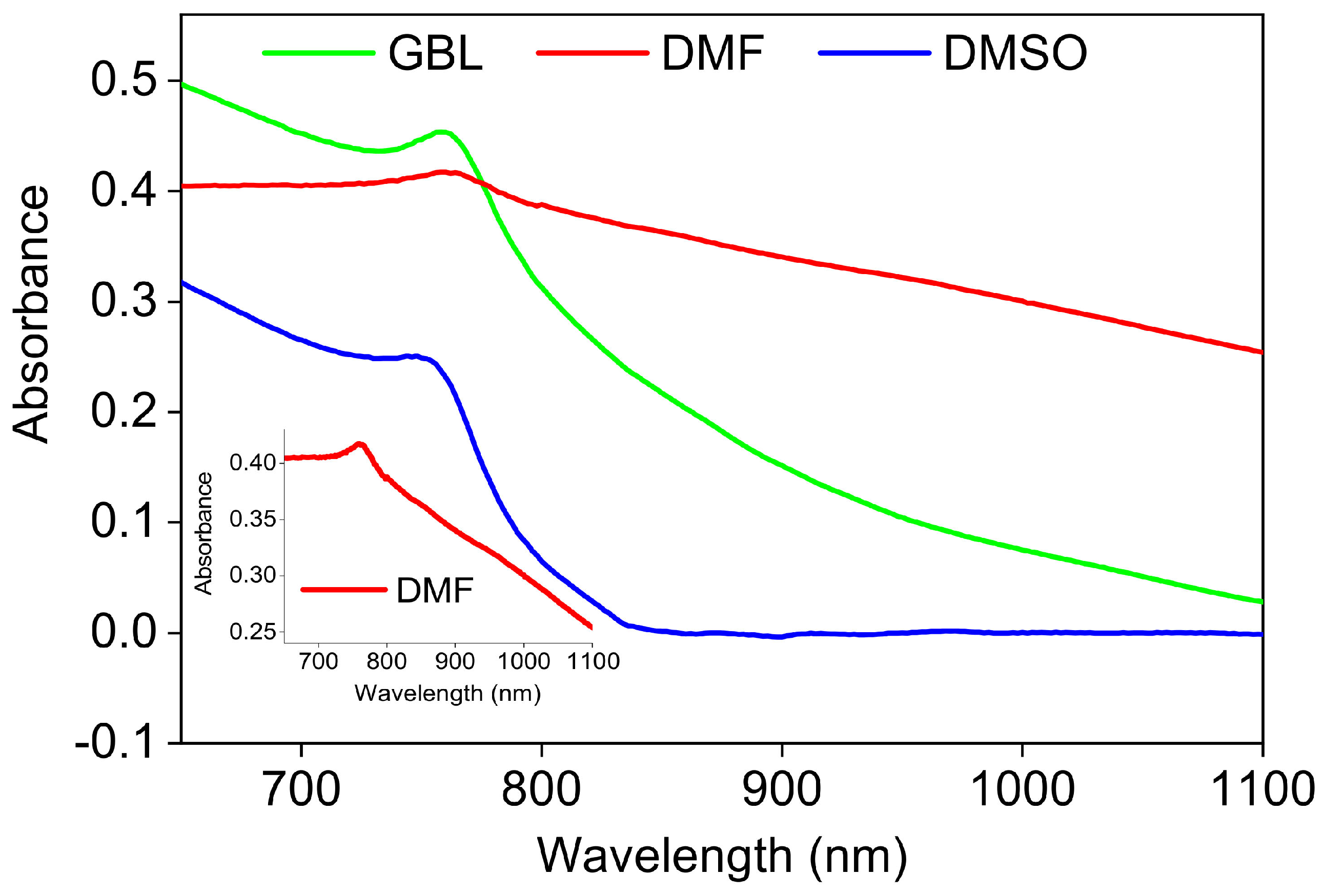
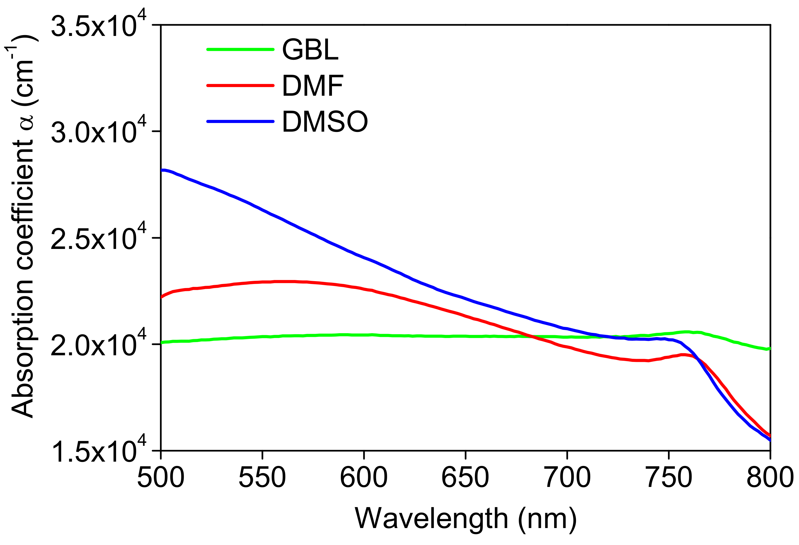
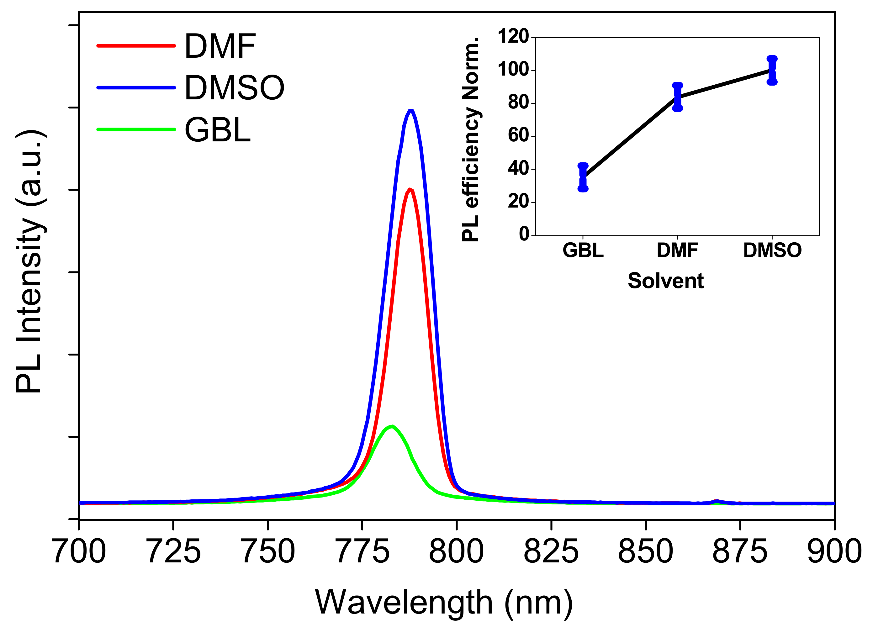
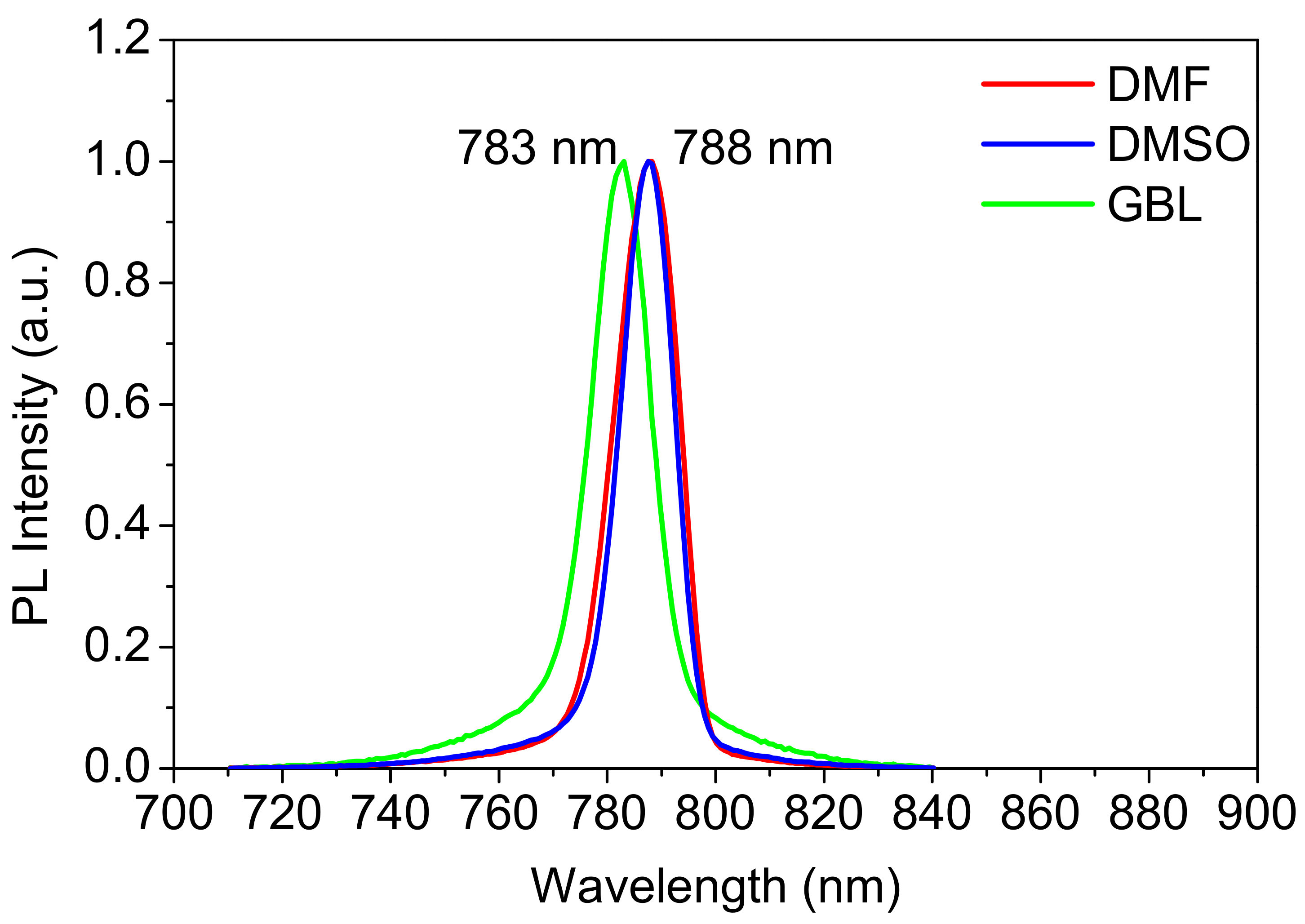
3.2. Optical Properties
4. Conclusions
Author Contributions
Funding
Institutional Review Board Statement
Informed Consent Statement
Data Availability Statement
Acknowledgments
Conflicts of Interest
References
- Yin, W.-J.; Shi, T.; Yan, Y. Unique properties of halide perovskites as possible origins of the superior solar cell performance. Adv. Mater. 2014, 26, 4653–4658. [Google Scholar] [CrossRef] [PubMed]
- Park, N.G. Organometal perovskite light absorbers toward a 20% efficiency low-cost solid-state mesoscopic solar cell. J. Phys. Chem. Lett. 2013, 4, 2423–2429. [Google Scholar] [CrossRef]
- Qaid, S.M.H.; Al Sobaie, M.S.; Majeed Khan, M.A.; Bedja, I.M.; Alharbi, F.H.; Nazeeruddin, M.K.; Aldwayyan, A.S. Band-gap tuning of lead halide perovskite using a single step spin-coating deposition process. Mater. Lett. 2016, 164, 498–501. [Google Scholar] [CrossRef]
- Alcocer, M.J.P.; Leijtens, T.; Herz, L.M.; Petrozza, A.; Snaith, H.J. Electron-hole diffusion lengths exceeding 1 micrometer in an organometal trihalide perovskite absorber. Science 2014, 342, 341–344. [Google Scholar]
- Adjokatse, S.; Fang, H.H.; Loi, M.A. Broadly tunable metal halide perovskites for solid-state light-emission applications. Mater. Today 2017, 20, 413–424. [Google Scholar] [CrossRef]
- Hirasawa, M.; Ishihara, T.; Goto, T.; Uchida, K.; Miura, N. Magnetoabsorption of the lowest exciton in perovskite-type compound (CH3NH3)PbI3. Phys. B 1994, 201, 427–430. [Google Scholar] [CrossRef]
- Tanaka, K.; Takahashi, T.; Ban, T.; Kondo, T.; Uchida, K.; Miura, N. Comparative study on the excitons in lead-halide-based perovskite-type crystals CH3NH3PbBr3 CH3NH3PbI3. Solid State Commun. 2003, 127, 619–623. [Google Scholar] [CrossRef]
- Ishihara, T. Optical properties of PbI-based perovskite structures. J. Lumin. 1994, 60–61, 269–274. [Google Scholar] [CrossRef]
- Shen, Q.; Ogomi, Y.; Chang, J.; Tsukamoto, S.; Kukihara, K.; Oshima, T.; Osada, N.; Yoshino, K.; Katayama, K.; Toyoda, T.; et al. Charge transfer and recombination at the metal oxide/CH3NH3PbClI2/spiro-OMeTAD interfaces: Uncovering the detailed mechanism behind high efficiency solar cells. Phys. Chem. Chem. Phys. 2014, 16, 19984. [Google Scholar] [CrossRef]
- Pang, S.; Chen, D. High-Quality Perovskite Film Preparations for Efficient Perovskite Solar Cells. In Emerging Solar Energy Materials; InTech: Houston, TX, USA, 2018; p. 217. [Google Scholar]
- Al-Asbahi, B.A.; Qaid, S.M.H.; Hezam, M.; Bedja, I.; Ghaithan, H.M.; Aldwayyan, A.S. Effect of deposition method on the structural and optical properties of CH3NH3PbI3 perovskite thin films. Opt. Mater. 2020, 103, 109836. [Google Scholar] [CrossRef]
- Eperon, G.E.; Burlakov, V.M.; Docampo, P.; Goriely, A.; Snaith, H.J. Morphological control for high performance, solution-processed planar heterojunction perovskite solar cells. Adv. Funct. Mater. 2014, 24, 151–157. [Google Scholar] [CrossRef]
- Mhamdi, A.; Mehdi, H.; Bouazizi, A. Effect of solvents and annealing treatment on the properties of the methylammonium lead tribromide perovskite thin films. J. Mater. Sci. Mater. Electron. 2021, 32, 2302–2311. [Google Scholar] [CrossRef]
- Mutlu, A.; Yeşil, T.; Zafer, C. Utilization of coordinating green solvents for high quality methylammonium bismuth iodide thin films for photovoltaic applications. Org. Electron. 2021, 95, 106191. [Google Scholar] [CrossRef]
- You, J.; Hong, Z.; Song, T.B.; Meng, L.; Liu, Y.; Jiang, C.; Zhou, H.; Chang, W.H.; Li, G.; Yang, Y. Moisture assisted perovskite film growth for high performance solar cells. Appl. Phys. Lett. 2014, 105, 183902. [Google Scholar] [CrossRef]
- Dualeh, A.; Tétreault, N.; Moehl, T.; Gao, P.; Nazeeruddin, M.K.; Grätzel, M. Effect of annealing temperature on film morphology of organic-inorganic hybrid pervoskite solid-state solar cells. Adv. Funct. Mater. 2014, 24, 3250–3258. [Google Scholar] [CrossRef]
- Burschka, J.; Pellet, N.; Moon, S.-J.; Humphry-Baker, R.; Gao, P.; Nazeeruddin, M.K.; Grätzel, M. Sequential deposition as a route to high-performance perovskite-sensitized solar cells. Nature 2013, 499, 316–319. [Google Scholar] [CrossRef]
- Jung, H.S.; Park, N.G. Perovskite solar cells: From materials to devices. Small 2015, 11, 10–25. [Google Scholar] [CrossRef]
- Liu, M.; Johnston, M.B.; Snaith, H.J. Efficient planar heterojunction perovskite solar cells by vapour deposition. Nature 2013, 501, 395–398. [Google Scholar] [CrossRef]
- Kim, B.-S.; Choi, M.-H.; Choi, M.-S.; Kim, J.-J. Composition-controlled organometal halide perovskite via CH3NH3I pressure in a vacuum co-deposition process. J. Mater. Chem. A 2016, 4, 5663–5668. [Google Scholar] [CrossRef]
- Song, T.; Chen, Q.; Zhou, H.; Jiang, C.; Wang, H.; Yang, M.; Liu, Y. Perovskite solar cells: Film formation and properties. J. Mater. Chem. A 2015, 3, 9032–9050. [Google Scholar] [CrossRef]
- Zhao, Y.; Zhu, K. CH3NH3Cl-assisted one-step solution growth of CH3NH3PbI3: Structure, charge-carrier dynamics, and photovoltaic properties of perovskite solar cells. J. Phys. Chem. C 2014, 118, 9412–9418. [Google Scholar] [CrossRef]
- Im, J.H.; Kim, H.S.; Park, N.G. Morphology-photovoltaic property correlation in perovskite solar cells: One-step versus two-step deposition of CH3NH3PbI3. APL Mater. 2014, 2, 081510. [Google Scholar] [CrossRef]
- Lv, S.; Pang, S.; Zhou, Y.; Padture, N.P.; Hu, H.; Wang, L.; Zhou, X.; Zhu, H.; Zhang, L.; Huang, C.; et al. One-step, solution-processed formamidinium lead trihalide (FAPbI(3−x)Clx) for mesoscopic perovskite–polymer solar cells. Phys. Chem. Chem. Phys. 2014, 16, 19206–19211. [Google Scholar] [CrossRef] [PubMed]
- Kim, H.-B.; Choi, H.; Jeong, J.; Kim, S.; Walker, B.; Song, S.; Kim, J.Y. Mixed solvents for the optimization of morphology in solution-processed, inverted-type perovskite/fullerene hybrid solar cells. Nanoscale 2014, 6, 6679. [Google Scholar] [CrossRef]
- Liu, R.; Xu, K. Solvent engineering for perovskite solar cells: A review. Micro Nano Lett. 2020, 15, 349–353. [Google Scholar] [CrossRef]
- Rong, Y.; Tang, Z.; Zhao, Y.; Zhong, X.; Venkatesan, S.; Graham, H.; Patton, M.; Jing, Y.; Guloy, A.M.; Yao, Y. Solvent engineering towards controlled grain growth in perovskite planar heterojunction solar cells. Nanoscale 2015, 7, 10595–10599. [Google Scholar] [CrossRef]
- Cai, B.; Zhang, W.H.; Qiu, J. Solvent engineering of spin-coating solutions for planar-structured high-efficiency perovskite solar cells. Cuihua Xuebao Chin. J. Catal. 2015, 36, 1183–1190. [Google Scholar] [CrossRef]
- Hwang, K.H.; Nam, S.H.; Kim, D.I.; Seo, H.J.; Boo, J.H. The influence of DMSO and ether via fast-dipping treatment for a perovskite solar cell. Sol. Energy Mater. Sol. Cells 2018, 180, 386–395. [Google Scholar] [CrossRef]
- Fang, X.; Wu, Y.; Lu, Y.; Sun, Y.; Zhang, S.; Zhang, J.; Zhang, W.; Yuan, N.; Ding, J. Annealing-free perovskite films based on solvent engineering for efficient solar cells. J. Mater. Chem. C 2017, 5, 842–847. [Google Scholar] [CrossRef]
- Liu, X.; Wu, J.; Yang, Y.; Wu, T.; Guo, Q. Pyridine solvent engineering for high quality anion-cation-mixed hybrid and high performance of perovskite solar cells. J. Power Sources 2018, 399, 144–150. [Google Scholar] [CrossRef]
- Wu, T.; Wu, J.; Tu, Y.; He, X.; Lan, Z.; Huang, M.; Lin, J. Solvent engineering for high-quality perovskite solar cell with an efficiency approaching 20%. J. Power Sources 2017, 365, 1–6. [Google Scholar] [CrossRef]
- Seo, J.; Park, S.; Chan Kim, Y.; Jeon, N.J.; Noh, J.H.; Yoon, S.C.; Seok, S. Il Benefits of very thin PCBM and LiF layers for solution-processed p–i–n perovskite solar cells. Energy Environ. Sci. 2014, 7, 2642–2646. [Google Scholar] [CrossRef]
- Jeon, N.J.; Noh, J.H.; Kim, Y.C.; Yang, W.S.; Ryu, S.; Seok, S. Il Solvent engineering for high-performance inorganic–organic hybrid perovskite solar cells. Nat. Mater. 2014, 13, 897–903. [Google Scholar] [CrossRef] [PubMed]
- Petrov, A.A.; Ordinartsev, A.A.; Fateev, S.A.; Goodilin, E.A.; Tarasov, A.B. Solubility of hybrid halide perovskites in dmf and dmso. Molecules 2021, 26, 7541. [Google Scholar] [CrossRef]
- Saianand, G.; Sonar, P.; Wilson, G.J.; Gopalan, A.I.; Roy, V.A.L.; Unni, G.E.; Mamun Reza, K.; Bahrami, B.; Venkatramanan, K.; Qiao, Q. Current advancements on charge selective contact interfacial layers and electrodes in flexible hybrid perovskite photovoltaics. J. Energy Chem. 2021, 54, 151–173. [Google Scholar] [CrossRef]
- Qaid, S.M.H.; Khan, M.N.; Alqasem, A.; Hezam, M.; Aldwayyan, A. Restraining effect of film thickness on the behaviour of amplified spontaneous emission from methylammonium lead iodide perovskite. IET Optoelectron. 2018, 13, 2–6. [Google Scholar] [CrossRef]
- Zuo, C.; Ding, L. Drop-casting to make efficient perovskite solar cells under high humidity. Angew. Chem. 2021, 133, 11342–11346. [Google Scholar] [CrossRef]
- Malinkiewicz, O.; Yella, A.; Lee, Y.H.; Espallargas, G.M.M.; Graetzel, M.; Nazeeruddin, M.K.; Bolink, H.J. Perovskite solar cells employing organic charge-transport layers. Nat. Photonics 2014, 8, 128–132. [Google Scholar] [CrossRef]
- Etgar, L.; Gao, P.; Xue, Z.; Peng, Q.; Chandiran, A.K.; Liu, B.; Nazeeruddin, M.K.; Grätzel, M. Mesoscopic CH3NH3PbI3/TiO2 heterojunction solar cells. J. Am. Chem. Soc. 2012, 134, 17396–17399. [Google Scholar] [CrossRef]
- Yao, Y.; Zou, X.; Cheng, J.; Ling, T.; Chang, C.; Chen, D. Influence of solution deposition process on modulating majority charge carrier type and quality of perovskite thin films for solar cells. Materials 2019, 12, 2494. [Google Scholar]
- Nath, D.; Singh, F.; Das, R. X-ray diffraction analysis by Williamson-Hall, Halder-Wagner and size-strain plot methods of CdSe nanoparticles- a comparative study. Mater. Chem. Phys. 2020, 239, 122021. [Google Scholar] [CrossRef]
- Qaid, S.M.; Ghaithan, H.M.; Al-Asbahi, B.A.; Aldwayyan, A.S. Tuning of amplified spontaneous emission wavelength for green and blue light emission through the tunable composition of CsPb(Br1–xClx)3 inorganic perovskite quantum dots. J. Phys. Chem. C 2021, 125, 9441–9452. [Google Scholar] [CrossRef]
- Thompson, C.V.; Carel, R. Stress and grain growth in thin films. J. Mech. Phys. Solids 1996, 44, 657–673. [Google Scholar] [CrossRef]
- Qaid, S.M.H.; Al-Asbahi, B.A.; Ghaithan, H.M.; Aldwayyan, A.S. Tuning the optical properties of meh–ppv/pfo hybrid thin films via the incorporation of cspbbr3 quantum dots. Coatings 2021, 11, 154. [Google Scholar] [CrossRef]
- Adhikari, G.C.; Thapa, S.; Yue, Y.; Zhu, H.; Zhu, P. Near unity plqy and high stability of barium thiocyanate based all-inorganic perovskites and their applications in white light-emitting diodes. Photonics 2021, 8, 209. [Google Scholar] [CrossRef]
- Maharaz, M.N.; Halimah, M.K.; Paiman, S.; Saiden, N.M.; Alibe, I.M. Influence of solvents and irradiation time on structural and optical properties of cubic PbS nanoparticles. Int. J. Electrochem. Sci. 2018, 13, 9317–9332. [Google Scholar] [CrossRef]
- Liu, Y.; Yang, Z.; Liu, S.F. Recent progress in single-crystalline perovskite research including crystal preparation, property evaluation, and applications. Adv. Sci. 2018, 5, 1700471. [Google Scholar] [CrossRef]
- Saidaminov, M.I.; Abdelhady, A.L.; Maculan, G.; Bakr, O.M. Retrograde solubility of formamidinium and methylammonium lead halide perovskites enabling rapid single crystal growth. Chem. Commun. 2015, 51, 17658–17661. [Google Scholar] [CrossRef]
- Cao, Y.; Hu, P.; Jia, D. Solvothermal synthesis, growth mechanism, and photoluminescence property of sub-micrometer PbS anisotropic structures. Nanoscale Res. Lett. 2012, 7, 668. [Google Scholar] [CrossRef]
- Alagumuthu, G.; Kirubha, R. Synthesis and characterisation of silver nanoparticles in different medium. Open J. Synth. Theory Appl. 2012, 1, 13–17. [Google Scholar] [CrossRef][Green Version]
- Sathyamoorthy, R.; Kungumadevi, L. Facile synthesis of PbS nanorods induced by concentration difference. Adv. Powder Technol. 2015, 26, 355–361. [Google Scholar] [CrossRef]
- Kumar, S.A.; Saravanan, V.; Rajasimman, M. Microwave mediated synthesis and characterizations of CdO nanoparticles. J. Adv. Chem. Sci. 2015, 1, 133–138. [Google Scholar]
- Londoño-Restrepo, S.M.; Jeronimo-Cruz, R.; Millán-Malo, B.M.; Rivera-Muñoz, E.M.; Rodriguez-García, M.E. Effect of the nano crystal size on the X-ray diffraction patterns of biogenic hydroxyapatite from human, bovine, and porcine bones. Sci. Rep. 2019, 9, 5915. [Google Scholar] [CrossRef] [PubMed]
- Adhikari, G.C.; Vargas, P.A.; Zhu, H.; Grigoriev, A.; Zhu, P. Tetradic phosphor white light with variable CCT and superlative CRI through organolead halide perovskite nanocrystals. Nanoscale Adv. 2019, 1, 1791–1798. [Google Scholar] [CrossRef]
- Zhang, L.; Zuo, C.; Ding, L. Efficient MAPbI3 solar cells made via drop-coating at room temperature. J. Semicond. 2021, 42, 072201. [Google Scholar] [CrossRef]
- Yanagida, M.; Shirai, Y.; Khadka, D.B.; Miyano, K. Photoinduced ion-redistribution in CH3NH3PbI3 perovskite solar cells. Phys. Chem. Chem. Phys. 2020, 22, 25118–25125. [Google Scholar] [CrossRef]
- Ghaithan, M.H.; Qaid, S.M.H.; Alahmed, Z.A.; Hezam, M.; Lyras, A.; Amer, M.; Aldwayyan, A.S. Anion substitution effects on the structural, electronic, and optical properties of inorganic CsPb(I1–xBrx)3 and CsPb(Br1–xClx)3 perovskites: Theoretical and experimental approaches. J. Phys. Chem. C 2021, 125, 886–897. [Google Scholar] [CrossRef]
- Al Mohaimeed, R.M.; Ansari, A.A.; Aldwayyan, A. The role of solvent environment on the optical behavior of chemically synthesized silicon nanoparticles. J. Spectrosc. 2018, 2018, 6870645. [Google Scholar] [CrossRef]
- Khan, M.N.; Khan, M.A.M.; Al Dwayyan, A.S.; Labis, J.P.; Yu, W.W. Comparative study on electronic, emission, spontaneous property of porous silicon in different solvents. J. Nanomater. 2014, 2014, 682571. [Google Scholar] [CrossRef]
- Adhikari, G.C.; Thapa, S.; Zhu, H.; Zhu, P. UV resin enhanced stability of metal halide perovskite nanocrystals for white light-emitting diodes. ACS Appl. Electron. Mater. 2020, 2, 35–40. [Google Scholar] [CrossRef]
- Kojima, A.; Teshima, K.; Shirai, Y.; Miyasaka, T. Organometal halide perovskites as visible-light sensitizers for photovoltaic cells. J. Am. Chem. Soc. 2009, 131, 6050–6051. [Google Scholar] [CrossRef] [PubMed]


| Name | Abbreviation | Formula | Density (g·mL−1) | Dipole Moment (Polarity) (Debye) |
|---|---|---|---|---|
| Dimethylformamide | DMF | C3H7NO | 0.948 | 3.86 |
| Dimethyl sulfoxide | DMSO | C2H6OS | 1.1004 | 3.96 |
| γ-Butyrolactone | GBL | C4H6O2 | 1.1296 | 4.27 |
| Solvent | D (nm) | Micro Strain ε × 10–4 | Dislocation Density δ × 10−3 (nm)−4 |
|---|---|---|---|
| DMF | 56.82 | 22.60 | 3.10 |
| DMSO | 42.65 | 9.21 | 5.50 |
| GBL | 25.52 | 6.46 | 15.35 |
| Optical Parameter | DMF | DMSO | GBL |
|---|---|---|---|
| 761 | 750 | 759 | |
| 1.96 | 1.99 | 2.06 | |
| 0.51 | 0.50 | 0.94 | |
| 1.623 | 1.632 | 1.625 | |
| PL Peak (nm) | 787.7 | 787.9 | 782.5 |
| ASE Peak (nm) | 789.5 | 788.2 | 783.5 |
| ASE FWHM (nm) | 11.19 | 13.98 | 13.43 |
Publisher’s Note: MDPI stays neutral with regard to jurisdictional claims in published maps and institutional affiliations. |
© 2022 by the authors. Licensee MDPI, Basel, Switzerland. This article is an open access article distributed under the terms and conditions of the Creative Commons Attribution (CC BY) license (https://creativecommons.org/licenses/by/4.0/).
Share and Cite
Qaid, S.M.H.; Ghaithan, H.M.; Al-Asbahi, B.A.; Aldwayyan, A.S. Solvent Effects on the Structural and Optical Properties of MAPbI3 Perovskite Thin Film for Photovoltaic Active Layer. Coatings 2022, 12, 549. https://doi.org/10.3390/coatings12050549
Qaid SMH, Ghaithan HM, Al-Asbahi BA, Aldwayyan AS. Solvent Effects on the Structural and Optical Properties of MAPbI3 Perovskite Thin Film for Photovoltaic Active Layer. Coatings. 2022; 12(5):549. https://doi.org/10.3390/coatings12050549
Chicago/Turabian StyleQaid, Saif M. H., Hamid M. Ghaithan, Bandar Ali Al-Asbahi, and Abdullah S. Aldwayyan. 2022. "Solvent Effects on the Structural and Optical Properties of MAPbI3 Perovskite Thin Film for Photovoltaic Active Layer" Coatings 12, no. 5: 549. https://doi.org/10.3390/coatings12050549
APA StyleQaid, S. M. H., Ghaithan, H. M., Al-Asbahi, B. A., & Aldwayyan, A. S. (2022). Solvent Effects on the Structural and Optical Properties of MAPbI3 Perovskite Thin Film for Photovoltaic Active Layer. Coatings, 12(5), 549. https://doi.org/10.3390/coatings12050549