Article

Effect of Seed Layer on the Growth of Zinc Oxide Nanowires by Chemical Bath Deposition Method

by
Zaidatul Hanis Azmi
1,
Siti Nurnadiah Mohd Aris
1,
Shamsu Abubakar
1,
Suresh Sagadevan
2,
Rikson Siburian
3 and
Suriati Paiman
1,4,*
1
Department of Physics, Faculty of Science, Universiti Putra Malaysia, Serdang 43400, Malaysia
2
Nanotechnology & Catalysis Research Centre, University of Malaya, Kuala Lumpur 50630, Malaysia
3
Department of Chemistry, Faculty of Mathematics and Natural Sciences, Universitas Sumatera Utara, Medan 20155, Indonesia
4
Functional Nanotechnology Devices Laboratory (FNDL), Institute of Nanoscience and Nanotechnology, Universiti Putra Malaysia, Serdang 43400, Malaysia
*
Author to whom correspondence should be addressed.
Coatings 2022, 12(4), 474; https://doi.org/10.3390/coatings12040474
Submission received: 18 February 2022 / Revised: 9 March 2022 / Accepted: 15 March 2022 / Published: 31 March 2022
(This article belongs to the Special Issue Optical Thin Films: Preparation, Application and Development)

Abstract

:
This study concentrated on the effect of the ZnO seed layer on the growth of ZnO nanowires by the chemical bath deposition method. Multilayer coatings were used to control the thickness of the seed layer of one layer, three layers, and five layers. The seed layer thickness was measured using a profilometer at 14.43, 33.31, and 53.13 nm for one-layer, three-layer, and five-layer samples, respectively. The samples were then immersed in a chemical bath deposition solution at 90 °C for 3 h to allow ZnO nanowires to grow. The X-ray diffraction (XRD) pattern of seed layers revealed a polycrystalline wurtzite structure with (101) orientation as the dominant peak in all samples. Field emission scanning electron microscopy (FESEM) revealed that ZnO nanowires grown in a single layer have a flower-like structure, whereas ZnO nanowires grown in three and five layers have a rod-like structure. Further, ImageJ software revealed that the diameter and length of the ZnO nanowires were in the 40–90 nm and 100–900 nm ranges, respectively. The five-layer sample had the highest density of ZnO nanowires at 668 µm−2, followed by the three-layer sample and the one-layer sample. However, the ZnO nanowires in the five-layer and one-layer samples are not vertically aligned. On the other hand, the three-layer sample had the best vertical alignment of this group of samples.

1. Introduction

One-dimensional (1D) nanostructures have been extensively studied because of their potential applications in nanoelectronic devices such as field-effect transistors, single-electron transistors, photodiodes, and chemical sensors [1,2,3]. At room temperature, zinc oxide (ZnO) has a large bandgap (3.37 eV) and a high excitation binding energy (60 meV) [4]. As a result, 1D ZnO nanorods can be used in a variety of applications, such as ultraviolet light-emitting devices, field-effect transistors, solar cells, and chemical sensors [5]. To deposit the ZnO seed layer, various fabrication techniques have been used. However, because of the sophisticated equipment setup, the cost of techniques is high, making them unsuitable for commercial production of ZnO nanowires for various applications. Direct bandgap properties and a room temperature excitation binding energy of 60 meV found in ZnO [6,7,8] demonstrate simultaneous evidence of high electrical, optical, and piezoelectric performance, establishing the applications of ZnO in the fields of piezoelectric transducers, photovoltaic solar cell devices, gas sensors, biosensors, transistors, optoelectronic, and, more recently, nanogenerator technologies [9]. ZnO nanorods (NRs) are an example of nanostructured materials that have received much attention. Because of their large surface area to volume ratio, high sensitivity to adsorbed molecules on their surfaces, and good electric transport properties, ZnO NRs have shown great promise as UV sensors due to their wide bandgap, visible light sensitivity (in the case of high-quality NRs), low cost, and ease of nanostructure fabrication. Furthermore, the importance of a seed layer in the production of ZnO nanowires has been reported earlier [10]. According to these findings, ZnO nanowires grown from a seed layer using sol-gel have a higher quality than seedless ZnO [10]. Another study from Fang’s group demonstrates that ZnO nanowires cannot be grown directly from Si substrates [11]. Several groups [12,13,14] have reported the effect of the ZnO seed layer on catalyst-free growth of ZnO nanorods and their morphology, crystallinity, and diameter using various methods. The structural quality of the nanorods was heavily influenced by the crystalline quality of the ZnO seed layer. Most synthesized nanorods were not aligned, limiting their applications in nanoscale electronic and optoelectronic devices. As a result, controlled and well-aligned growth of ZnO nanorod arrays is critical. The key factors for the well-aligned vertical growth of ZnO nanorods are an ultrathin layer and uniform distribution of ZnO seed in the ZnO layer. Zhao et al. [15] reported the high-temperature growth of vertically aligned ZnO nanorods on Si using a thin ZnO seed layer. However, the effects of growth temperature, substrate material, and overall nanorod quality have not been investigated. In other words, the ZnO seed layer is critical in the production of ZnO nanowires. Researchers have agreed that the ZnO seed condition plays a significant role in controlling the growth of nanowires. The seed layer thickness, annealing temperature, and precursor concentration are some of the seed conditions that may arise from the ZnO nanowire properties [16,17]. The thickness of the ZnO seed layer influences the growth of ordered ZnO nanorods as well as their density, which may affect dye-sensitized solar cells [18]. Another study found that the seed layer thickness can influence the alignment of ZnO nanorods [19]. A thicker seed layer results in poorly aligned ZnO nanorods, whereas a thinner seed layer results in vertically aligned ZnO nanorods [19]. As a result, it is concluded that the seed layer thickness influences the growth of ZnO nanowires. There is widespread agreement that the seed layer serves as a template for the growth of ZnO nanowires. Numerous techniques, including pulsed laser deposition, catalytic growth via a vapor–liquid–solid epitaxial mechanism, and physical vapor deposition, have been used to synthesize ZnO nanowires [20]. However, in recent years, there has been much focus on the chemical route technique known as chemical bath deposition (CBD). The technique is a low-cost, simple thin-film process that can synthesize substrates of various shapes and sizes. As a result, using chemical bath deposition to synthesize ZnO nanowires is of interest. Several researchers discovered that many significant parameters such as precursor concentration, growth temperature, seed layer type, and seed layer thickness influenced the formation of ZnO nanowires [13].
Taking these important factors into account, it is well known that the thickness of the ZnO seed layer is key for well-aligned ZnO nanowires. The present study sought to clarify the significance of growth surfaces of varying thicknesses in the fabrication of vertically aligned ZnO nanowires. Further, the effect of these multilayer films on morphological and structural properties is investigated. The contribution of surface roughness to the alignment of ZnO nanowires is discussed in detail.

2. Materials and Methods

2.1. Substrate Preparation

A silicon wafer was cleaved using a diamond cutter to form a smaller substrate, which was then sonicated with isopropyl alcohol and acetone alternately and rinsed in deionized water (DI water). The substrate then finally was left to dry. The purpose of cleaning the substrate is to prevent contamination from other impurities.

2.2. Spin Coating Technique

The resultant sol was employed to fabricate the thin film by the spin-coating process after 12 h of aging. The sol-gel solution was dropped onto Si substrate until covering the surface (with approximation of 100 μL). The substrate then was rotated at a spin-coating speed of 3000 rpm for 30 s by using a P-6708D series spin coater (Specialty Coating Systems Inc, Indianapolis, IN, United States). The sample was then left to dry at 100 °C from room temperature for 10 min on a hot plate. The process was repeated according to parameters of one layer, three layers, and five layers.

2.3. Synthesis of ZnO Nanowires by Chemical Bath Solution

The CBD method was used to grow nanowires from seed-coated Si samples. For this purpose, 50 mL of deionized (DI) water was used to prepare equimolar aqueous solutions of 0.03 M zinc nitrate hexahydrate (Zn(NO3)2·6H2O) and hexamethylenetetramine (HMTA: C6H12N4). Each solution was placed on the stirrer for 10 min before being mixed. After combining zinc nitrate hexahydrate and HMTA, a clear, transparent solution was formed. A relevant chemical equation for ZnO formation is shown below.
Decomposition reaction:
(CH2)6N4 + 6H2O → 6HCHO + 4NH3
Hydroxyl supply reaction:
NH3 + H2O ↔ NH4+ + HO
Supersaturation reaction:
Zn2+ + 2OH ↔ Zn (OH)2
ZnO nanowire growth reaction:
Zn (OH)2 ↔ ZnO + H2O
Nucleation and particle growth mechanisms are involved in the formation of ZnO nanostructures. Nucleation is the breakdown of a collection of molecules and particle combinations to form a film of a certain thickness on the surface of a sample through a heterogeneous reaction. Formaldehyde and NH3 are formed during the thermal decomposition of HMTA (reaction (1)). The ammonia produced then reacts with water to produce OH ion, which is then used in the next reaction with Zn2+. The supersaturation reaction (reaction (2)) is one of the most important stages in the formation of ZnO nanowires, which later decompose into solid ZnO with increasing temperature and time via the dehydration reaction (reaction (3)).

2.4. Growth of ZnO Nanowires by Using Chemical Bath Deposition

Using a sample holder, the ZnO seed layer prepared substrate was dipped vertically in the chemical bath solution. To ensure contamination, the beaker containing the chemical bath solution and silicon substrates was covered with aluminum foil. After that, all of the samples were placed in a 90 °C oven for 3 h. Following growth, the samples were rinsed with DI water to remove excess salt from the surface and air-dried. After some time, the chemical bath solution was transformed from a clear, transparent solution to a white turbid (milky) transparent solution. On the other hand, the sample had a white precipitate on the top surface. During the dipping of the ZnO seed layer in the bath solution, microscope glass slides and masking tape were used to ensure the vertical position was achieved for optimum growth of nanowires.

2.5. Seed Layer Annealing

The seed-coated sample was then placed in the furnace for the purpose of annealing at the optimum time of 3 h using a low-temperature furnace. The time of the rise in temperature from room temperature of 30 °C was set to 1 h. The next 1 h was set for a constant temperature of 300 °C, and another an hour was set for decreasing temperature back to room temperature.

2.6. Characterization Techniques

The orientation and crystalline structure of the ZnO nanowires were determined by X-ray diffraction (XRD) with the Philips (Amsterdam, The Netherlands) brand PW 3040/60 MPD X’Pert High 25 Pro 21 PAN-Analytical. The X-ray radiation source used was CuKα of wavelength λ = 1.54056 Å operating at 40 keV and 100 mA. AFM tips (Bruker Nano Surfaces, Tucson, AZ, United States) were used with a spring constant of 0.4 N/m and resonance frequencies of 70 kHz. Image analysis for this characterization was completed with NanoDrive Dimension Edge software (version 8.06). The field emission scanning electron microscope (FESEM, FEI, Hillsboro, OR, United State) instrument used was a Nova NanoSEM 230. The parameters used were 10.0 kV accelerating voltage, 12.5 μA emission current, 3.0 probe current (spot size), and slow capture scan. ImageJ software (version 1.53) was used to determine the diameter, length, and thickness of the nanowire. A profilometer was used to measure the thickness of seed layer ZnO after the annealing process. The model used was as follows: XP-200 Stylus, AMBIOS Profilometer, scan speed set to 0.20 mm/s, and scan length of 5 mm.

2.7. Thickness of ZnO Seed Layer

Table 1 shows the thickness of the seed layer as measured using a profilometer on one-layer, three-layer, and five-layer samples. According to the table, increasing the number of ZnO layers during the sol-gel spin coating process resulted in a thicker seed layer. The rising trend is due to an increase in ZnO adatoms (adsorbed atoms). More ZnO adatoms are deposited to the substrate as the number of coatings increases, resulting in a thicker and denser seed layer on top of the substrate. The obtained results support the use of multilayer coating to increase the thickness of the seed layer.

3. Results and Discussion

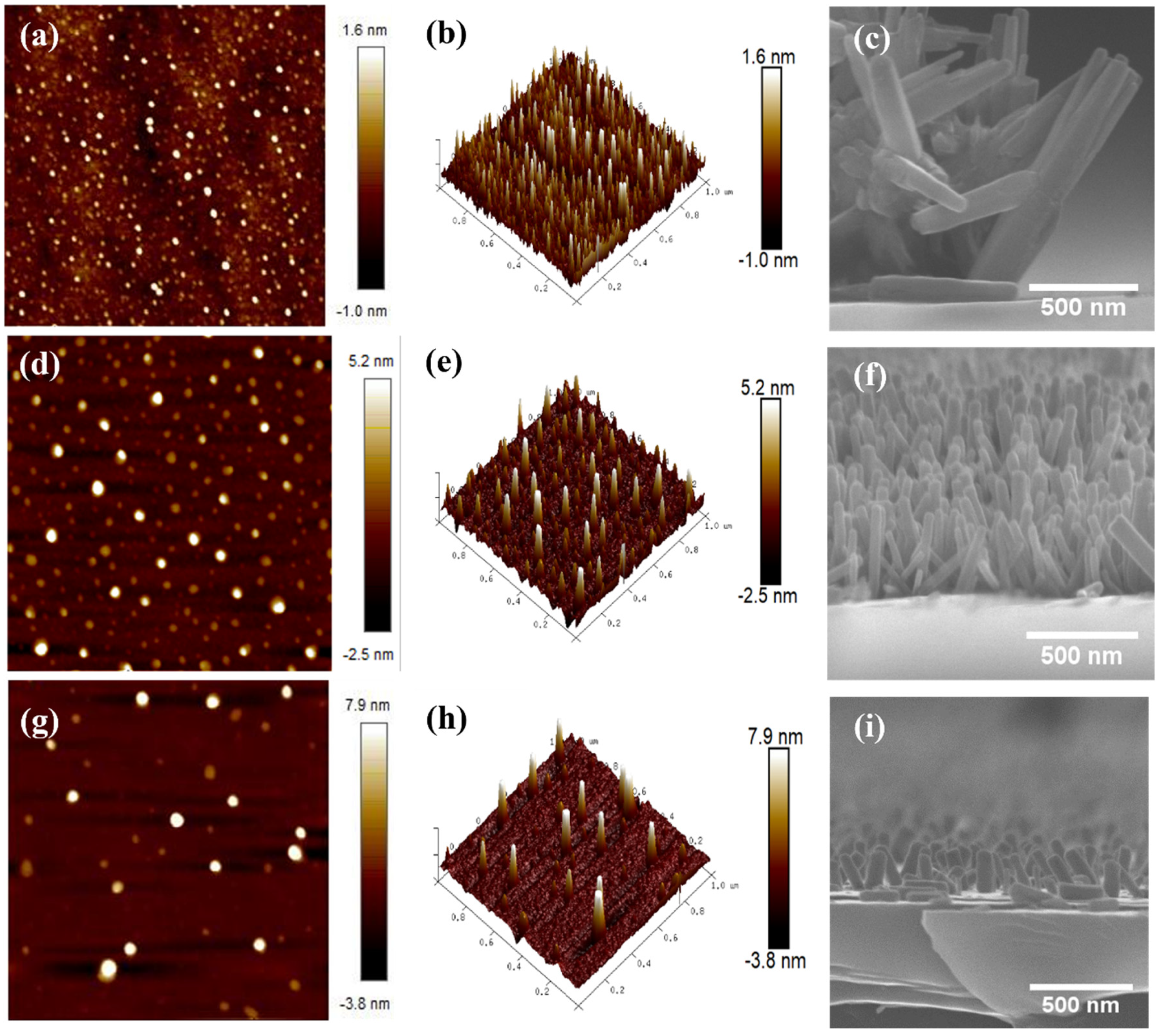
3.1. Crystallinity of ZnO Seed Layer and ZnO Nanowires

The crystallinity and preferred growth orientation of the ZnO seed layer deposited on Si substrate were determined using XRD. Figure 1a depicts the XRD pattern of a ZnO seed layer, whereas Figure 1b depicts the XRD of ZnO nanowires. In all samples, a dominant peak at 2θ = 36.25° is observed, which is associated with the (101) crystalline structure, indicating the preferable orientation for both the deposited ZnO seed layer and the ZnO nanowires. Aside from the diffraction peak at (101), other peaks at (100) and (002) were observed, indicating that ZnO has a polycrystalline structure. The relative intensity of these peaks increases obviously with an increase in ZnO seed layer thickness from a one-layer sample to a five-layer sample. In addition, XRD peaks in ZnO nanowires are much sharper than XRD peaks in the ZnO seed layer due to size crystallite size. The high intensity of XRD could be attributed to the crystallinity of the ZnO. As the coating layer thickness increases, so does the presence of ZnO adatoms, resulting in a high number of individual crystallite domains in phase. In addition, an extra phase of (201) and (112) is observed in ZnO nanowires. This is thought to be due to crystallinity, as reported [21].
However, the one-layer sample in Figure 1a has the lowest XRD intensity when compared to the three-layer and five-layer samples. This is thought to be due to the seed layer’s lower density of ZnO adatoms. As a result of the limited number of ZnO particles in the one-layer sample, the XRD ray scanning cannot be performed well [22]. Furthermore, the intensity of the one-layer sample increases for ZnO nanowires, indicating an improvement in crystallinity. All of the observed diffraction peaks can be well indexed to this phase with the wurtzite ZnO structure (JCPDS card No. 36-1451) as the reference, with the lattice parameter of ZnO being a = 3.250 Å, c = 5.207 Å, and c/a = 1.6. The absence of impurity peaks in the obtained pattern confirms the high purity of the synthesized product. Additionally, the crystalline size of the sample was calculated using Scherrer’s formula:
D = 0.94 λ β cos θ
where k is the Scherrer constant, considered to have the value ~0.89; λ is the wavelength used for the diffraction; β is the full width at half maximum; and θ is the diffraction angle. The full width at half maximum (FWHM) value of the (101) plane with different seed layer thickness is shown in Table 2. According to the results, as the seed layer thickness increases, so does the FWHM value and thus the crystallite size. The results confirmed that the ZnO seed layer in the five-layer sample has the highest crystallinity of the sample set.

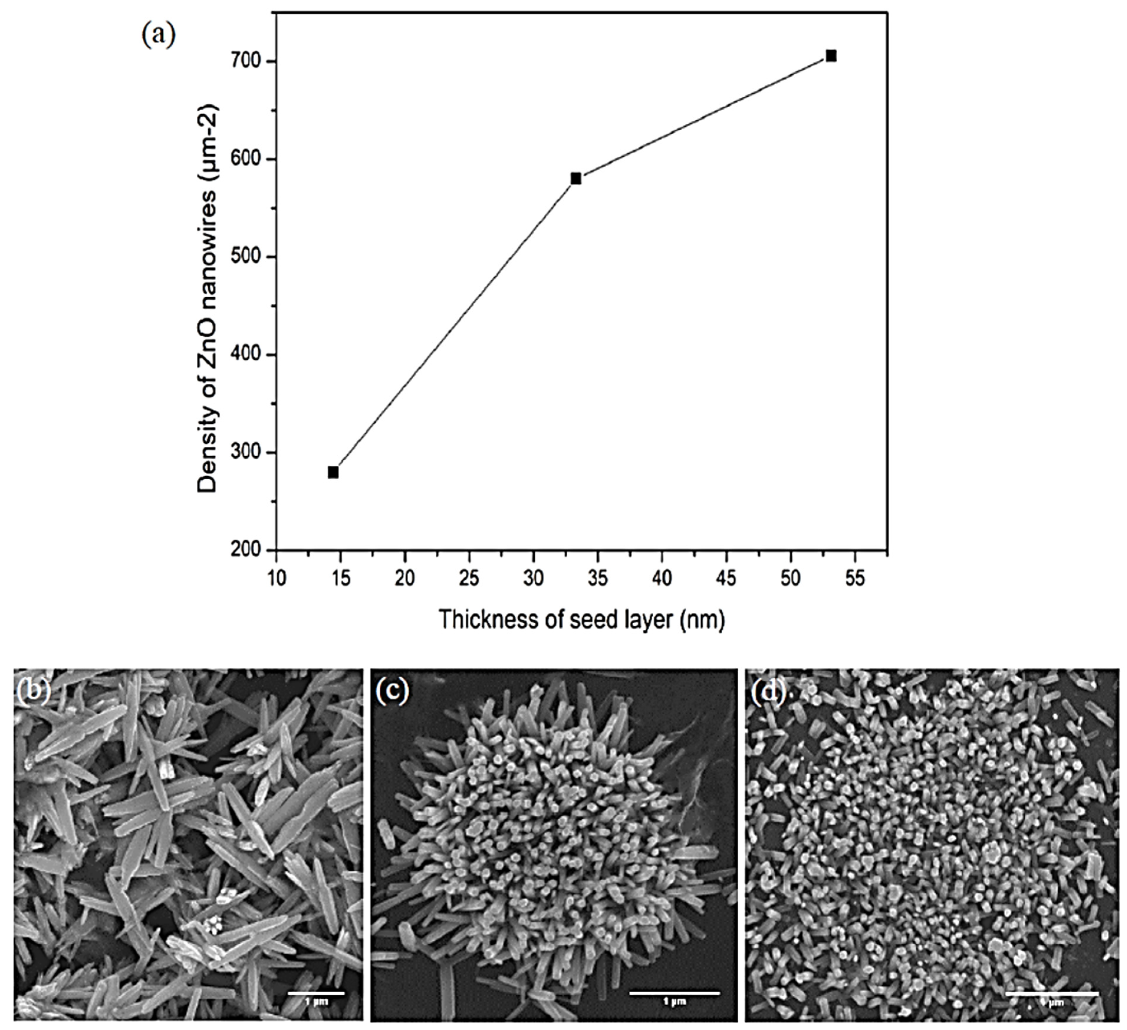
3.2. Morphology of ZnO Nanowires

Figure 2 shows FESEM images of various seed layer thicknesses. Figure 2 shows that the ZnO nanowires in the one-layer sample have a flower-like structure, whereas the ZnO nanowires in the three-layer and five-layer samples have a rod-like structure. This result can be explained by the seed layer condition relationship. It is possible to categorize this work as having two processes. The first is the deposition of a seed layer during the sol–gel spin coating method, and the second is the growth of ZnO nanowires in the CBD solution. It should be noted that the seed layer’s condition is important for the growth of ZnO nanowires. During the first seed layer deposition process, the one-layer sample with the smallest seed layer thickness has a smaller seeding area and thus provides a smaller growth area for ZnO nanowires, whereas the maximum seed layer thickness of a five-layer sample has a larger growth area for nanowires. Later, during CBD, the ZnO particles from the solution are attached to the seed layer provided by the first process for the growth of nanowires. However, the initial process’s space limitation allowed for an excess of ZnO particles. The excess ZnO particles then adhered to the tips of the ZnO nanowires formed from the seed layer. The first reason for ZnO particle attachment to other ZnO nanowires is due to its polar side. ZnO nanorods have polar sides that are Zn-terminated at the top and OH-terminated at the bottom. This quasistable polar side can attract opposite charges (Zn2+ and OH−) from the solution to form nuclei [23]. The second reason is due to defects (Figure 2a) at the tips of the nanowires. These defects have higher surface energy, making them unstable. To reduce surface energy, ZnO particles attach to the polar side of ZnO nanowires grown from the seed layer, forming a stick-like structure known scientifically as an oriented attachment. Individual nanowires have relatively high surface energy due to the presence of two major exposed planes. As a result, they tend to aggregate to reduce surface energy by reducing the exposed area. In contrast, the rod-like structure of ZnO nanowires shown in Figure 2b,c is grown with hexagonal sidewalls of wurtzite structure (Figure 2b,c) and no defects at the nanowire tip. This structure is said to have achieved stable orientation [24].
Figure 3 depicts the average diameter and length of ZnO nanowires at various layers. The average diameter of ZnO nanowires increases linearly as the thickness of the ZnO seed layer increases from one layer to five layers. The length of the obtained ZnO nanowires, on the other hand, decreases as the seed layer thickness increases. Table 3 summarizes the diameter and length of ZnO nanowires obtained.
The diameter of the ZnO nanowires was found to be influenced by the crystallite size of the seed layer in this study. As previously stated, a one-layer sample has the smallest seed layer thickness, resulting in a smaller crystallite size. This will result in ZnO nanowires that are longer and smaller due to axial growth (vertical y-axis growth). Similarly, larger crystallite sizes result in shorter and larger ZnO nanowires, a process known as radial growth (horizontal x-axis growth). Table 2 shows that the results agree with the crystallite size. Song and Lim (2007) discovered a similar result using sputter deposition [13]. In their report, they discovered that thinner seed layers had smaller crystals and a larger surface area. As a result, for thin seed layers, the diameter of the nanowires is reduced. A thicker seed layer, on the other hand, has a larger crystal size and a smaller surface area, resulting in a larger ZnO nanowire diameter.

3.3. Density of ZnO Nanowires

The number of ZnO nanowires present per micron was used to calculate the density of ZnO nanowires. Figure 4 depicts an increasing trend of ZnO nanowire density with increasing seed layer thickness in this work. As the thickness of ZnO nanowires increases from 14.43 to 33.31 nm, the density increases rapidly. Later, the density in the five-layer sample increases significantly to the range of 650–700 μm−2. Furthermore, the increase in the density of ZnO nanowires with increasing seed layer thickness can be explained by the number of ZnO adatoms. As a result, the seed layer produces more ZnO nanowires. The seed layer thickness can control the diameter and density of ZnO nanowires [15]. To investigate the effect of seed layer thickness, nanowires were grown in a gas flow with varying film thickness. All samples show an increasing trend in the diameter of ZnO nanowires. According to Fang et al. (2007), the increasing number of ZnO nanowires is due to the fact that the minimal seed layer thickness is too thin to coat the entire substrate, resulting in some bare Si substrate [15]. It should be noted that nanowires cannot be grown on a Si substrate directly. It is possible to coat the entire substrate by increasing the seed layer thickness. A thicker seed layer can form larger seeds, resulting in the formation of more ZnO nanowires from the seed layer.

3.4. Alignment of ZnO Nanowires

These findings are completely consistent with the AFM images shown in Figure 5. Because of the nature of the silicon substrate, the seed layer has a rougher surface. Murillo et al. (2015) report that the silicon substrate is not as smooth as it appears to the naked eye [25]. The surface of the silicon substrate, on the other hand, is quite rough. As a result, as the number of layers increases, the surface becomes rougher. Many researchers have related the surface roughness with the vertically well-aligned ZnO nanowires. Theoretically, the rougher the surface, the better the alignment of ZnO nanowires. This is due to the rougher surface providing more mechanical interlocking at the interface [23]. As a result, stronger bonds are formed between the solute in the CBD solution and the surface of the seed layer.
Figure 6 shows that the surface roughness of the ZnO seed layer increases significantly from 0.45 to 1.30 nm as the seed layer thickness increases from 14.43 to 53.14 nm, respectively.
However, in our case, we can see that none of the three samples have vertically aligned ZnO nanowires. A flower-like structure can be seen in the one-layer sample of ZnO nanowires with a seed layer thickness of 14.43 nm. The three-layer and five-layer ZnO nanowire samples with seed layer thicknesses of 33.31 and 53.14 nm showed a slightly similar alignment. Some nanowires are not aligned, but rather grow in a specific orientation. As a result, we observed numerous directional ZnO nanowires growing from planes (100), (002), (101), (102), (110), and (103). Hu et al. (2010) proposed a schematic diagram illustrating the growth orientation of ZnO nanowires (Figure 7). Figure 7a clearly shows that ZnO nanowires grow in a vertical c-axis orientation perpendicular to the substrate with preferential (002) planes. On the other hand, the ZnO nanowires of (101) planes grow with a pyramid-like structure along the c-axis parallel to the substrate (Figure 7b). Similarly, for a polygon structure, ZnO nanowires of (100) planes grow in the c-axis parallel to the substrate (Figure 7c). In general, we can conclude that the alignment of ZnO nanowires is affected not only by surface roughness but also by nanowire growth orientation [26].

4. Conclusions

In this study, a ZnO seed layer was deposited and experiments were performed using the sol-gel spin coating technique to determine the role of seed layer thickness in the growth of ZnO nanowires. After that, the ZnO thin film was dipped in the CBD solution for 3 h in a conventional oven to grow the ZnO nanowires. A thinner seed layer results in a smaller crystal size, a smaller seeding area, and a smoother surface. As a result, ZnO nanowires grow in response to the seed layer condition. According to the XRD analysis, increasing the seed layer thickness improves crystallinity, and preferential growth occurs at the (101) planes. The increasing size of the crystallites indicates the function of layer coatings. This finding indicates that the length and diameter of ZnO nanowires are affected by the size of the crystallites. A thinner seed layer allows for smaller crystallite sizes, resulting in longer and thinner nanowires. Similarly, the thicker seed layer formed shorter and thicker nanowires with larger crystallite sizes. Furthermore, the density of ZnO nanowires is proportional to the number of ZnO adatoms. The density of ZnO nanowires increases as the number of ZnO adatoms increases. According to this relationship, the five-layer sample has a higher density of ZnO nanowires (668 µm−2), while the one-layer sample has the lowest density of ZnO nanowires. The ZnO nanowires grown in the thinner seed layer of the one-layer sample, on the other hand, have a flower-like structure, whereas the thicker seed layer three-layer and five-layer samples have a rod-like structure. The hexagonal shape rod of nanowires grown in a rod-like structure was discovered, indicating the wurtzite structure of ZnO nanowires. ZnO nanowires were dispersed between the patterned metal electrodes or sandwiched between them. In general, devices using a multitude of nanowires offer high signals due to the availability of a large sensing area. Usually, they require a fine-tuning of the synthetic approach and deposition processes in multiple steps that may include growth, sonication, and distribution of the nanowires on the prepatterned electrodes.

Author Contributions

Conceptualization, Z.H.A. and S.P.; Data curation, S.N.M.A., S.A., S.S. and R.S.; Formal analysis, Z.H.A., S.A., R.S. and S.P.; Funding acquisition, S.P.; Investigation, S.N.M.A. and S.P.; Methodology, Z.H.A. and S.P.; Validation, S.N.M.A., S.A., S.S. and R.S.; Visualization, S.N.M.A., S.A., S.S. and R.S.; Writing—original draft, Z.H.A. and S.P.; Writing—review & editing, S.S. All authors have read and agreed to the published version of the manuscript.

Funding

The authors gratefully acknowledge the support from Universiti Putra Malaysia research grants 9457700 and 9456800. We would also like to extend our appreciation to the Ministry of Education Malaysia (under the Fundamental Research Grant Scheme (FRGS) FRGS/1/2017/STG07/UPM/02/10, FRGS/2/2013/ST05/UPM/02/3, and the Exploratory Research Grant Scheme (ERGS) 5527188) for providing financial support.

Institutional Review Board Statement

Not applicable.

Informed Consent Statement

Not applicable.

Data Availability Statement

Not applicable.

Conflicts of Interest

The authors declare no conflict of interest with this work.

References

  1. Paiman, S.; Ling, T.H.; Husham, M.; Sagadevan, S. Significant effect on annealing temperature and enhancement on structural, optical and electrical properties of zinc oxide nanowires. Results Phys. 2020, 17, 103185. [Google Scholar] [CrossRef]
  2. Lausecker, C.; Salem, B.; Baillin, X.; Roussel, H.; Sarigiannidou, E.; Bassani, F.; Appert, E.; Labau, S.; Consonni, V. Formation mechanisms of ZnO nanowires on polycrystalline Au seed layers for piezoelectric applications. Nanotechnology 2019, 30, 345601. [Google Scholar] [CrossRef] [PubMed] [Green Version]
  3. Mustaffa, S.N.A.; Ariffin, N.A.; Khalaf, A.L.; Yaacob, M.H.; Tamchek, N.; Paiman, S.; Sagadevan, S. Sensing mechanism of an optimized room temperature optical hydrogen gas sensor made of zinc oxide thin films. J. Mater. Res. Technol. 2020, 9, 10624–10634. [Google Scholar] [CrossRef]
  4. Abubakar, S.; Khalid, N.; Rahman, S.F.A.; Tee, T.S.; Hamidon, M.N.; Talib, Z.A.; Sagadevan, S.; Paiman, S. Fabrication and characterization of nanostructured zinc oxide on printed microcontact electrode for piezoelectric applications. J. Mater. Res. Technol. 2020, 9, 15952–15961. [Google Scholar] [CrossRef]
  5. Ghazali, M.N.I.; Izmi, M.A.; Mustaffa, S.N.A.; Abubakar, S.; Husham, M.; Sagadevan, S.; Paiman, S. A comparative approach on One-Dimensional ZnO nanowires for morphological and structural properties. J. Cryst. Growth 2021, 558, 125997. [Google Scholar] [CrossRef]
  6. Kulkarni, S.S.; Mahavidyalaya, S.S.; Shirsat, M.D. Optical and Structural Properties of Zinc Oxide Nanoparticles. Int. J. Adv. Res. Phys. Sci 2015, 2, 14–18. [Google Scholar]
  7. Lee, C.T. Fabrication methods and luminescent properties of ZnO materials for light-emitting diodes. Materials 2010, 3, 2218–2259. [Google Scholar] [CrossRef] [Green Version]
  8. Fulati, A. Mechanical Characterization and Electrochemical Sensor Applications of Zinc Oxide Nanostructures; Linköping University Electronic Press: Linköping, Sweden, 2010; p. 61. [Google Scholar]
  9. Li, C.; Li, X.; Wang, D. Fabrication of ZnO Thin Film and Nanostructures for Optoelectronic Device Applications. In Oxide Thin Films, Multilayers, and Nanocomposites; Mele, P., Endo, T., Arisawa, S., Li, C., Tsuchiya, T., Eds.; Springer: Berlin/Heidelberg, Germany, 2015; pp. 239–271. [Google Scholar]
  10. Bhunia, S.; Palit, M.; Das, A.; Chattopadhyay, S.; Paul, S.; Karmakar, A. Investigation of The Properties of Single-step and Double-step Grown ZnO Nanowires Using Chemical Bath Deposition Technique. Adv. Mater. Lett. 2016, 7, 610–615. [Google Scholar]
  11. Park, D.J.; Kim, D.C.; Lee, J.Y.; Cho, H.K. Synthesis and microstructural characterization of growth direction controlled ZnO nanorods using a buffer layer. Nanotechnology 2006, 17, 5238. [Google Scholar] [CrossRef]
  12. Kim, D.C.; Kong, B.H.; Cho, H.K.; Park, D.J.; Lee, J.Y. Effects of buffer layer thickness on growth and properties of ZnO nanorods grown by metalorganic chemical vapour deposition. Nanotechnology 2007, 18, 015603. [Google Scholar] [CrossRef]
  13. Song, J.; Lim, S. Effect of seed layer on the growth of ZnO nanorods. J. Phys. Chem. C 2007, 111, 596–600. [Google Scholar] [CrossRef]
  14. Zhao, D.X.; Andreazza, C.; Andreazza, P.; Ma, J.; Liu, Y.; Shen, D. Buffer layer effect on ZnO nanorods growth alignment. Chem. Phys. Lett. 2005, 408, 335–338. [Google Scholar] [CrossRef]
  15. Fang, F.; Zhao, D.X.; Zhang, J.Y.; Shen, D.Z.; Lu, Y.M.; Fan, X.W. Growth of well-aligned ZnO nanowire arrays on Si substrate. Nanotechnology 2007, 18, 235604. [Google Scholar] [CrossRef]
  16. Wu, W.Y.; Yeh, C.C.; Ting, J.M. Effects of seed layer characteristics on the synthesis of ZnO nanowires. J. Am. Ceram. Soc. 2009, 92, 2718–2723. [Google Scholar] [CrossRef]
  17. Yin, Y.T.; Que, W.X.; Kam, C.H. ZnO nanorods on ZnO seed layer derived by sol-gel process. J. Sol.-Gel. Sci. Technol. 2010, 53, 605–612. [Google Scholar] [CrossRef]
  18. Peiris, T.A.N.; Alessa, H. Effect of ZnO seed layer thickness on hierarchical ZnO nanorod growth on flexible substrates for application in dye-sensitised solar cells. J. Nanoparticle Res. 2013, 15, 2115. [Google Scholar] [CrossRef]
  19. Ji, L.; Peng, S.; Wu, J.; Shih, W.; Wu, C.; Tang, I. Journal of Physics and Chemistry of Solids Effect of seed layer on the growth of well-aligned ZnO nanowires. J. Phys. Chem. Solids 2009, 70, 1359–1362. [Google Scholar] [CrossRef]
  20. Wallace, I.; Eshu, O.V.; Chukwunonso, O.B.; Okoro, U.C. Synthesis and characterization of zinc oxide (ZnO) nanowire. J. Nanomed. Nanotechnol. 2015, 6, 1000321. [Google Scholar]
  21. Khan, M.I.; Bhatti, K.A.; Qindeel, R.; Alonizan, N.; Althobaiti, H.S. Characterizations of multilayer ZnO thin films deposited by sol-gel spin coating technique. Results Phys. 2017, 7, 651–655. [Google Scholar] [CrossRef]
  22. Zheng, Y.; Vassiljev, N.; Konstantinidis, A.; Griffiths, J.; Speller, R. Limit of Detection in X-ray Diffraction Measurements of Tissue Equivalent Samples. J. Phys. Conf. Ser. 2015, 637, 012037. [Google Scholar] [CrossRef] [Green Version]
  23. Ghayour, H.; Rezaie, H.R.; Mirdamadi, S.; Nourbakhsh, A.A. The effect of seed layer thickness on alignment and morphology of ZnO nanorods. Vacuum 2011, 86, 101–105. [Google Scholar] [CrossRef]
  24. Qiu, J.; Weng, B.; Zhao, L.; Chang, C.; Shi, Z.; Li, X.; Hwang, Y.H. Synthesis and characterization of flower-like bundles of ZnO nanosheets by a surfactant-free hydrothermal process. J. Nanomater. 2014, 2014, 281461. [Google Scholar] [CrossRef] [Green Version]
  25. Murillo, G.A.C.; Bojorge, C.D.; Heredia, E.A.; de Reca, N.E.W. Study of the Substrate Influence in ZnO Nanowires Oriented Growth. Procedia Mater. Sci. 2015, 8, 630–634. [Google Scholar] [CrossRef] [Green Version]
  26. Hu, Y.H.; Chen, Y.C.; Xu, H.J.; Gao, H.; Jiang, W.H.; Hu, F.; Wang, Y.X. Texture ZnO thin-films and their application as front electrode in solar cells. Engineering 2010, 2, 973–978. [Google Scholar] [CrossRef] [Green Version]
Figure 1. XRD results of the (a) ZnO seed layer (b) ZnO nanowires of different seed layer thickness.
Coatings 12 00474 g001
Figure 2. FESEM images of the ZnO nanowires grown on ZnO seed layer thickness of (a) one-layer sample, (b) three-layer sample, and (c) five-layer sample.
Coatings 12 00474 g002
Figure 3. The length and diameter of ZnO nanowires grown.
Coatings 12 00474 g003
Figure 4. Graph of (a) density of ZnO nanowires with different seed layer thickness according to FESEM images of (b) one-layer sample, (c) three-layer sample, and (d) five-layer sample.
Coatings 12 00474 g004
Figure 5. AFM images of ZnO seed layer on different thicknesses: (a,b) one-layer sample; (d,e) three-layer sample; (g,h) five-layer sample. FESEM cross-section view (c,f,i) images of ZnO nanowires.
Coatings 12 00474 g005
Figure 6. Surface roughness of seed layer measured with corresponding seed layer thickness.
Coatings 12 00474 g006
Figure 7. Schematic diagram of the relationship between microstructure and crystal growth orientation of ZnO: (a) a columned structure of c-axis growth perpendicular to the substrate, (b) a pyramid-like structure of c-axis growth parallel to the substrate, and (c) polygon structure of c-axis growth parallel to the substrate [26].
Coatings 12 00474 g007
Table 1. Features of multilayer ZnO thin film deposited by a sol-gel spin coating technique.
Name of SampleNumber of LayersThickness of ZnO Seed Layer (nm)
1 layer114.43 ± 1.46
3 layer333.31 ± 11.31
5 layer553.14 ± 9.01
Table 2. Characteristic of ZnO seed layer of (101) plane estimated from XRD patterns.
Name of SampleFWHM (°)Crystallite Size (nm)
1 layer0.5431.85
3 layers0.4736.59
5 layers0.2959.38
Table 3. Summary of the length and diameter of ZnO nanowires.
Name of SampleLength of ZnO Nanowires (nm)Diameter of ZnO
Nanowires
1 layer870.29 ± 54.7640.73 ± 1.52
3 layers422.51 ± 32.7364.17 ± 6.27
5 layers193.05 ± 9.1384.80 ± 3.86
Publisher’s Note: MDPI stays neutral with regard to jurisdictional claims in published maps and institutional affiliations.

