Article

Effect of Electromigration and Thermal Ageing on the Tin Whiskers’ Formation in Thin Sn–0.7Cu–0.05Ga Lead (Pb)-Free Solder Joints

by
Noor Zaimah Mohd Mokhtar
1,2,
Mohd Arif Anuar Mohd Salleh
1,2,*,
Andrei Victor Sandu
1,3,4,5,
Muhammad Mahyiddin Ramli
1,6,
Jitrin Chaiprapa
7,
Petrica Vizureanu
1,3,* and
Mohd Izrul Izwan Ramli
1,2
1
Centre of Excellence Geopolymer & Green Technology (CEGeoGTech), Universiti Malaysia Perlis (UniMAP), Arau 02600, Perlis, Malaysia
2
Faculty of Chemical Engineering Technology, Universiti Malaysia Perlis (UniMAP), Arau 02600, Perlis, Malaysia
3
Faculty of Materials Science and Engineering, Gheorghe Asachi Technical University of Iasi, D. Mangeron 41, 700050 Iasi, Romania
4
Romanian Inventors Forum, St. P. Movila 3, 700089 Iasi, Romania
5
National Institute for Research and Development in Environmental Protection, Splaiul Independenței 294, 060031 București, Romania
6
Faculty of Electronic Engineering Technology (FETech), Universiti Malaysia Perlis (UniMAP), Padang Besar 02100, Perlis, Malaysia
7
Synchrotron Light Research Institute (SLRI), Muang District, Nakhon Ratchasima 30000, Thailand
*
Authors to whom correspondence should be addressed.
Coatings 2021, 11(8), 935; https://doi.org/10.3390/coatings11080935
Submission received: 30 June 2021 / Revised: 20 July 2021 / Accepted: 30 July 2021 / Published: 4 August 2021
(This article belongs to the Special Issue Surface Treatment of Metals)

Abstract

:
The investigation on tin (Sn) whiskers formation has been widely applied in the field of lead-free electronic packaging. This is due to the fact that use of the Sn–Pb finishes has converted to Pb-free finishes in the electronic industry. Sn whiskers can grow long enough to cause a short circuit, which affects electronic devices’ reliability. This study investigates Sn whiskers’ formation in the thin Sn–0.7Cu–0.05Ga Pb-free solder under the influence of electromigration and thermal ageing for surface finish applications. The samples were stored in ambient conditions for 1000 h before being exposed to electromigration and thermal ageing to study the corresponding whiskers’ growth. A scanning electron microscope (SEM) was used to study the Sn whiskers’ microstructure, while an optical microscope (OM) was utilized to investigate the IMC layers in the samples. The results show that the addition of 0.05 wt.% gallium (Ga) decreased the Sn whisker’s length and growth density while simultaneously refining the IMC layers. Synchrotron micro-XRF (µ-XRF) shows the existence and distribution of Ga addition in both electromigration and thermal ageing samples. The shear test was used to determine the solder alloys’ mechanical properties. As a result, the addition of Ga to the Sn–0.7Cu solder improved the fracture morphology of solder joints. In conclusion, Ga’s addition resulted in decreasing Sn whisker formation and refining of the IMCs while also increasing the shear strength of the Sn–0.7Cu solder by ~14%.

1. Introduction

The rapid advancement of electronic packaging has tremendously improved the performance of its related products and services. Electronic interconnects play a crucial role in advanced electronic packaging systems as it links and provides mechanical support to the integrated circuits (ICs) and printed circuit boards (PCBs). This impacts the reliability and longevity of electronic devices. Eutectic tin–lead (Sn–Pb) solder is used to attach discrete components to PCBs. In fact, Pb provides ductility to the Sn–Pb solder. Alloying Pb with Sn significantly improves the Sn-base solder’s mechanical properties, as it suppresses whiskers’ formation [1,2,3,4]. However, Pb is toxic to humans and the environment, which necessitates the introduction and the usage of Pb-free solders [5,6].
Several types of Sn-based Pb-free solders, such as Sn–Ag, Sn–Cu, Sn–Zn, Sn–Bi, Sn–In, and Sn–Ag–Cu have been developed to replace the conventional Sn–Pb solder alloys [7,8,9]. In response to this, Sn–Cu lead-free solder has attracted wide attention because of its excellent and comprehensive performance, low cost, and widespread use in electronic packaging. Therefore, Pb-free solder with high concentrations of Sn was chosen by manufacturers to replace Sn–Pb solder [10,11]. According to several studies, the adoption of high-Sn content, Pb-free solders has also created an issue related to Sn whisker formation, which is creating another reliability concern [12,13]. Sn whiskers, needle-shaped single crystals measuring hundreds of microns long and several microns wide, sometimes trigger current shortages and other failures in electronics.
Furthermore, at room temperature, Sn whiskers can grow spontaneously. A tin whisker is known to grow up to a length of several millimeters (mm), and occasionally to lengths of 10 mm. Short circuits caused by tin whiskers have caused numerous electronic system failures after connecting electrically contrasting elements. When solder containing Sn wets copper (Cu) substrate, stress is initially created. The stress is affected by the interaction between the coating and the metal substrate [14,15]. In this case, the Cu atoms diffuse into the Sn. The Cu atoms also react with Sn atoms to form intermetallic compounds such as Cu6Sn5, which distort the Sn coating and build up compressive stress within the Sn, which encourages whisker formation [16]. Excessively, thick interfacial IMC may create stress concentration, and hence initiates cracks which may aggravate the Sn area and, eventually, the surface of Sn coating. In addition, whisker growth also involves atoms diffusing into the whisker from the area surrounding its base [17].
The term electromigration refers to the displacement of metal atoms in conductors. It is a diffusion process of solids driven by electric current [18]. In order to manifest this phenomenon, the current density must be sufficient to cause a drift in the direction of the electron flow. This can cause the initial microvoids in the conductor at high current densities (from where the material is transported), and hillock formations on the other side of the structure (where the material is deposited) [19]. The current stressing causes the diffusion of Sn towards cathode [20]. The IMC formed from Sn’s and Cu’s reaction breaks the Sn’s surface oxide, resulting in compressive stress in the Sn. Whenever an oxide layer is broken at a weak spot, it exposes a stress-free surface that creates a compressive stress gradient, which is relaxed by growing whiskers [21]. Fukuda et al. investigated the whisker growth of bright and matte Sn-plated Cu for an eight-month assessment under electrical current. He reported that whiskers’ growth on both the cathode and anode increased the standard deviation of the length distribution and generated longer whiskers [22]. Lin et al. revealed that the electric current’s stress produced more whiskers, especially at higher current density [23].
Stress generation can also be increased with thermal ageing. Higher temperatures and humidity promote whisker growth through oxidation and corrosion. The diffusion of atoms causes stress to accumulate during the ageing process, and its accumulation further accelerates the diffusion reaction. Lin et al. studied flip-chip solder joints to determine how temperature affects electromigration, and found that as the temperature increased, electromigration became significantly worse. This is because the diffusion of the Cu atom is increased with increasing temperature, causing movement rate to also increase [24].
Sn solders are being improved in various ways to increase their reliability and properties and reduce the whiskers formation. One useful approach is to add ternary constituent to increase its performance. For example, Ga has many desirable physical properties such as low melting point (29.78 °C), as well as being both electrically and thermally conductive [25]. Moreover, Ga can wet most metals and oxides without requiring flux, which makes it a very attractive material for Sn–Cu solder.
This study investigates the effect of electromigration with and without thermal ageing on the growth of Sn whiskers on the surface of Sn–0.7Cu alloys. The accelerated tests were used to induce whiskers to study the diffusion and stress behavior. We also investigated the effect of Ga addition on the growth of Sn whiskers. Furthermore, we analyzed, using synchrotron micro-XRF, shear strength, and microhardness of Sn–0.7Cu–0.05Ga, how Ga affected the properties of Sn–0.7Cu solders and whiskers formation. The electromigration and thermal ageing effect processes were used to accelerate stress behavior.

2. Materials and Methods

2.1. Materials Preparation

The Sn–0.7Cu solder was supplied by Nihon Superior (M) SDN. BHD. (Perak, Malaysia). The base materials consist of 99.3 wt.% Sn and 0.7 wt.% Cu, while Sn–0.7Cu–0.05Ga consists of 0.05 wt.% Ga addition. The raw materials were melted in a graphite crucible in a furnace at 350 °C and held for 1 h in a vacuum condition. An amount of 0.05% Ga was added to the melt and stirred every 15 min to homogenize the solder alloy. The solder alloy was then cast into ingots.

2.2. Dipping for Solder Coating

An automated dipping machine by Nihon Laboratory UniMAP (Osaka, Japan) was used to perform a solder coating. A Cu sheet substrate, which was 99.9% pure, was first cleaned using acid cleaning liquid that contains 5 g (35%) of hydrochloric acid with 95 g of deionized water (1.75%) for 3 min to remove surface oxides and contaminations. Then, the Cu sheet was rinsed with acetone and distilled water to remove possible surface contamination, and quickly dried in the air. After that, it was dipped into the flux for 3 s before being fixed on one side straight up from the liquid-heated molten solder for 3 s to generate surface finishes. The temperature of the solder bath was 300 °C during dipping. After the dip soldering, the soldered samples were cleaned with acetone and ultrasonic cleaner. Each sample was subsequently used in four test conditions: as received, after electromigration, after storage at a temperature of 60 °C, and 120 °C. After that, the entire sample was deep-etched to remove the solder and reveal the IMC grains. The deep-etch solution consists of 93% of distilled water, 5% hydroxide, and 2% of ortho-nitrophenol.

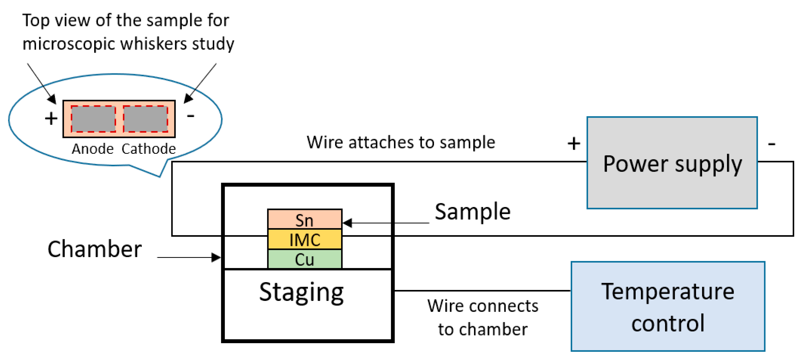
2.3. Whiskers Accelerated Test by Electromigration Testing and Electromigration with Thermal Ageing

There were two tests were carried out. The first set of samples was subjected to electromigration testing conditions. The testing was carried out in room temperature. The sample was connected with the current stressing at a current density of 1 × 10³ A/cm2 at room temperature, while the second set of samples was the electromigration with the thermal ageing test at temperature of 60 °C and 120 °C. The schematic diagram of the electromigration with the thermal ageing test is shown in Figure 1. The sets of samples were divided into two, one which was for whiskers observation, the other one for IMC observation. For IMC observation, the samples were mounted on the cross section with a combination of resin and hardener. Then, it was ground and polished to reveal the IMC thickness’ layer. The electromigration, with and without thermal ageing, on the Sn whisker growth and IMCs were then determined. The current density was calculated using Equation (1). For the observation of solder microstructures, all cast samples were carefully polished with sandpapers and diamond paste to remove surface scratches, washed with CH3OH, and dried. Optical microscopy was conducted to confirm the microstructural characterizations.
J = C u r r e n t   ( A ) A r e a   ( cm 2 )

2.4. Tin Whiskers Analysis and Characterization

Java image processing program known as ImageJ (LOCI, University of Wisconsin, Madison, WI, USA) was used to measure the thickness of the interfacial IMCs formed at the solder/Cu [26,27]. The IMC thickness is equal to the IMC area divided by the length of the IMC, as per Equation (2) and Figure 2. Measurements of three samples of each type on different areas of images were conducted. The total length of each images measured was in the range of ~150 µm.
I M C   T h i c k n e s s = A r e a   o f   I M C L e n g t h   o f   I M C
The morphology of the Sn whiskers formed on the surface of the samples was imaged. A Joint Electron Device Engineering Council (JEDEC) Whisker Standard (JESD22-A121A) was used to measure the Sn whiskers’ length and density. The samples’ surface morphology was characterized using an optical microscope (OM) and scanning electron microscope (SEM) JEOL-JSM6460 LA by JEOL Ltd. (Tokyo, Japan). Two methods can measure the Sn whiskers’ dimensions: the radial method and the axial method. The radial method is used to measure the straight-line distance from the emergence point of Sn whiskers to the apex point of the whiskers, while the axial method measures the distance from the surface of the Sn layer to the apex point of the whiskers formed if the whiskers are vertical to the surface. This research utilized the radial method to measure the whiskers’ length. The test conditions are summarized in Table 1.
The elemental distribution analysis of the solder alloy was conducted using synchrotron micro-X-ray fluorescence (µ-XRF) at the Synchrotron Light Research Institute (SLRI, Nakhon Ratchasima, Thailand). Testing was performed in BL6b beamline using continuous synchrotron radiation from a bending magnet of the 1.2 GeV electron storage ring. Micro-X-ray beams with size of 30 µm × 30 µm were initiated on the samples using the polycapillary lens and then focused with the continuous synchrotron radiation with the range energy of 2–12 keV. The cross-section sample was initially mounted with a mixture of hardener and resin, and carefully grounded to 2 mm of thickness and mounted on a high-precision motorized stage. The fluorescence signal produced from the experiment was collected by the detector where the distance from the detector to the sample is in the range of 5–10 cm. Elemental spectrums and mappings were analyzed using PyMca 5.6.5- win64.exe software (European Synchrotron Radiation Facility, Grenoble, France).

3. Results

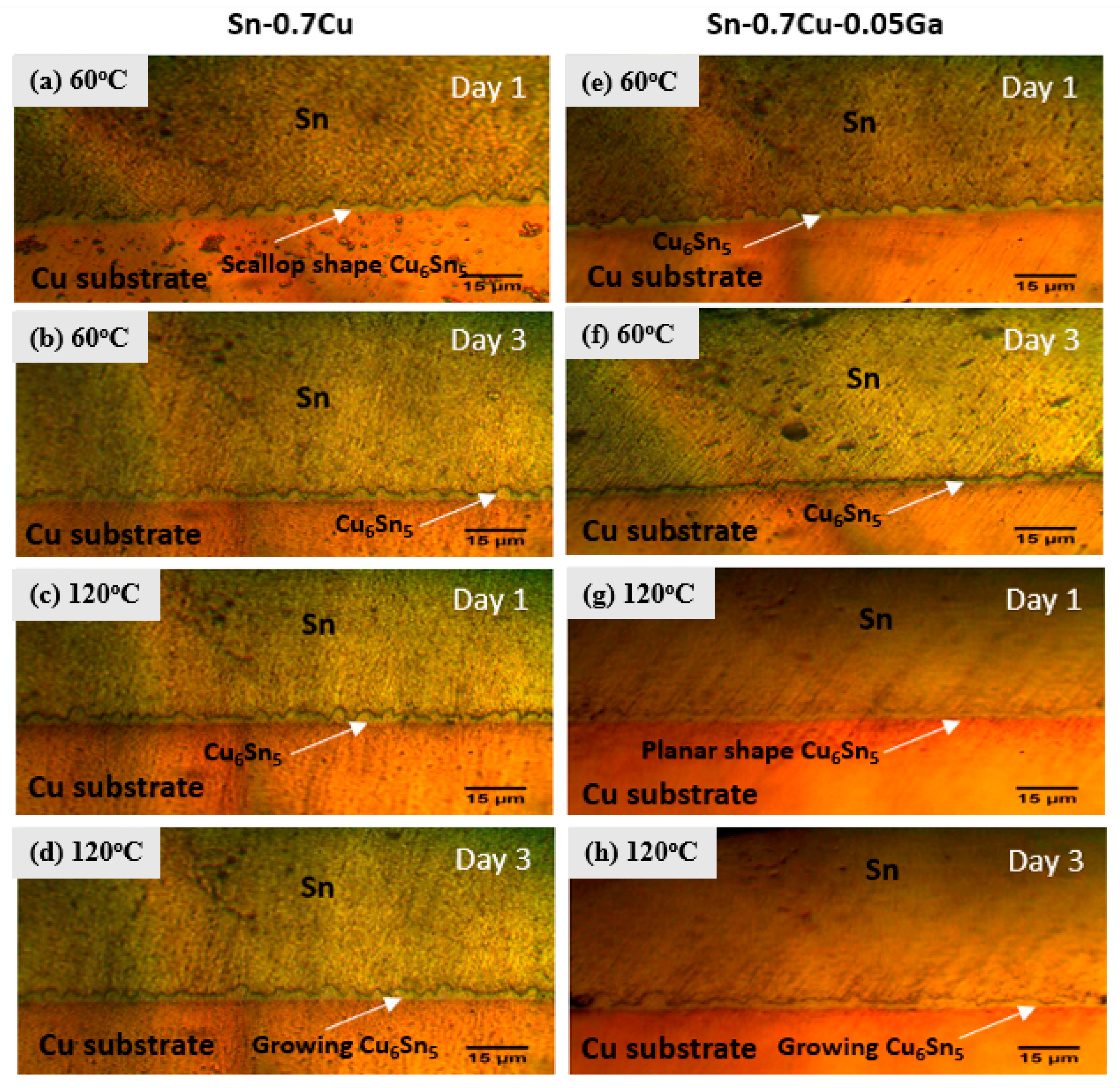
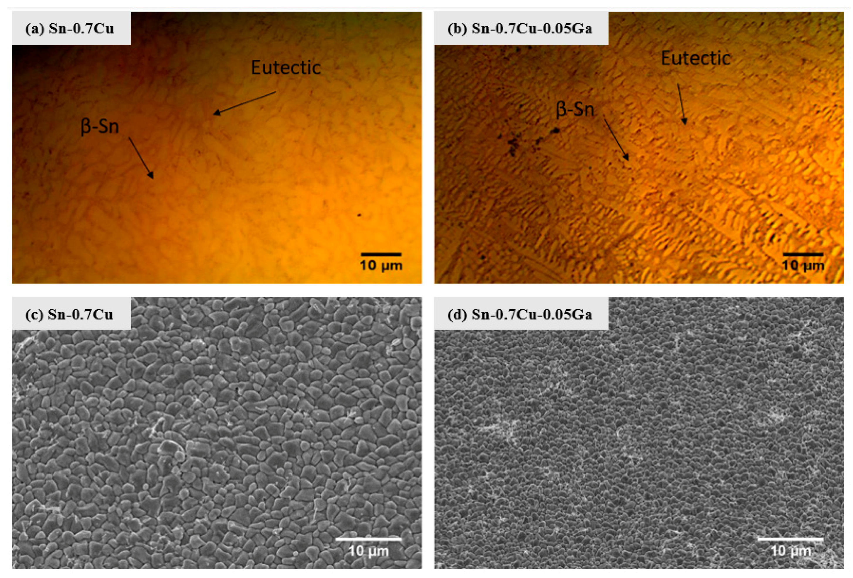
3.1. Microstructure Analysis

Figure 3 shows the typical micrograph captured by Olympus BX41RF Optical Microscope OM (Tokyo, Japan), on the soldered condition of the bulk microstructure and grain structure of the eutectic Sn–0.7Cu Sn–0.7Cu–0.05Ga solder alloy. The Sn–0.7Cu base alloy has a microstructure composed primarily of β–Sn matrix and eutectic phases, which is typical for Sn–0.7Cu eutectic solders (shown in Figure 3a,b). Although Sn–0.7Cu is near to the eutectic alloy, there are primary β–Sn dendrites in the microstructure. With the addition of 0.05 wt.% Ga, the microstructure of Sn–0.7Cu solder alloy became more refined where more dendritic crystals of β–Sn were formed. During the solidification process, Ga tends to adsorb on the surfaces of crystal planes, as well as the grain boundaries, which acts as a solid solution strengthening [25]. Two major reasons can be attributed to adsorption theory. Firstly, adsorption of Ga lowers the surface energy difference between crystal surfaces. Secondly, due to the pinning effect, the growth rate of the Ga-absorbing crystal surface is reduced, so the grains become smaller and more evenly distributed. Bulk microstructure of the Sn–0.7Cu–0.05Ga affected the morphology and size of the IMCs. Furthermore, Ga’s addition decreased the crystals’ surface energy and allowed smaller grain sizes to exist. This high level of adsorption reduces the free energy in the entire interface as well as the energy differences between crystal planes. In this way, crystals can be prevented from growing, and microstructures can be refined and uniform. As a result, the eutectic phases and β–Sn grains in the solder composed of Sn–0.7Cu–0.05Ga are much finer, and the whole microstructure is more homogeneous than that of the base alloy. Additionally, according to the Hall–Petch relationship, the optimized microstructure can improve the mechanical properties [28]. Figure 3c,d show the dipped solder of different samples that were stripped off selectively using an etching solution of 93% of distilled water, 5% hydroxide, and 2% of ortho-nitrophenol to investigate the evolution of the growth morphology of the intermetallic phase at the Sn/Cu interface. As shown in Figure 3c,d, the interfacial Cu6Sn5 grains are reduced with a Ga addition, while their morphologies remain ovoid.

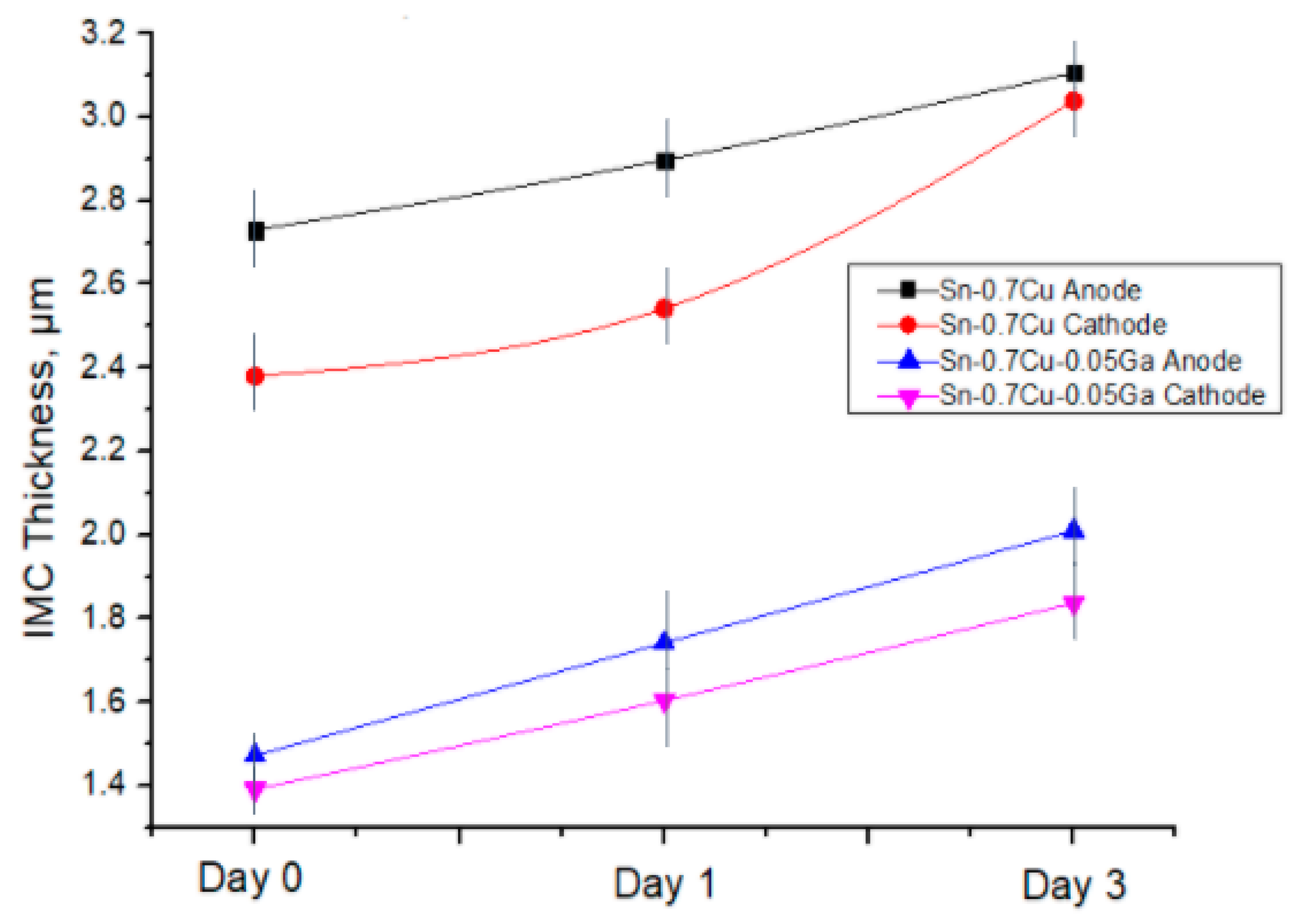
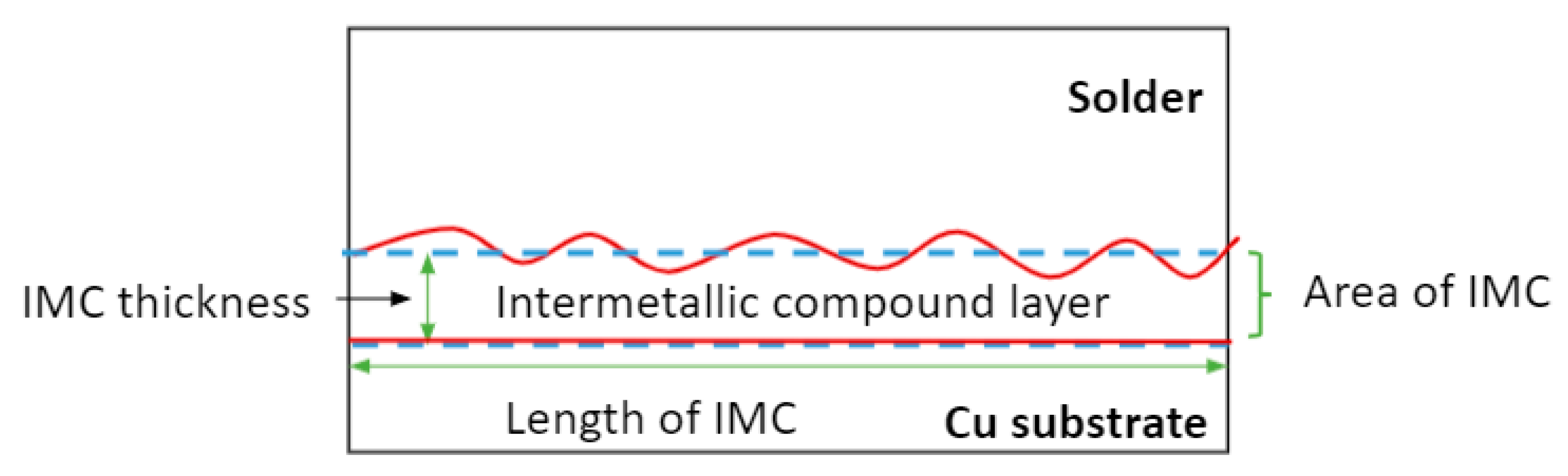
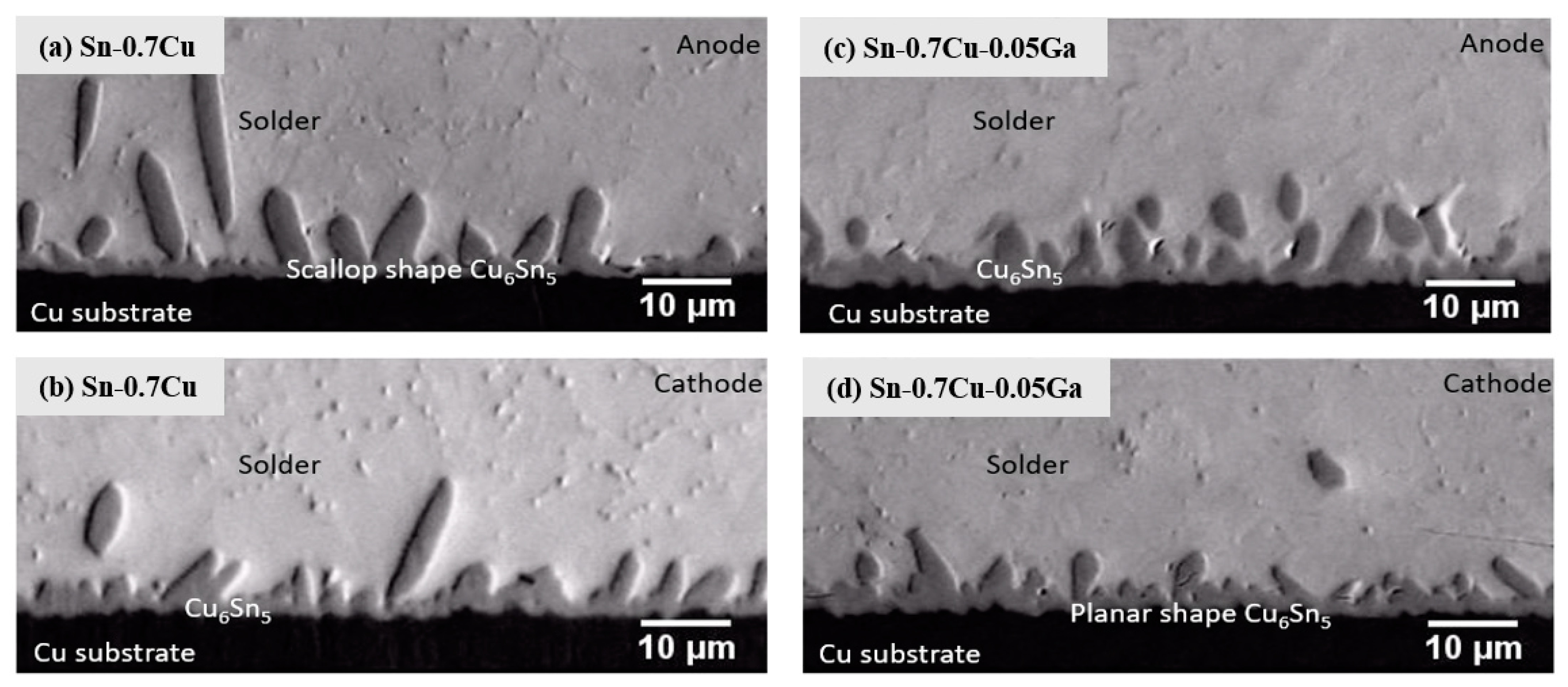
3.2. Interfacial Intermetallic Compound (IMC) during Electromigration

The growth of IMC in field service can affect the strength of solder joints and their mechanical failure. A layer of Cu6Sn5 IMC at the Cu substrate interface of Sn–0.7Cu and Sn–0.7Cu with 0.05 wt.% of Ga was observed on the anode and cathode sides. After current stressing at 30 °C in 3 days with current density of J = 1.0 × 10³ A/cm2, the IMC layer formed at the anode was thicker than the cathode (Figure 4 and Figure 5), which could be due to the electron migration from the cathode to anode side because of current flow. This quickens the IMC layer growth, thus creating thicker layers on the solder joints. Initially, the IMC layer of the Sn–0.7Cu solder joint has a thickness of 2.73 μm at the anode and 2.3 µm at the cathode, while the IMC layer of the Sn–0.7Cu–0.05Ga is 1.47 μm at the anode and 1.39 µm at the cathode, which is a decrease of 39% in the cathode and 46% at the anode. After 3 days, the thickness of the pure Sn–0.7Cu increased to 3.22 µm at the anode, while the thickness increased to 3.2 µm at the cathode. In the case of the Sn–0.7Cu–0.05Ga, the IMC thickness increased to 2.62 µm at the anode, while the IMC thickness at the cathode increased to 2.32 µm. The IMC layer for the Sn–0.7Cu–0.05Ga Pb-free solder grew more uniformly relative to that of the pure Sn–0.7Cu solder, recording a 27% decrease on the cathode and 18% decrease at the anode. Figure 5 presents the IMC thickness data for both the anode and the cathode for current stressing up to 3 days at 30 °C with current densities of J = 1.0 × 10³ A/cm2. In this case, the data before electromigration is also included as a reference. A parabolic dependence of IMC growth is found at the anode, as well as the absence of current. Compared with the no-current case, IMC grew faster at the anode side and slower at the cathode side. Thus, the polarity of the electric current resulted in enhanced growth of IMC at the anode and retarded growth at the cathode [20].
The interfacial IMC layer in the Sn–0.7Cu–0.05Ga appeared to be thin relative to that of the pure Sn–0.7Cu solder. In addition, Ga diffused slowly and prevented the IMC layer’s growth and secondary phases formation. The evident explanation for this behavior is that the Ga on the cathode area slows Cu diffusion into Sn by acting as a diffusion barrier [16,28]. The IMC tends to grow more slowly in samples that have no Ga added, as less Cu is able to diffuse through the interconnections. A thin, uniform, and continuous IMC layer is crucial towards forming excellent bonds. The solder joint becomes weak if it lacks any IMCs, due to the lack of interactions between the solders and substrates. On the other hand, thick IMC layers could degrade the solder joints’ reliability due to their brittle nature. The solid-solution strengthening of Ga altered the morphology growth positioning of the interfacial IMC [29]. As per these results, it can be seen that there is a refinement in the cathode’s IMC layer. The IMC thickness at the anode is higher than that of the cathode. During current stressing, the electric current flows from the cathode to the anode. The electrons move away from the cathode to the anode during current stressing, which increases the thickness of the IMC at the anode. The IMC’s growth occurs at the expense of the Cu substrate. Therefore, the supply of Cu increased the growth of the interfacial IMC at the anode. The stress gradient during electromigration is commonly known as “back stress” [30]. It was found that the anode underwent the highest compressive stress due to the accumulation of the atoms. The electromigration process pushes electrons towards the anode, which may create localized compressive stress. As a result of migration of electrons from the cathode side, moving atoms may create vacancies which may also appear as microvoids. In the absence of electric current, IMC grows according to the same parabolic rule as binary diffusion couples. High current density causes electromigration owing to momentum transfer from electrons to atoms with mass transfer in the same direction as electron movement. A similar result has also been shown in a study of whisker growth at a high current density with Sn stripes under complicated geometry [31].

3.3. Interfacial Intermetallic Compound (IMC) under Electromigration and Thermal Ageing

The electromigration effect and IMC formation at different ageing temperatures on the anode side were explored. Figure 6 shows optical micrograph of interfacial microstructure of aged samples at temperature of 60 °C and 120 °C. The image was captured at the anode side after ageing. A layer of Cu6Sn5 IMC layer was detected at the Cu substrate interface of Sn–0.7Cu and Sn–0.7Cu–0.05Ga solders. At the ageing temperature set up at 60 °C with constant current stressing of J = 1.0 × 10³ A/cm2 for 1 to 3 days, it was seen that the IMC layer thickness was considerably thicker compared to the IMC thickness at room temperature. The anode of the IMC thickness of Sn–0.7Cu and Sn–0.7Cu–0.05Ga solder under different condition and times are shown in Figure 6. In the pure Sn–0.7Cu Pb-free solder, the IMC thickness is 3.27 μm, while the IMC thickness of Sn–0.7Cu–0.05Ga Pb-free solder is 2.27 µm. When the ageing time was increased to 3 days, the IMC layer’s thickness grew to 3.29 µm for Sn–0.7Cu solder, while the thickness of the IMC layer increased to 2.36 µm for the Sn–0.7Cu–0.05Ga solder. The thickness of the interfacial IMC of Sn–0.7Cu–0.05Ga is thinner than that of the IMC of the pure Sn–Cu solder. It was a 0.6% increment for the Sn–0.7Cu and a 3.9% increment for the Sn–0.7Cu–0.05Ga solder. The IMC increment was considered significant.
From the figure, it can be seen the IMC grew faster at higher temperature. This is due to the fact that during ageing at higher temperature, the diffusion rate of Cu atoms is increased drastically [24]. Furthermore, the grooves and valleys between the interfacial IMC grains give an effect in terms of producing a convenient channel for Cu to pass through the previous IMCs and react with solder matrix to form more IMC grains. Then, in priority, the IMC layer thickens in the grooves. This leads to the transformation from scallop-like IMC layer to plate-like IMC layer [32].
When the ageing temperature was increased to 120 °C with constant current stress, the IMC’s thickness increased. The IMC of the pure Sn–0.7Cu solder on anode was 3.59 µm while the IMC thickness of Sn–0.7Cu–0.05Ga was 2.38 µm. When the heating time was increased to 3 days, the IMC layer thickness of both the pure Sn–0.7Cu and Sn–0.7Cu–0.05Ga Pb-free solder increased to 3.74 µm and 2.46 µm, respectively. The Sn–0.7Cu recorded an increase of 4.2%, while the Sn–0.7Cu–0.05Ga solder recorded an increase of 3.36%. Figure 7 presents the growth of IMC at higher temperature with the same current density of J = 1.0 × 10³ A/cm2. It also can be observed that the thickness of interfacial IMCs for all Sn/Cu reaction couples increases gradually as the ageing duration increases, which is ascribed to the interfacial diffusion behavior of Sn and Cu. The IMC on soldered joints shows typical scallop-shape morphology with the phase structure of Cu6Sn5. With the ageing time increased, the IMC layer becomes planar for all joints. The IMC layer’s growth mechanism was dictated by the volume diffusion and interface reaction [20,33]. Ga acted as a solid strengthening agent, where, during current stressing and ageing, it diffuses toward the Sn atom. Ga’s addition prevented the Sn and Cu from diffusing to the anode during the electromigration and thermal ageing test, which leads to the decreasing of IMC thickness.

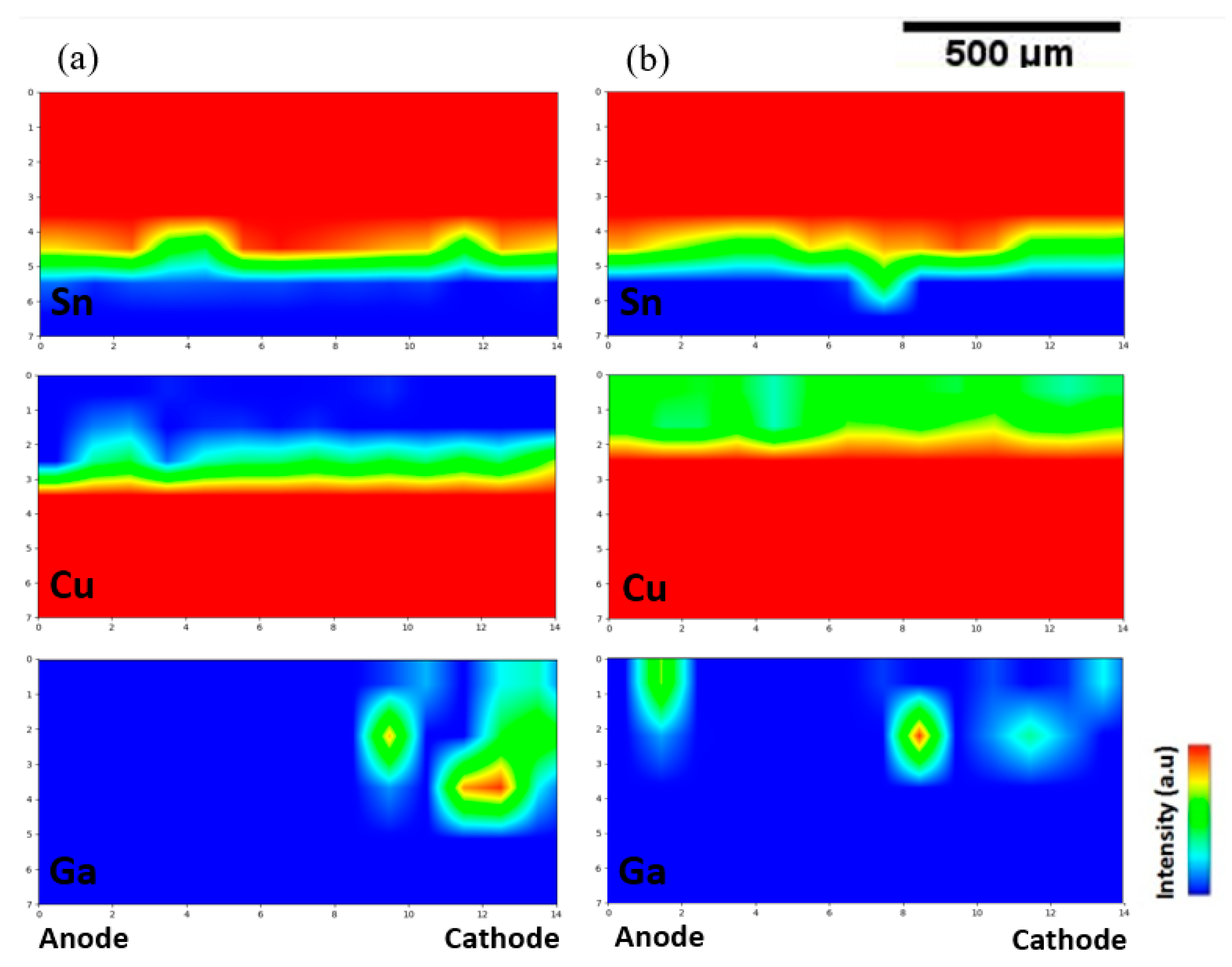
3.4. Synchrotron Micro-XRF

The elemental distribution was mapped using the synchrotron micro-XRF, as it allows for the identification of elements that are difficult to be accurately identified using conventional analysis methods such as energy dispersive X-ray (EDX) analysis. Figure 8 shows the elemental maps, and it can be seen that the main elements in the sample are Sn and Cu. Due to low signals, Ga is seen to be distributed randomly in the β–Sn region on both samples under electromigration with and without thermal ageing, as per Figure 8a,b. The bright red color represents the high concentration of the element in the marked area, while the dark blue color represents the element’s lowest concentration. It is believed that there is a migration of atom from cathode to anode. After the electromigration test (a), all atoms migrated to the anode, while Sn and Ga’s concentration decreased at the cathode. The diffusion of Sn atoms from the coating to the Cu lead frame was suppressed by the Ga elements in the Sn–0.7Cu–0.05Ga/Cu solder joint. Ga also slows Cu diffusion into bulk Sn. After electromigration with a thermal ageing test (b), the diffusion of Cu increased.

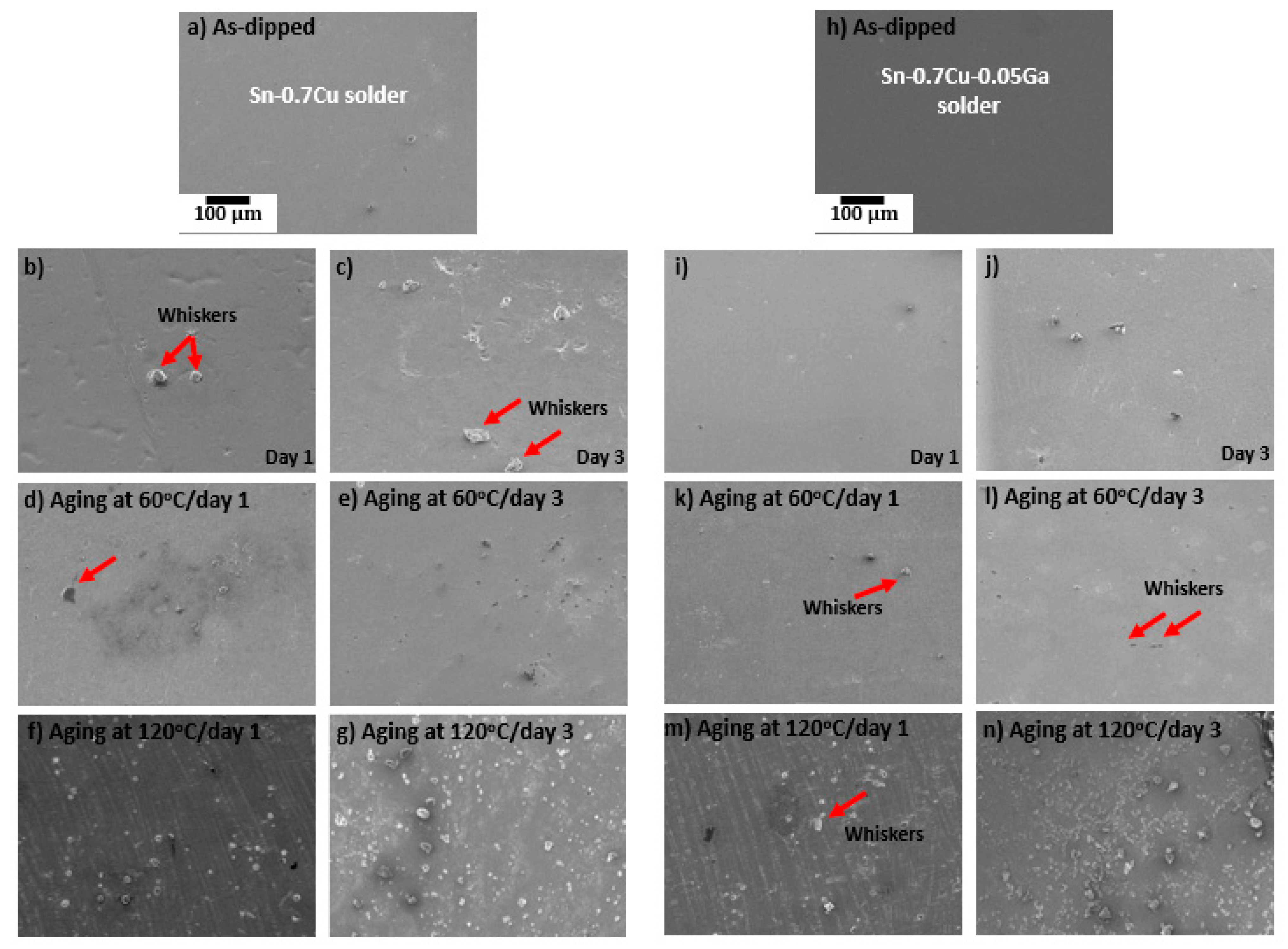
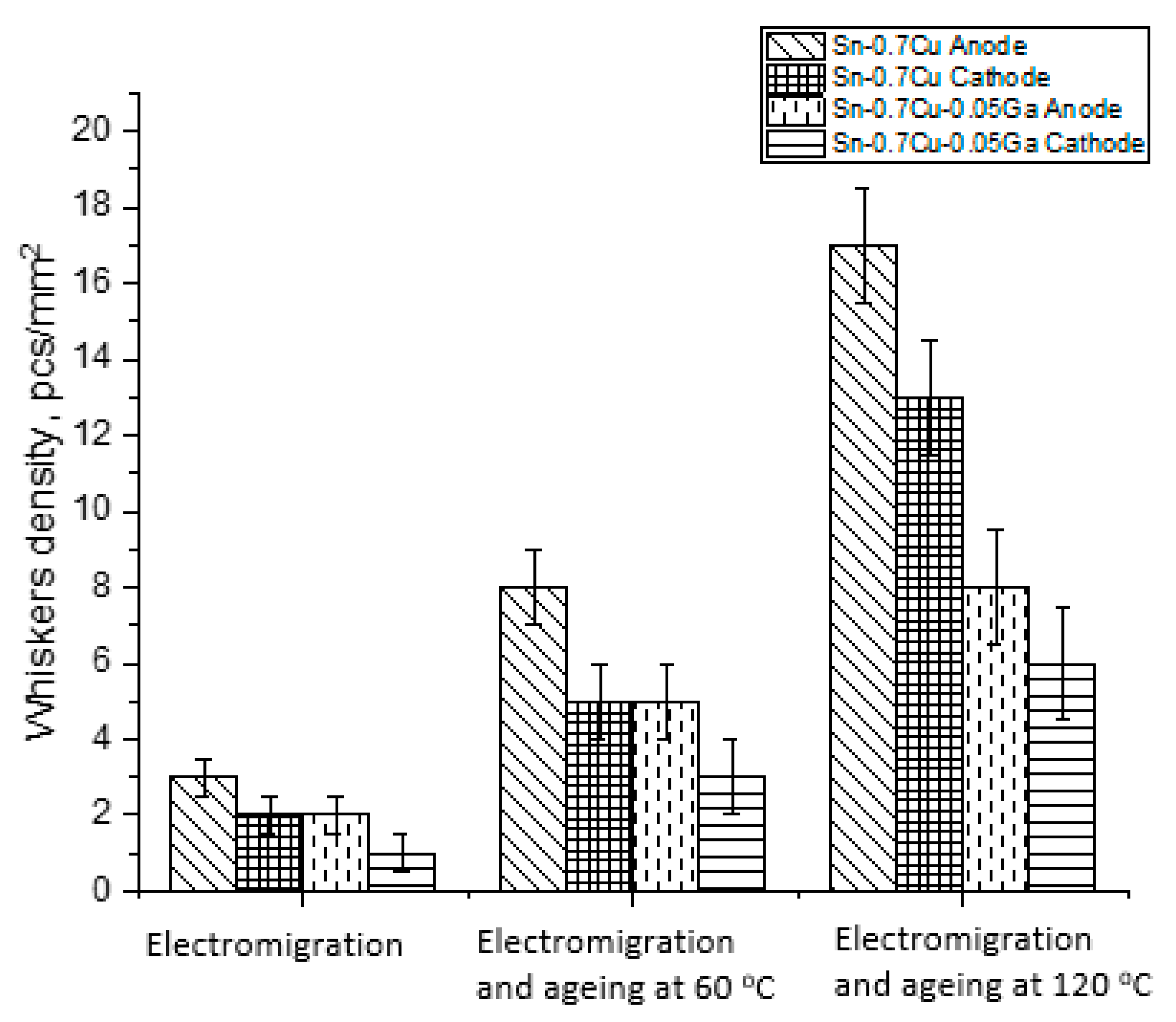
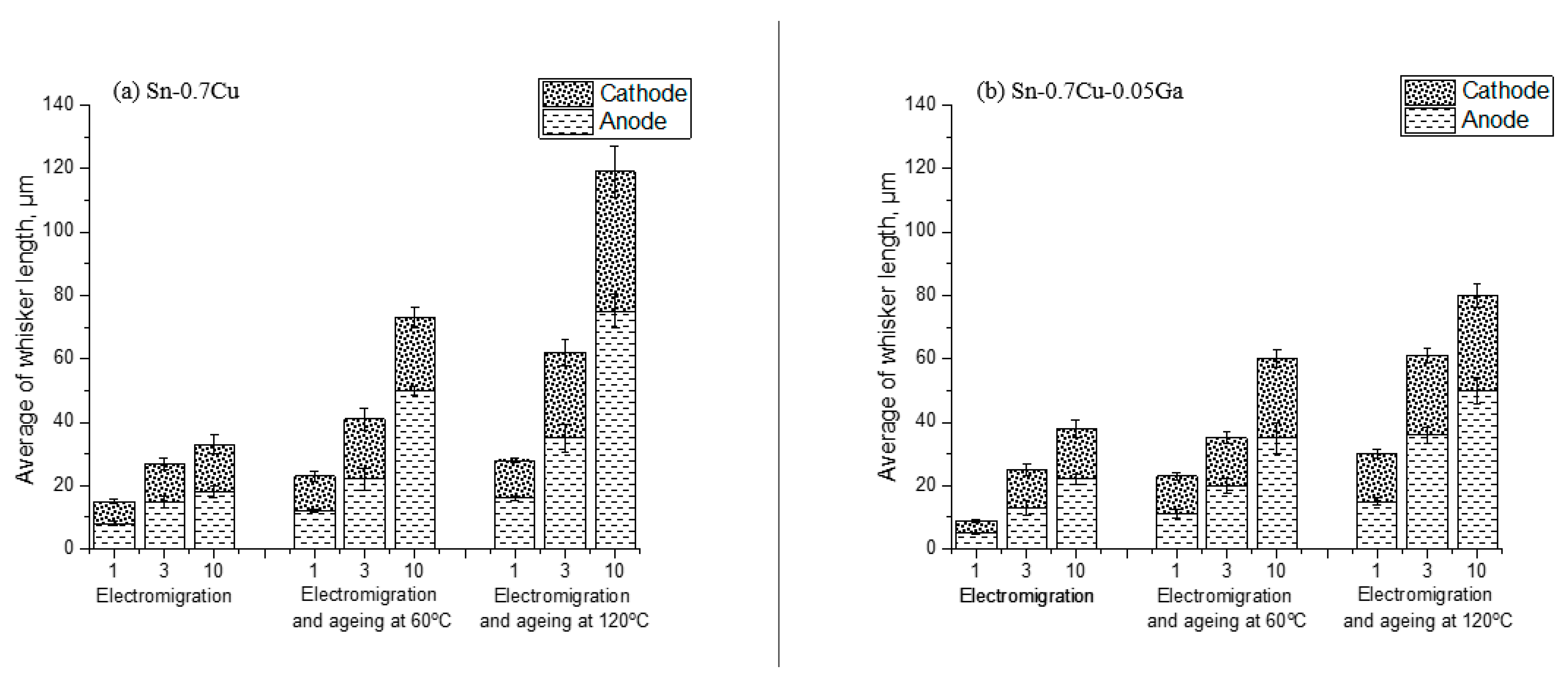
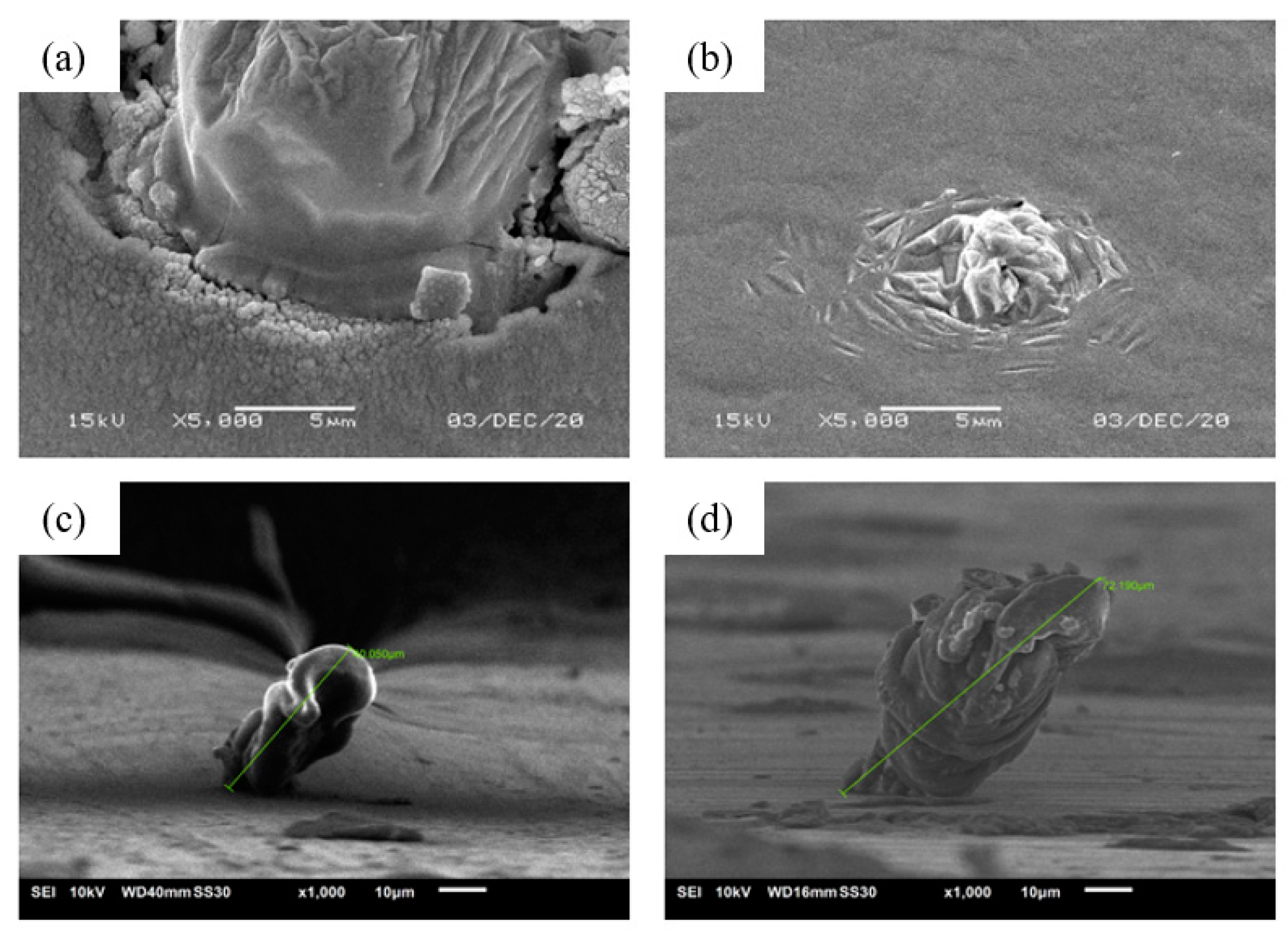
3.5. Properties of Tin Whiskers of the Solder

The morphology of the Sn whiskers was captured by JEOL JSM 6460LA scanning electron microscope (SEM) by JEOL Ltd. Tokyo, Japan. The samples were first accelerated by electromigration testing before their surface area was inspected. Different whisker growth behaviors of Sn on the Sn–0.7Cu and Sn–0.7Cu–0.05Ga solder materials under electromigration and electromigration with thermal ageing were seen, as shown in Figure 9. It can be seen that Sn whiskers were formed at the solders’ surface after being subjected to applied constant current for a day. In the beginning of the testing, only small whiskers were formed on Sn–0.7Cu dipped solder. The nodule-type whiskers began forming on the day 1 of the testing. It can be clearly observed from the image that the size of whiskers on Sn–0.7Cu solder had increased on day 3 of testing. When the samples had been thermally aged at 60 °C, the whiskers grew more after day 3. The highest number of whiskers were formed on the samples after current-stressed and aged at temperature of 120 °C on the same day. However, when the same conditions were applied to Sn–0.7Cu–0.05Ga, the growth showed fewer whiskers than the pure Sn–0.7Cu solders. Thus, the growth of Sn whiskers can be restrained by adding 0.05 wt.% Ga to the Sn–0.7Cu solders.
The average densities of the whiskers were plotted in Figure 10 using a quantitative measuring method. The number of whiskers is higher at anode side for all conditions. The average whisker density of the Sn–0.7Cu–0.05Ga was lower than the average whisker density of the Sn–0.7Cu. Initially, the lower whiskers on the cathode side happened because of the migration of atom from cathode to anode. After being thermally aged at 60 °C, the number of whiskers increased. When the temperature increased to 120 °C, the whisker density also increased. However, there was less whisker growth on the Sn–0.7Cu–0.05Ga solder’s surface, which could be due to Ga acting as a solid-solution strengthening agent. Ga also has an effect on Cu diffusion [21,25].
To further evaluate the effect of temperature on the length of whiskers, the tests were extended up to 10 days. Figure 11 plotted the length of the longest whiskers on the cathode and anode after electromigration with and without thermal ageing. From the data, the longest Sn whisker was observed on the surface of the Sn–0.7Cu sample stored at a temperature of 120 °C. The Sn whiskers of Sn–0.7Cu–0.05Ga solder on the cathode area had the shortest average length compared to the Sn whiskers on the Sn–0.7Cu solder.
In the beginning, after the electromigration testing, Sn whiskers in pure Sn–0.7Cu solder had a length of ~7–8 μm, while in the case of the Sn–0.7Cu–0.05Ga, the length of the whiskers was reduced to ~4–5 μm. The whiskers’ length on Sn–0.7Cu after being exposed for 3 days of current stressing was ~15–18 μm, while the whiskers’ length on the Sn–0.7Cu–0.05Ga was up to 15 µm. The maximum length of whiskers of pure Sn–0.7Cu and Sn–0.7Cu–0.05Ga solders increased gradually after constant current and exposed to 60 °C. Initially, the length of the whiskers of Sn–0.7Cu expanded up to 20 μm, while the whiskers length of Sn–0.7Cu–0.05Ga solders was only increased to 15 μm after 3 days of exposure. The whiskers’ length on cathode area had lower length compared to the length of whiskers on the anode side. After 10 days, the length of a single whisker for Sn–0.7Cu increased to 50 μm, and Sn–0.7Cu–0.05Ga up to 35 μm, respectively. This is because the diffusion of Cu atom increases the whiskers’ length, which simultaneously quickens the whiskers’ growth rate. When the temperature rises to 120 °C with the constant electric current, the whiskers’ length of Sn–0.7Cu increases to 70 μm on the anode side and 44 μm on the cathode side, while the whiskers of Sn–0.7Cu–0.05Ga increase to 50 μm on at the anode side and 30 μm on the cathode side. Ga’s addition to the pure Sn–0.7Cu solder mitigated whisker growth after the three conditions were applied to the samples. The highest density of whisker was observed on the surface of the Sn–0.7Cu sample at 120 °C. However, Sn–0.7Cu–0.05Ga produces fewer and shorter whiskers on the cathode area at room temperature.
The morphology of the whiskers is affected by the grain structure of the samples [34]. Hillocks are the pyramidal monocrystalline formed at the surface of the samples. They grow from the Sn matrix of the samples and can form a root to penetrate the solder layer. They can grow longer when there is a sufficient supply of Sn atom [22,35]. The minor alloying element of Ga also affects the growth of Sn whiskers on Sn–0.7Cu solder. The increasing temperature and the alloying element both reduce the length and slow down the whiskers’ growth. This result is in agreement with a study which stated that alloying with Fe and Bi on Sn–0.7Cu and ageing at high temperature result in fewer and shorter Sn whiskers [36].
In a study regarding electromigration mechanism [18], the high electric current produced massive atomic diffusion during electromigration in the electron flow direction [24]. The atomic flux drifted to the anode, and the equal flux of vacancies diffused to the cathode. The study showed both the atomic and electric carriers flow and cause interactions of thermal energy. This results in current crowding which occurs at the ends of the solder alloys during current stressing. The electromigration stress pushed Sn atoms from the cathode to the anode [23], resulting in compressive stress. The hillocks grew and extruded in the form of stress release. The whiskers’ growth is related to the stress relaxation at the Sn film’s weak spot, where the surface oxide was broken on the Sn surface [21,37]. The whiskers’ growth is initiated using the electric current stressing which is caused by the bombardment of the moving electrons. These moving electrons bombard the Sn atoms and drift them to the anode by a vacancy-mediated process.
The compressive stress is formed up at the anode. The whiskers in this area grow on the surface to release the stress when the compressive stress is too large to break the oxide’s surface. As a result, a hillock is formed when the broken area is too large. Nevertheless, it also has the potential to cause defects because the large and brittle intermetallic phases could initiate cracks. This degrades the solder join where the Sn whiskers extrude from the cracks to relax the compressive stress. Whisker growth observed on these types of samples is shown in Figure 12a,b. Figure 12c,d illustrate the typical size and morphology of the whiskers present on the surface under the JEDEC method. By comparing the results of the electromigration with and without thermal ageing, it can be concluded that the temperature of the ageing test is the main factor affecting the whiskers’ growth and the behavior of the solder coating. It is also linked to the IMC growth, which is the primary source of stress in the solder coating. On the other hand, samples with added Ga had thin IMC layers, which produced fewer whiskers. The schematic diagram of the mechanism of whiskers’ growth under electromigration and thermal ageing is illustrated in Figure 13.

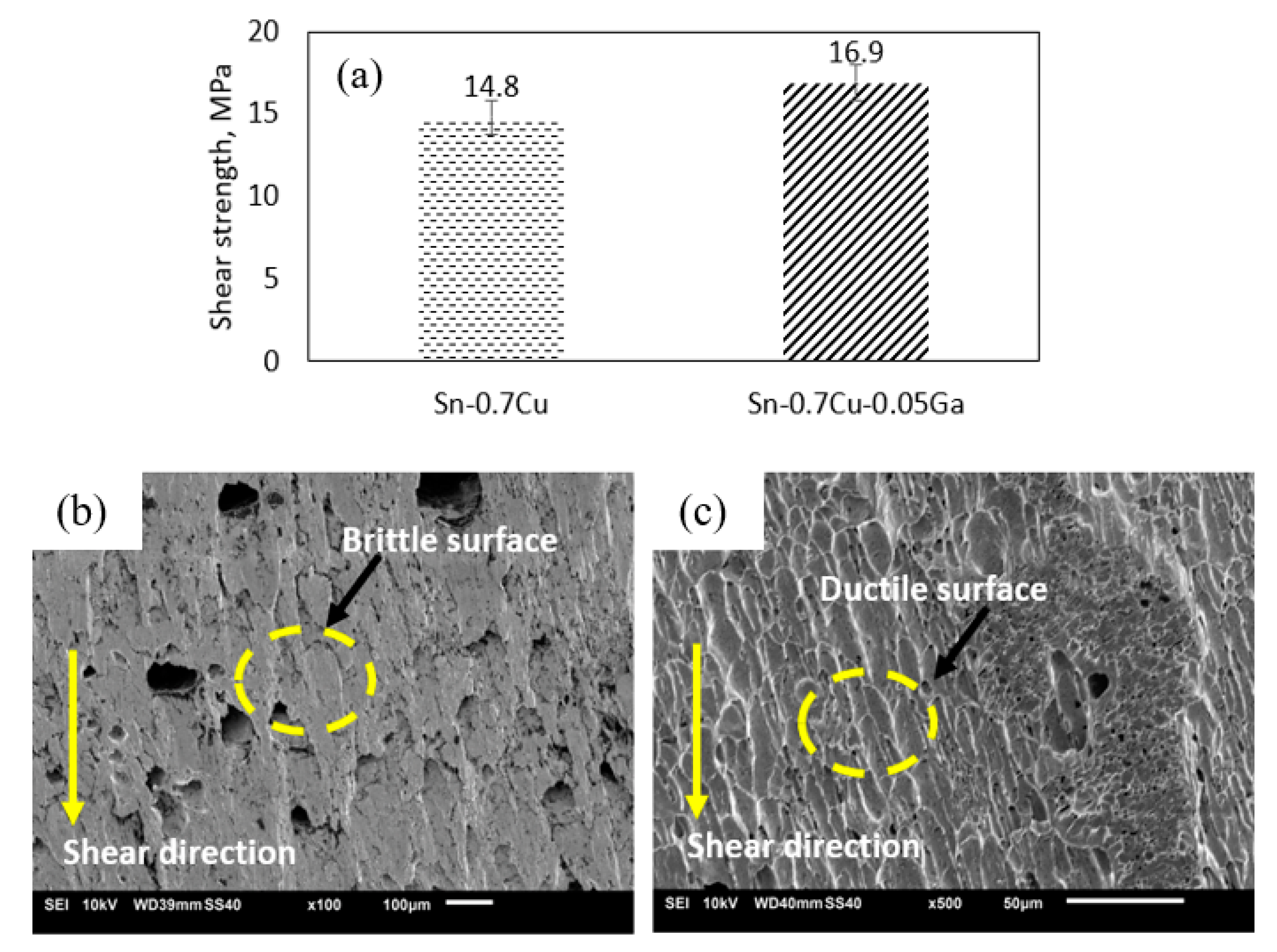
3.6. Mechanical Properties and Fracture Morphology

The mechanical performance of the Sn–0.7Cu–0.05Ga/Cu solder joint was determined by measuring its shear strength. The purpose is to provide a brief description of the performance of the solder composition. A single-lap shear test was performed in this study in order to simulate the actual solder joints in the electronic and microelectronic industries. Figure 14 shows the effect of the Ga addition on the mechanical properties. The shear strength of the Sn–0.7Cu solder was improved by adding 0.05 wt.% Ga. It was further enhanced to 16.9 MPa, which is a 14% improvement over the Sn–0.7Cu solder. The addition of Ga to the Sn–0.7Cu solder changes its microstructure. The changes in mechanical properties caused by Ga’s addition could be due to the β–Sn grain refinements and the finer IMC thickness (as shown in Figure 3). This is elucidated by the fracture morphology of the soldered joints. As shown in Figure 14b,c, generally, the fracture morphology of Sn–0.7Cu solder joints after tensile tests shows plenty of typical dimples with brittle fracture. Since no IMCs were found on the fracture morphology, it can be concluded that the fracture occurred at the solder itself. The dimples with a ductile fracture in the Sn–0.7Cu–0.05Ga solder joint were much finer than the ones in the Sn–0.7Cu solder, which confirms that the microstructural refinement is due to the addition of Ga. As seen in the grain refinement mechanism, the solder joints’ mechanical properties were improved. Generally, Ga alloying can decrease the IMC and whisker formation of Sn–0.7Cu solder with the improvement of its mechanical properties.

4. Conclusions

The study investigated the effects of electromigration with and without thermal ageing of 0.05 wt.% Ga addition to the Sn–0.7Cu solder. From the results, it can be concluded that:
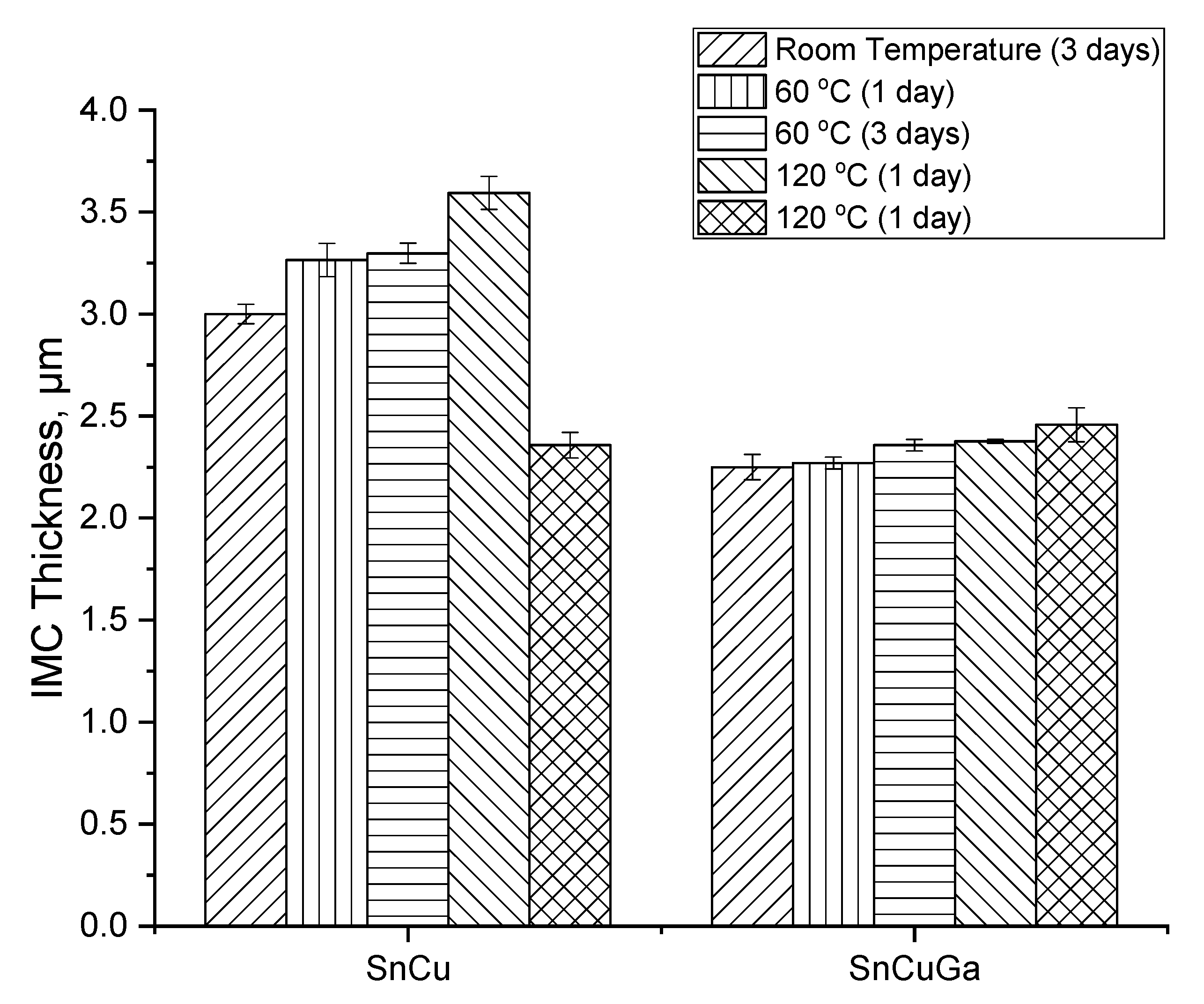
  • The thickness of the IMC of Sn–0.7Cu and Sn–0.7Cu–0.05Ga increased from 0.6% to 4.2%, corresponding with the increasing number of ageing temperature and ageing time.
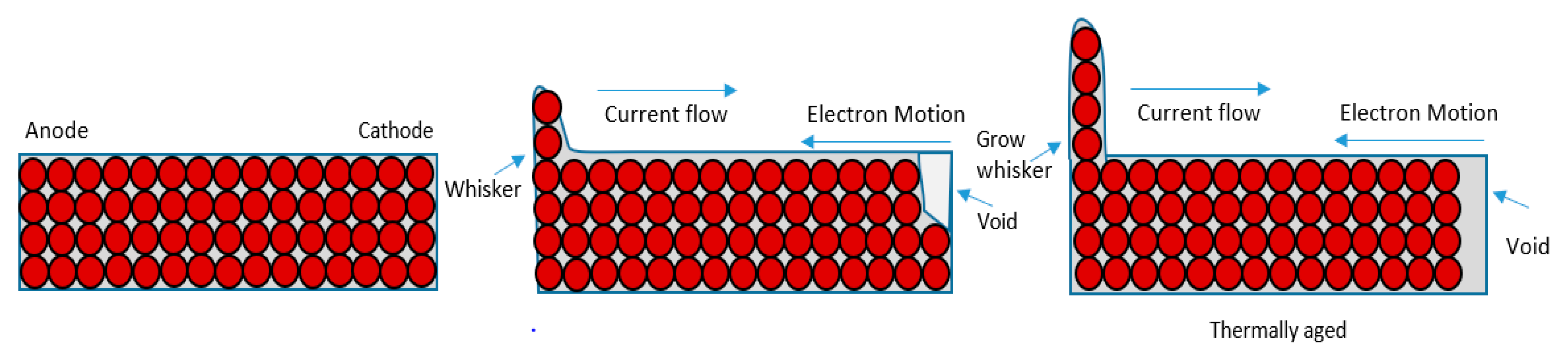
  • Whiskers’ growth was reduced with the addition of 0.05 wt.% of Ga, which also acted as a solid-solution strengthening agent.
  • The micro-XRF analysis showed the elemental distribution of Ga in Sn–0.7Cu–0.05Ga solder both under electromigration with and without thermal ageing. The distribution of Ga in the matrix decreases whiskers’ growth in the Sn–0.7Cu–0.05Ga solder joint.
  • The shear strength of the Sn–0.7Cu solder (14.8 MPa) improved by 14% due to Ga addition (~16.9 MPa).

Author Contributions

Conceptualization, methodology, and writing, N.Z.M.M.; supervision and resources, M.A.A.M.S.; methodology, formal analysis, and investigation, M.M.R.; methodology, A.V.S.; review and editing, J.C.; supervision and data curation, P.V.; review and editing, M.I.I.R. All authors have read and agreed to the published version of the manuscript.

Funding

The authors gratefully acknowledge Collaborative Research in Engineering, Science and Technology (CREST) under grant No. P14C1-17/001 with Nihon Superior for the materials and finance support.

Institutional Review Board Statement

Not applicable.

Informed Consent Statement

Not applicable.

Data Availability Statement

For data request, please contact corresponding author.

Acknowledgments

The authors gratefully acknowledge the support from Universiti Malaysia Perlis and Nihon Superior.

Conflicts of Interest

The authors declare no conflict of interest.

References

  1. Arnold, S.M. Repressing the Growth of Tin Whiskers. Plating 1966, 53, 96–99. Available online: https://hlinstruments.com/RoHS_articles/1966_Arnold_Repressing_Growth_of_Tin_Whiskers.pdf (accessed on 2 August 2021).
  2. Liang, J.; Dariavach, N.; Shangguan, D. Tin whisker nucleation and growth on Sn-Pb eutectic coating layer inside plated through holes with press-fit pins. IEEE Trans. Compon. Packag. Technol. 2008, 31, 152–158. [Google Scholar] [CrossRef]
  3. Wei, C.C.; Liu, P.C.; Chen, C. Electromigration-induced Pb and Sn whisker growth in SnPb solder stripes. J. Mater. Res. 2008, 23, 2017–2022. [Google Scholar] [CrossRef] [Green Version]
  4. Zhou, W.; Zhang, H.; Wu, P. Whisker growth in Sn and SnPb thin films under electromigration. Vacuum 2014, 107, 103–107. [Google Scholar] [CrossRef]
  5. Tu, K.; Zeng, K. Tin–lead (SnPb) solder reaction in flip chip technology. Mater. Sci. Eng. R Rep. 2001, 34, 1–58. [Google Scholar] [CrossRef]
  6. Ku, A.; Oetinscitan, O.; Saphores, J.-D.; Shapirod, A.; Schoenunp, J.M. Lead-free solders. Issues of toxicity, availability and impacts of extraction. In Proceedings of the 53rd Electronic Components and Technology Conference, New Orleans, LA, USA, 27–30 May 2003. [Google Scholar]
  7. Morris, J.W.; Goldstein, J.L.F.; Mei, Z. Microstructure and mechanical properties of Sn-In and Sn-Bi solders. JOM 1993, 45, 25–27. [Google Scholar] [CrossRef]
  8. Ramli, M.I.I.; Mohd Salleh, M.A.A.; Yasuda, H.; Chaiprapa, J.; Nogita, K. The effect of Bi on the microstructure, electrical, wettability and mechanical properties of Sn-0.7Cu-0.05Ni alloys for high strength soldering. Mater. Des. 2019, 186, 108281. [Google Scholar] [CrossRef]
  9. Xian, J.W.; Mohd Salleh, M.A.A.; Belyakov, S.A.; Su, T.C.; Zeng, G.; Nogita, K.; Gourlay, C.M. Influence of Ni on the refinement and twinning of primary Cu6Sn5 in Sn-0.7Cu-0.05Ni. Intermetallics 2018, 102, 34–45. [Google Scholar] [CrossRef]
  10. Cheng, S.; Huang, C.M.; Pecht, M. A review of lead-free solders for electronics applications. Microelectron. Reliab. 2017, 75, 77–95. [Google Scholar] [CrossRef]
  11. Zhao, M.; Zhang, L.; Liu, Z.-Q.; Xiong, M.-Y.; Sun, L. Structure and properties of Sn-Cu lead-free solders in electronics packaging. Sci. Technol. Adv. Mater. 2019, 20, 421–444. [Google Scholar] [CrossRef] [PubMed] [Green Version]
  12. Illés, B.; Krammer, O.; Hurtony, T.; Dušek, K.; Bušek, D.; Skwarek, A. Kinetics of Sn whisker growth from Sn thin-films on Cu substrate. J. Mater. Sci. Mater. Electron. 2020, 31, 16314–16323. [Google Scholar] [CrossRef]
  13. Chason, E.; Jadhav, N.; Pei, F.; Buchovecky, E.; Bower, A. Growth of whiskers from Sn surfaces: Driving forces and growth mechanisms. Prog. Surf. Sci. 2013, 88, 103–131. [Google Scholar] [CrossRef]
  14. Somidin, F.; Maeno, H.; Salleh, M.M.; Tran, X.Q.; McDonald, S.D.; Matsumura, S.; Nogita, K. Characterising the polymorphic phase transformation at a localised point on a Cu6Sn5 grain. Mater. Charact. 2018, 138, 113–119. [Google Scholar] [CrossRef]
  15. Hashim, A.N.; Salleh, M.A.A.M.; Mokhtar, N.Z.M.; Idris, S. Tin (Sn) whisker growth from electroplated Sn finished. IOP Conf. Ser. Mater. Sci. Eng. 2019, 701, 012005. [Google Scholar] [CrossRef]
  16. Xu, C.; Zhang, Y.; Fan, C.; Abys, J.A. Driving force for the formation of Sn whiskers: Compressive stress-pathways for its generation and remedies for its elimination and minimization. IEEE Trans. Electron. Packag. Manuf. 2005, 28, 31–35. [Google Scholar]
  17. Horváth, B. Influence of copper diffusion on the shape of whiskers grown on bright tin layers. Microelectron. Reliab. 2013, 53, 1009–1020. [Google Scholar] [CrossRef]
  18. Hsu, T.-Y.; Chang, J.-Y.; Chang, H.-M.; Ouyang, F.-Y. Electromigration induced spontaneous Ag whisker growth in fine Ag-alloy bonding interconnects: Novel polarity effect. Mater. Lett. 2016, 182, 55–58. [Google Scholar] [CrossRef]
  19. Mokhtar, N.Z.M.; Salleh, M.A.A.M.; Hashim, N.M. Preliminary Study of Electrical Current Stressing on Tin Whisker Formation. IOP Conf. Ser. Mater. Sci. Eng. 2019, 551, 012096. [Google Scholar] [CrossRef]
  20. Jin, Z.; Shen, Y.-A.; He, S.; Zhou, S.; Chan, Y.C.; Nishikawa, H. Novel polarity effect on intermetallic compound thickness changes during electromigration in Cu/Sn-3.0Ag-0.5Cu/Cu solder joints. J. Appl. Phys. 2019, 126, 185109. [Google Scholar] [CrossRef]
  21. Liu, S.H.; Chen, C.; Liu, P.C.; Chou, T. Tin whisker growth driven by electrical currents. J. Appl. Phys. 2004, 95, 7742–7747. [Google Scholar] [CrossRef] [Green Version]
  22. Fukuda, Y.; Osterman, M.; Pecht, M. The impact of electrical current, mechanical bending, and thermal annealing on tin whisker growth. Microelectron. Reliab. 2007, 47, 88–92. [Google Scholar] [CrossRef]
  23. Lin, S.K.; Liu, Y.C.; Chiu, S.J.; Liu, Y.T.; Lee, H.Y. The electromigration effect revisited: Non-uniform local tensile stress-driven diffusion. Sci. Rep. 2017, 7, 3082. [Google Scholar] [CrossRef]
  24. Guo, F.; Xu, G.; He, H.; Zhao, M.; Sun, J.; Wang, C.H. Effect of Electromigration and Isothermal Aging on the Formation of Metal Whiskers and Hillocks in Eutectic Sn-Bi Solder Joints and Reaction Films. J. Electron. Mater. 2009, 38, 2647. [Google Scholar] [CrossRef]
  25. Zhang, Q.K.; Long, W.M.; Yu, X.Q.; Pei, Y.Y.; Qiao, P.X. Effects of Ga addition on microstructure and properties of Sn–Ag–Cu/Cu solder joints. J. Alloy. Compd. 2015, 622, 973–978. [Google Scholar] [CrossRef]
  26. Ramli, M.I.I.; Mohd Salleh, M.A.A.; Mohd Sobri, F.A.; Narayanan, P.; Sweatman, K.; Nogita, K. Relationship between free solder thickness to the solderability of Sn–0.7Cu–0.05Ni solder coating during soldering. J. Mater. Sci. Mater. Electron. 2019, 30, 3669–3677. [Google Scholar]
  27. Somidin, F.; Salleh, M.A.A.; Ahmad, K.R. Intermetallic compound formation on solder alloy/cu-substrate interface using lead-free Sn-0.7Cu/recycled-aluminum composite solder. J. Adv. Mater. Res. 2013, 620, 105–111. [Google Scholar] [CrossRef]
  28. Yu, H.; Xin, Y.; Wang, M.; Liu, Q. Hall-Petch relationship in Mg alloys: A review. J. Mater. Sci. Technol. 2018, 34, 248–256. [Google Scholar] [CrossRef]
  29. Chen, K.I.; Cheng, S.C.; Cheng, C.H.; Wu, S.; Jiang, Y.-L.; Cheng, T.-C. The Effects of Gallium Additions on Microstructures and Thermal and Mechanical Properties of Sn-9Zn Solder Alloys. Adv. Mater. Sci. Eng. 2014, 2014, 606814. [Google Scholar] [CrossRef] [Green Version]
  30. Huang, Y.T.; Hsu, H.H.; Wu, A.T. Electromigration-induced back stress in critical solder length for three-dimensional integrated circuits. J. Appl. Phys. 2014, 115, 034904. [Google Scholar] [CrossRef]
  31. Lin, Y.W.; Lai, Y.S.; Lin, Y.L.; Tu, C.T.; Kao, C.R. Tin Whisker Growth Induced by High Electron Current Density. J. Electron. Mater. 2008, 37, 17–22. [Google Scholar] [CrossRef]
  32. Wang, F.; Liu, L.; Li, D.; Wu, M. Electromigration behaviors in Sn-58Bi solder joints under different current densities and temperatures. J. Mater. Sci. Mater. Electron. 2018, 29, 21157–21169. [Google Scholar] [CrossRef]
  33. Abdelhadi, O.M.; Ladani, L. IMC growth of Sn-3.5Ag/Cu system: Combined chemical reaction and diffusion mechanisms. J. Alloy. Compd. 2012, 537, 87–99. [Google Scholar] [CrossRef]
  34. Yu, C.-F.; Chan, C.-M.; Hsieh, K.-C. The effect of tin grain structure on whisker growth. Microelectron. Reliab. 2010, 50, 1146–1151. [Google Scholar] [CrossRef]
  35. Li, M.Y.; Yang, H.F.; Zhang, Z.H.; Gu, J.H.; Yang, S.H. Fast formation and growth of high-density Sn whiskers in Mg/Sn-based solder/Mg joints by ultrasonic-assisted soldering: Phenomena, mechanism and prevention. Sci. Rep. 2016, 6, 27522. [Google Scholar] [CrossRef] [Green Version]
  36. Jo, J.-L.; Nagao, S.; Hamasaki, K.; Tsujimoto, M.; Sugahara, T.; Suganuma, K. Mitigation of Sn Whisker Growth by Small Bi Additions. J. Electron. Mater. 2013, 43, 1–8. [Google Scholar] [CrossRef] [Green Version]
  37. Sarobol, P.; Pedigo, A.; Koppes, J.; Wang, Y.; Chen, W.; Su, P.; Handwerker, C. Whisker Formation and Stress Relaxation in Tin Thin Films. Microsc. Microanal. 2011, 17, 1846–1847. [Google Scholar] [CrossRef] [Green Version]
Figure 1. Schematic diagram of the electromigration and thermal ageing tests.
Coatings 11 00935 g001
Figure 2. The calculation of the IMC’s thickness.
Coatings 11 00935 g002
Figure 3. Optical micrograph of (a) Sn–0.7Cu, (b) Sn–0.7Cu–0.05Ga solder alloy at 50 × magnification. Top view of SEM micrograph of Cu6Sn5 grain structure after dipping at 300 °C for 3 s. Sn coating was etched away showing the morphology of Cu6Sn5 formed at Sn/Cu interface, (c) Sn–0.7Cu, (d) Sn–0.7Cu–0.05Ga.
Coatings 11 00935 g003
Figure 4. Average total IMC layer thickness of Sn–0.7Cu and Sn–0.7Cu–0.05Ga under room temperature condition.
Coatings 11 00935 g004
Figure 5. Intermetallic compound (IMC) formation of dipped solder after 3 days of electromigration: (a) Sn–0.7Cu at anode; (b) Sn–0.7Cu at cathode; (c) Sn–0.7Cu–0.05Ga at anode; (d) Sn–0.7Cu–0.05Ga at cathode.
Coatings 11 00935 g005
Figure 6. IMC formation of electromigration with thermal ageing of Sn–0.7Cu at (a) 60 °C for 1 day, (b) 60 °C for 3 days, (c) 120 °C for 1 day, and (d) 120 °C for 3 days; and Sn–0.7Cu–0.05Ga at (e) 60 °C for 1 day, (f) 60 °C for 3 days, (g) 120 °C for 1 day, and (h) 120 °C for 3 days.
Coatings 11 00935 g006
Figure 7. Average total IMC thickness of Sn–0.7Cu and Sn–0.7Cu–0.05Ga exposed by electromigration and thermal ageing at the anode side.
Coatings 11 00935 g007
Figure 8. Synchrotron micro-XRF mapping of Sn–0.7Cu–0.05 Ga: (a) Sn–0.7Cu–0.05Ga under electromigration, (b) Sn–0.7Cu–0.05Ga under electromigration and thermal ageing.
Coatings 11 00935 g008
Figure 9. Whisker growth on Sn–0.7Cu: (a) as-dipped solder; after day 3 electromigration testing (b,c); after thermal ageing at 60 °C on day 1 and day 3 (d,e); after thermal ageing at 120 °C on day 1 and day 3 (f,g). Whisker growth on Sn–0.7Cu–0.05Ga: (h) as-dipped solder; after day 3 electromigration testing (i,j); after thermal ageing at 60 °C on day 1 and day 3 (k,l); after thermal ageing at 120 °C on day 1 and day 3 (m,n).
Coatings 11 00935 g009
Figure 10. Sn whisker density of Sn–0.7Cu and Sn–0.7Cu–0.05Ga after electromigration with and without thermal ageing, with thermal ageing at 60 °C and 120 °C, at anode and cathode side after 3 days.
Coatings 11 00935 g010
Figure 11. The average length of Sn whiskers after electromigration with and without thermal ageing at 60 °C and 120 °C, at anode and cathode side, after 1, 3, and 10 days: (a) Sn–0.7Cu; (b) Sn–0.7Cu–0.05Ga.
Coatings 11 00935 g011
Figure 12. Different types of whiskers growing from Sn-based: (a) Sn whiskers formed from the crack region, (b) Sn whisker growth from compressive stress around it, (c,d) JEDEC measuring of irregular shape of whisker.
Coatings 11 00935 g012
Figure 13. Schematic diagram of tin whisker growth under electromigration and thermal ageing.
Coatings 11 00935 g013
Figure 14. Graph of (a) shear strength and SEM fracture surface image of (b) Sn–0.7Cu/Cu and (c) Sn–0.7Cu–0.05 wt.% Ga/Cu.
Coatings 11 00935 g014
Table 1. Test Conditions of the Testing.
Test TypePeriodTemperature
Electromigration1 day, 3 days30 °C
Electromigration and ageing 1, 3, and 10 days60 °C, 120 °C
Publisher’s Note: MDPI stays neutral with regard to jurisdictional claims in published maps and institutional affiliations.

