Article

Properties of RF Magnetron-Sputtered Copper Gallium Oxide (CuGa2O4) Thin Films

by
Ashwin Kumar Saikumar
*,
Sreeram Sundaresh
,
Shraddha Dhanraj Nehate
and
Kalpathy B. Sundaram
Department of Electrical and Computer Engineering, University of Central Florida, Orlando, FL 32816, USA
*
Author to whom correspondence should be addressed.
Coatings 2021, 11(8), 921; https://doi.org/10.3390/coatings11080921
Submission received: 6 July 2021 / Revised: 26 July 2021 / Accepted: 28 July 2021 / Published: 1 August 2021
(This article belongs to the Special Issue Advances in Thin Film Fabrication by Magnetron Sputtering)

Abstract

:
Thin films of CuGa2O4 were deposited using an RF magnetron-sputtering technique for the first time. The sputtered CuGa2O4 thin films were post-deposition annealed at temperatures varying from 100 to 900 °C in a constant O2 ambience for 1.5 h. Structural and morphological studies were performed on the films using X-ray diffraction analysis (XRD) and a Field Emission Scanning Electron Microscope (FESEM). The presence of CuGa2O4 phases along with the CuO phases was confirmed from the XRD analysis. The minimum critical temperature required to promote the crystal growth in the films was identified to be 500 °C using XRD analysis. The FESEM images showed an increase in the grain size with an increase in the annealing temperature. The resistivity values of the films were calculated to range between 6.47 × 10³ and 2.5 × 10⁸ Ωcm. Optical studies were performed on all of the films using a UV-Vis spectrophotometer. The optical transmission in the 200–800 nm wavelength region was noted to decrease with an increase in the annealing temperature. The optical bandgap value was recorded to range between 3.59 and 4.5 eV and showed an increasing trend with an increase in the annealing temperature.

1. Introduction

Wide-bandgap semiconductors such as Ga2O3, ZnO, indium tin oxide, HfO2, Y2O3, ZrO2, AlGa2O3, IGZO exhibit many attractive properties beyond the capabilities of Si, and hence find applications in electronics, optical, optoelectronics, photonics and magneto-electronic devices [1,2,3,4,5,6,7]. As a result, the research and development of metal oxides with versatile properties are imperative. Among the various metal-oxide materials, cubic spinels have attracted great attention due to their chemical structure consisting of tetrahedral and octahedral sites [8]. Cubic spinels with the formula AB2O4 have cations distributed randomly among one octahedral site and two tetrahedral sites. B3+ ions occupy half of the octahedral holes, and A2+ ions occupy one eighth of the tetrahedral holes [9]. One such cubic spinel material exhibiting a wide bandgap like Ga2O3 is CuGa2O4. The copper and gallium ions in CuGa2O4 are distributed randomly in the A and B sublattices. This pseudo-binary system consisting of CuO-Ga2O3 phases displays a high potential for optoelectronic applications. Furthermore, CuGa2O4 has distinguished physical and chemical stability and exhibits a catalytic property. The fundamental requirement to promote catalytic and photocatalytic properties demands control over the thin films regarding the particle size, surface area and crystallinity. Due to its high sensitivity and rapid response to reducing/oxidizing, CuGa2O4 is a noteworthy candidate material for gas sensing towards H2, liquefied petroleum and NH3 [10].
Due to its unique structure, CuGa2O4 finds applications in supercapacitors [11], and as an active catalyst for a hydrogen gas source [12], a photocatalyst for solar hydrogen production [13], anode materials for sodium-ion batteries [14], and in organic photovoltaic devices [15]. Previous studies have synthesized CuGa2O4 using techniques such as chemical vapor deposition (CVD), aerosol-assisted CVD [9], solid-state reaction [16], thermal decomposition [17], laser molecular beam epitaxy (L-MBE) [18] and hydrothermal techniques [19]. Synthesizing spinels requires multiple steps, high processing temperatures and a longer synthesis time [12,20]. Additionally, conventional CVD techniques involve volatile precursors, and the processes can be limited due to the formation of toxic byproducts. Among all of the thin-film deposition techniques, the magnetron sputtering technique is an established method of depositing thin films with high uniformity and homogeneity [1]. The magnetron sputtering techniques provide the flexibility to choose target materials with a wide range of melting points. This feature provides the capability to regulate the film thickness and deposition rate. Moreover, the magnetron sputtering technique does not demand the use of toxic or specialized precursors, which are required for CVD, and it offers great adhesion over a large surface area.
There have been no reported attempts to deposit CuGa2O4 thin films using the RF magnetron sputtering technique. This work addresses this inadequacy and focuses on the investigation of the properties of CuGa2O4 thin films synthesized using RF magnetron sputtering. Thin films of CuGa2O4 were deposited using a stoichiometric target mixture of Cu2O and Ga2O3 in the presence of argon gas. The influence of annealing the films in the presence of oxygen gas at different temperatures was evaluated. The chemical structure, morphological properties, optical properties and electrical properties of CuGa2O4 thin films were investigated.

2. Experimental

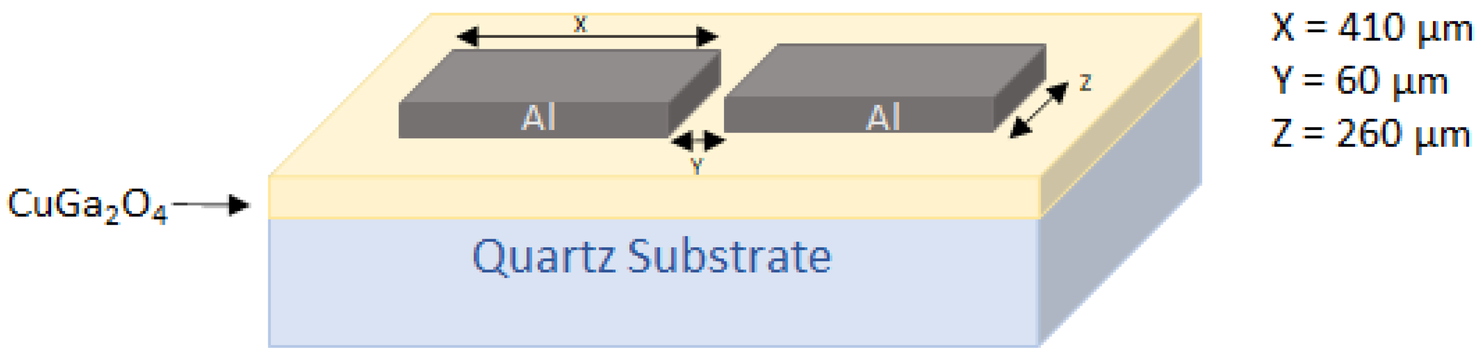
2.1. Deposition of the CuGa2O4 Thin Films

CuGa2O4 films were deposited using an ultra-high vacuum 3 gun sputtering system (AJA international, Scituate, MA, USA). Fused quartz substrates were used for the annealing of the films at temperatures above 500 °C, and regular glass substrates were used for the annealing of the films at temperatures lower than 500 °C. The substrates were cleaned using acetone, methanol and DI water, followed by drying using nitrogen gas. The CuGa2O4 films were deposited using a 3-inch powder pressed sputtering target with stochiometric proportions of Cu2O and Ga2O3 (99.99% purity). A base pressure of 3 × 10⁻⁷ Torr was achieved before every deposition. The sputter depositions were performed at the RF frequency (13.56 MHz) and a constant power of 200 W, using ultra-pure grade Ar as the sputtering gas. The Ar flow was kept constant at 10 sccm, and the deposition pressure was maintained constant at 10 mTorr for all of the depositions. All of the CuGa2O4 films reported in this research had a uniform thickness of 2000 Å. The substrate holder was rotated at a speed of 20 rpm in order to obtain a uniform thin-film thickness. All of the film depositions were performed at room temperature. The films were then annealed, post deposition, for 1.5 h at temperatures varying from 100 to 900 °C in O2 ambience. The O2 flow into the annealing furnace was maintained at 100 sccm for all of the film annealing.

2.2. Film Characterization

A Veeco Dektak 150 profilometer (Veeco, NY, USA) was used to measure the thickness of the films. The XRD measurements were performed using a PANalytical Empyrean XRD system (Malvern Panalytical, Westborough, MA USA), using radiation from a Cu source at 45 kV and 40 mA. The diffraction patterns were recorded between 2θ angles of 25–70°, and the phase information was analyzed using HighScore Plus software (Malvern Panalytical, Westborough, MA USA). The surface morphology of the film was identified using field emission scanning electron microscope Zeiss ULTRA-55 FEG SEM, (Zeiss Microscopy, White Plains, NY, USA). The optical transmission studies were performed using a Cary 100 UV-Vis spectrophotometer (Varian Analytical Instruments, Walnut creek, CA, USA). In order to perform the optical transmission studies, a wavelength range of 200–800 nm was used for the film deposited on the quartz substrates, and the wavelength range of 300–800 nm was used for the films deposited on the glass substrates. The resistivity of the film was measured by patterning parallel Al contact pads on the annealed CuGa2O4 films. In order to pattern the Al contact pads, a liftoff process was used. Once the contact pad windows were patterned, Al metal was deposited by adopting thermal evaporation. A schematic representation of the configuration used for the electrical measurements, along with the dimensions of the contact pads, is shown in Figure 1. A Keithley 2450 source meter (Tektronix Inc, Beaverton, OR, USA) unit was used to measure the I-V characteristics. From the measured I-V characteristics data, the resistance R was calculated. From the calculated R value, the resistivity (ρ) of the film was identified using the formula mentioned below:
ρ = R   A L
where R is the resistance, L is the length and A is the area of cross section.

3. Results and Discussions
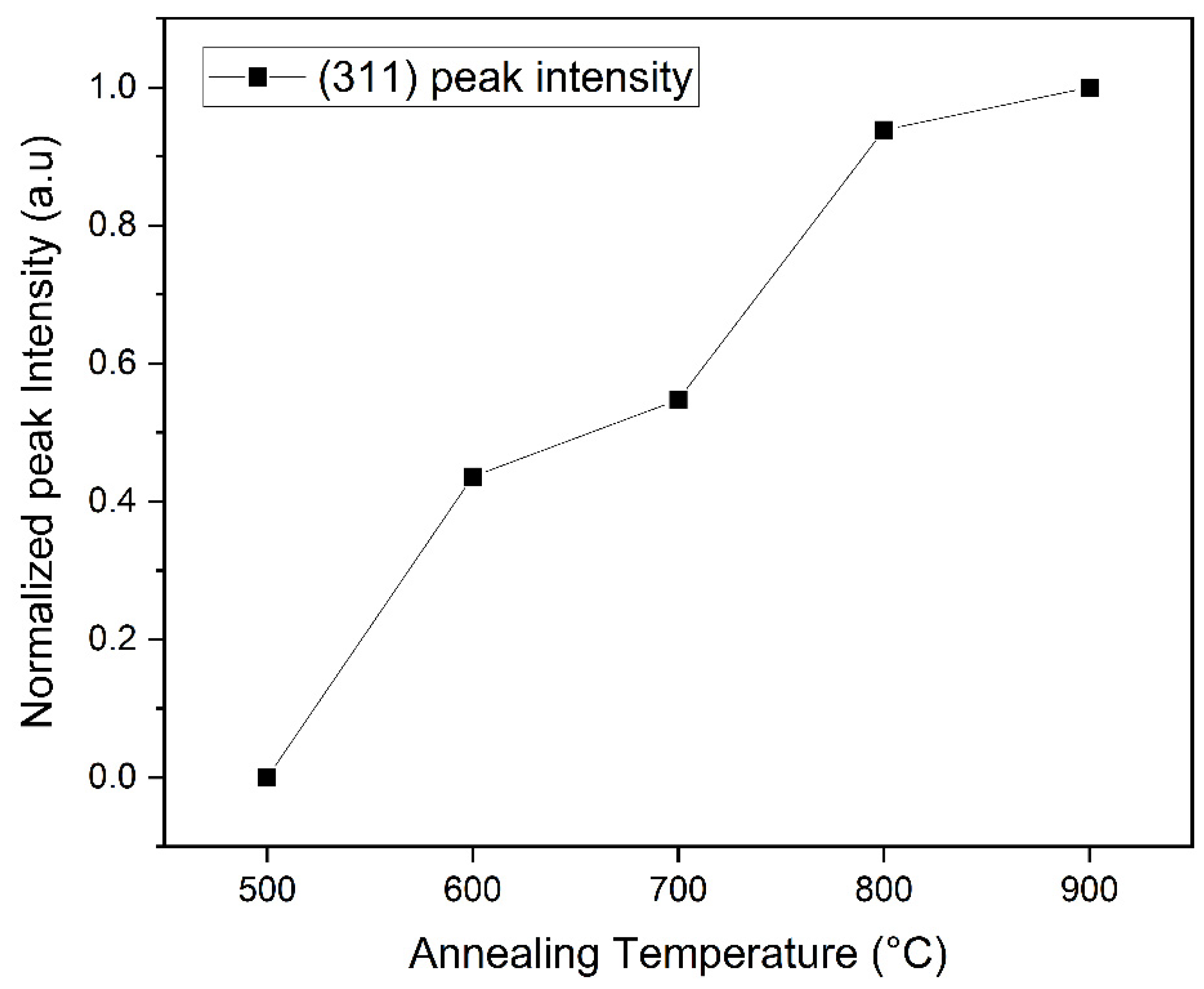
3.1. XRD Analysis

Thin-film XRD diffractograms of the as-deposited CuGa2O4 thin films, as well as films annealed at temperatures varying from 500–900 °C, are shown in Figure 2. The XRD pattern did not display any distinguished peaks for the as-deposited CuGa2O4 thin films or the thin films annealed at temperatures lower than 500 °C. However, the CuGa2O4 thin films annealed at temperatures of 500–900 °C displayed distinguishable peaks. The films annealed at 500 °C showed only two distinct peaks with comparatively lower intensity. They are the (311) peak related to the CuGa2O4 and (111) related to CuO. This suggests that the as-deposited films and the films annealed at temperatures less than 500 °C were majorly amorphous; therefore, for the sake of comparison, the XRD patterns of films annealed at 300 °C and 400 °C are not shown in Figure 2. It is likely that the films require a minimum annealing temperature of 500 °C in order to crystallize. The diffraction peaks identified from the XRD pattern were indexed well with the peaks pertaining to CuGa2O4 (JCPDS PDF # 44-0183). The peaks pertaining to CuO were also identified, suggesting the presence of mixed phases in the deposited thin films. Such a similar presence of CuO peaks along with CuGa2O4 has been previously reported in earlier research [9,20]. The major peaks identified at 2θ of 35.73, 37.68 and 63.59 were indexed to the (311), (222) and (440) phases of CuGa2O4. No peaks pertaining to Ga2O3 were identified. From Figure 2, a steady improvement in the peak intensity and peak sharpness can be noticed with the increase in the annealing temperature, thereby denoting a gradual improvement in the crystallinity. The peak intensity of the strongest peak (311) of CuGa2O4 was plotted as a function of the annealing temperature in Figure 3. A steady increase in the (311) peak intensity with an increase in the annealing temperature is evident from Figure 3.

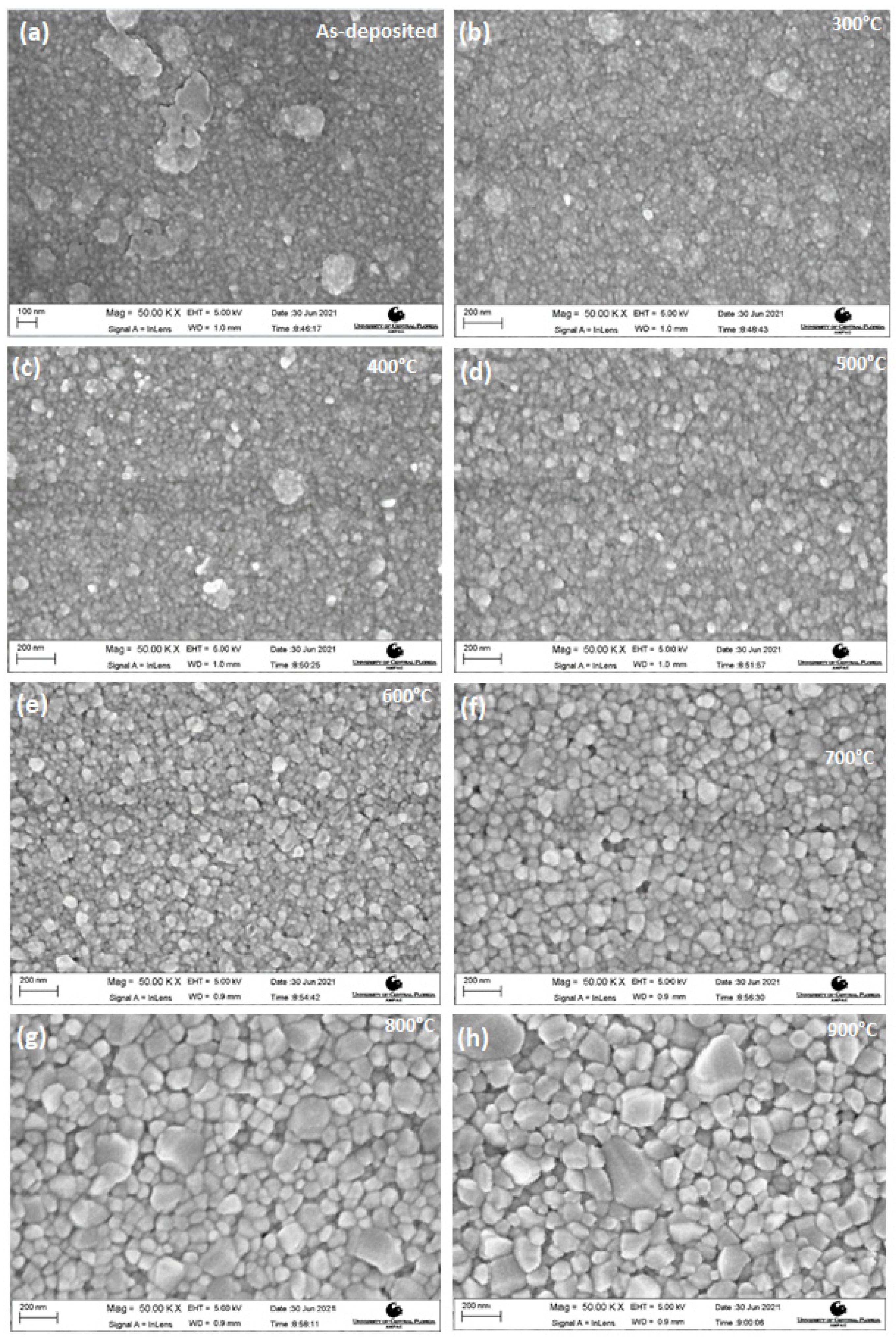
3.2. Morphology Studies

Figure 4 shows the FESEM images of the CuGa2O4 films. The morphological changes in both the as-deposited CuGa2O4 film (Figure 4a) and the CuGa2O4 films annealed at 300–900 °C (Figure 4b–h) can be seen clearly. Although the as-deposited film and films annealed at 300 °C and 400 °C displayed a tiny grain/particle presence in Figure 4a–c, they remained majorly amorphous and did not reveal any evidence of a peak presence in the XRD analysis. However, the film annealed at 500 °C displayed higher evidence of a grain presence and grain boundaries compared to the films annealed at 300 °C and 400 °C. This corroborates with the results from the XRD analysis in which the first appearance of diffraction peaks was observed in the film annealed at 500 °C. Deriving from the SEM findings and the appearance of diffraction peaks in the XRD analysis, it can be concluded that 500 °C is the minimum critical temperature required to promote nanocrystalline growth. The increase in the grain size with the increase in the annealing temperature can be evidently noted from Figure 4b–h. The small grains coalesce together and produce bigger grains when there is an increase in the annealing temperature [21]. This implies that the increment in the annealing temperature has an incremental influence on the CuGa2O4 film grain size. The film annealed at 900 °C was noted to have the largest-sized grains of 89 nm when compared to the other films. Figure 5 reiterates the steady increase in the grain size with the increase in the annealing temperature. The elemental analysis of all of the samples was performed using the EDAX incorporated in the FESEM. Table 1 shows the composition present in all of the films.

3.3. Optical Studies

3.3.1. Optical Transmission

The optical studies were performed on CuGa2O4 thin films deposited on quartz and glass substrates. Figure 6 shows the % transmission values recorded using a UV–Visible spectrophotometer in the wavelength range of 200–800 nm. The as-deposited CuGa2O4 thin films exhibited an optical transmission of ~60% at 500 nm. The increase in the annealing temperature resulted in the reduction of the optical transmission. The films annealed at 300 °C, 400 °C and 500 °C showed reduced transmission values between 30 and 40% at 500 nm. However, the higher annealing temperature further reduced the transmission from 60% for the as-deposited film to 30% for the film annealed at 600 °C, at the wavelength of 500 nm. This reduction in the optical transmission of CuGa2O4 thin films was attributed to a change in the grain size, as seen from the XRD analysis and FESEM images. The films with a low grain size were more transparent, while the optical transmission reduces with the annealing temperatures, as there is an increase in the grain size and crystallinity [22,23]. A further increase in the annealing temperature from 600 °C to 900 °C did not show much variation in the optical transmission of the CuGa2O4 thin films.

3.3.2. Optical Bandgap

The optical transmission data was used to calculate the optical bandgap of the CuGa2O4 thin films. The absorption coefficient (α) was calculated using the following equation:
α = ( 2.303 t ) log 10 ( % T )
where t is the thickness of the CuGa2O4 thin films, and T is the transmission. The optical bandgap (Eg) was estimated [24] using the following equation:
( α h ν ) 1 n = B   ( h ν E g )
where hν is the photon energy, B is a constant and Eg is the optical bandgap.
Figure 7 shows the Tauc plot generated using Equations (2) and (3). The linear region of the curves was extrapolated to the x-axis in order to achieve the Eg value. The optical bandgap values displayed an increasing trend with an increase in the annealing temperature. The bandgap of as-deposited film was 3.59 eV, which increased to 4.5 eV for the CuGa2O4 thin film annealed at 900 °C. The bandgap values obtained in this study are comparable to the bandgap values reported for CuGa2O4 thin films deposited using the laser MBE technique [18]. Table 2 shows the variation in the optical bandgap as a function of the annealing temperature. The unique structure and wide bandgap make CuGa2O4 a potential candidate material for ultraviolet optoelectronic device applications [18].

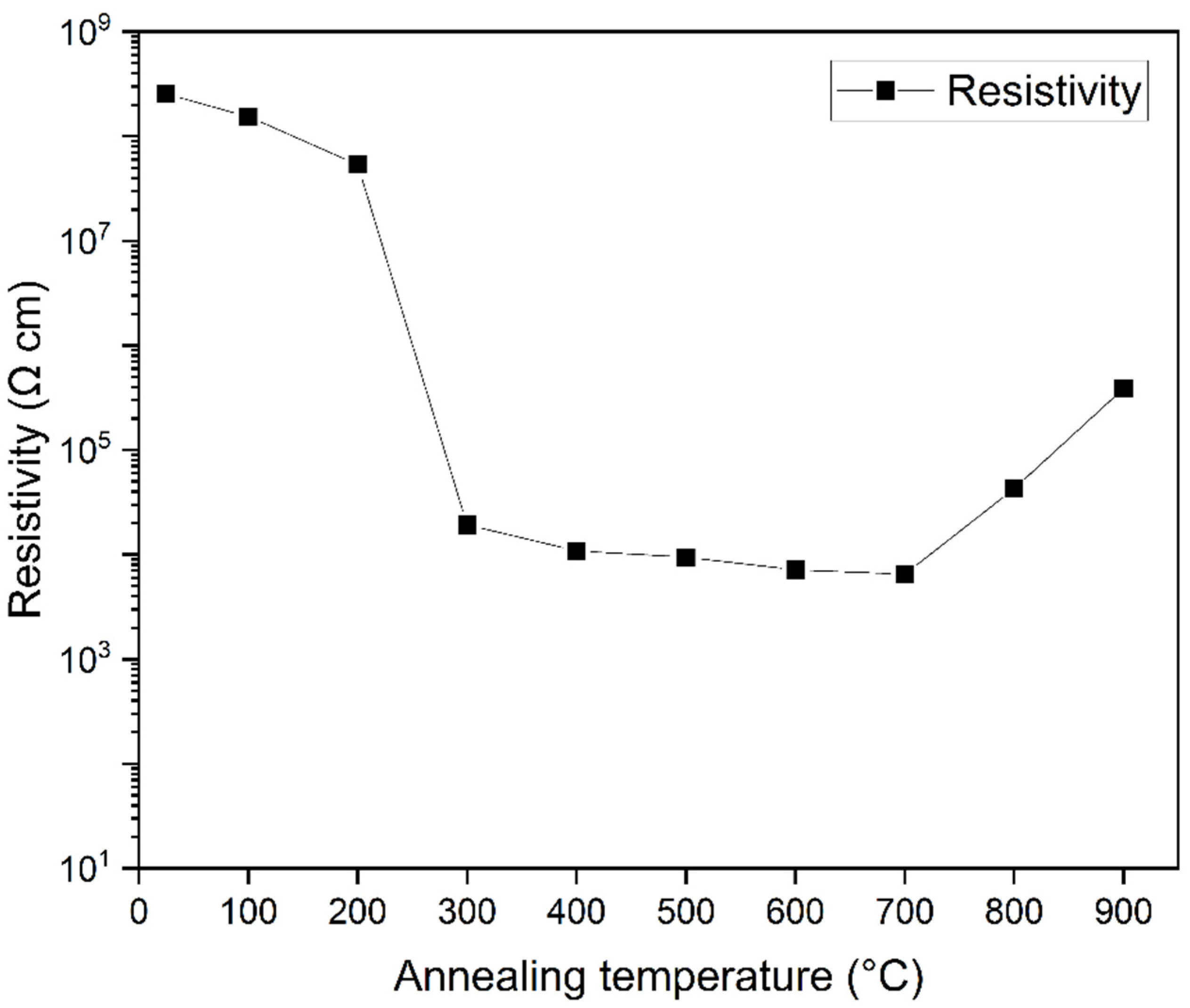
3.4. Electrical Studies

Figure 8 shows the electrical resistivity of the CuGa2O4 films. The electrical resistivities were calculated using the electrical resistance values obtained from the I–V curves. From Figure 8, it is evident that the resistivity showed a decreasing trend with increase in the annealing temperature up until 700 °C (6.4 × 10³ Ωcm). This reduction in resistivity could be ascribed to the crystallization of the films. However, the resistivity increased in the films annealed at higher temperatures, with the film annealed at 900 °C showing a higher resistivity of 3.89 × 10⁵ Ωcm. Such similar trends of decreasing resistivity up until a particular annealing temperature, followed by a subsequent increase in the resistivity at higher temperatures have been reported for other compounds belonging to the cubic spinel family [25]. Because there are no observed changes in the structural diffraction phases of the annealed films, the effect of annealing on the resistivity is primarily related to the grain density and grain boundaries. A similar increase in resistivity at very high annealing temperatures, despite with steady increase in the diffraction peak intensity (XRD peaks), has been previously reported in compounds belonging to the cubic spinel family [26,27]. One of the two plausible reasonings behind the increase in resistivity at higher temperatures is the decrease in the actual number of grains per volume, as noted from the FESEM image, thereby resulting in reduced carrier transitions [21,28]. This would potentially result in a resistivity increase. The other reason could be the presence of CuO phases in the film. Research conducted by Valladares et al. showed a sudden increase of resistivity in CuO films annealed at a temperature of 800 °C and above [29]. The authors attribute the increase in resistivity to the potential defects in the film. Similarly, the CuGa2O4 films sputtered in this research also showed an increase in resistivity in the films annealed at temperatures 800 °C and 900 °C.

4. Conclusions

In this study, thin films of copper gallium oxide spinel, CuGa2O4, were successfully deposited using a sputtering target with a stochiometric composition of Cu2O and Ga2O3 by an RF sputtering technique. The structural, morphological, optical and electrical effects due to post-deposition annealing of the CuGa2O4 thin films at temperatures varying from 100 to 900 °C in constant O2 ambience were examined using XRD, FESEM, UV-Vis spectrophotometer and I–V curves. The XRD peaks pertaining to both CuGa2O4 and CuO were identified from the XRD studies. It was found that a minimum critical temperature of 500 °C was required to promote the crystallization of the films. The crystallinity of the films was noted to improve with increase in the annealing temperature. The average grain size was recognized to increase from 30 nm to 89 nm when the annealing temperature was increased from 500 °C to 900 °C. The optical bandgap recorded an increments from 3.59 eV to 4.5 eV in the non-annealed films and the films annealed at 900 °C, respectively. The tunability of the electrical resistivity of the CuGa2O4 thin films as a function of the annealing temperature was demonstrated. The CuGa2O4 films showed a stark decrease in resistivity from the highest value of 2.5 × 10⁸ Ωcm in the as-sputtered films to the lowest resistivity of 6.47 × 10³ Ωcm in the films annealed at 700 °C. Due to its high bandgap and cubic structure, CuGa2O4 could potentially be used extensively in UV optoelectronic device applications.

Author Contributions

Conceptualization, A.K.S. and K.B.S.; methodology, A.K.S.; validation, A.K.S. and K.B.S.; investigation, A.K.S.; writing—original draft preparation, A.K.S.; writing—review and editing, A.K.S., S.S., S.D.N., K.B.S.; visualization, A.K.S.; supervision, K.B.S. All authors have read and agreed to the published version of the manuscript.

Funding

This research received no external funding.

Institutional Review Board Statement

Not applicable.

Informed Consent Statement

Not applicable.

Data Availability Statement

Data available on request.

Conflicts of Interest

The authors declare no conflict of interest.

References

  1. Saikumar, A.K.; Nehate, S.D.; Sundaram, K.B. RF sputtered films of Ga2O3. ECS J. Solid State Sci. Technol. 2019, 8, Q3064. [Google Scholar] [CrossRef]
  2. Saikumar, A.K.; Skaria, G.; Sundaram, K.B. ZnO gate based MOSFETs for sensor applications. ECS Trans. 2014, 61, 65. [Google Scholar] [CrossRef]
  3. Nehate, S.D.; Prakash, A.; Mani, P.D.; Sundaram, K.B. Work Function Extraction of Indium Tin Oxide Films from MOSFET Devices. ECS J. Solid State Sci. Technol. 2018, 7, P87–P90. [Google Scholar] [CrossRef]
  4. Mudavakkat, V.; Atuchin, V.; Kruchinin, V.; Kayani, A.; Ramana, C. Structure, morphology and optical properties of nanocrystalline yttrium oxide (Y2O3) thin films. Opt. Mater. 2012, 34, 893–900. [Google Scholar] [CrossRef]
  5. Pearton, S.; Abernathy, C.; Norton, D.; Hebard, A.; Park, Y.; Boatner, L.; Budai, J. Advances in wide bandgap materials for semiconductor spintronics. Mater. Sci. Eng. R Rep. 2003, 40, 137–168. [Google Scholar] [CrossRef] [Green Version]
  6. Saikumar, A.K.; Nehate, S.D.; Sundaram, K.B. A review of recent developments in aluminum gallium oxide thin films and devices. Rev. Solid State Mater. Sci. 2021, 1–32. [Google Scholar]
  7. Sanctis, S.; Hoffmann, R.C.; Koslowski, N.; Foro, S.; Bruns, M.; Schneider, J.J. Aqueous Solution Processing of Combustible Precursor Compounds into Amorphous Indium Gallium Zinc Oxide (IGZO) Semiconductors for Thin Film Transistor Applications. Chem. Asian J. 2018, 13, 3912–3919. [Google Scholar] [CrossRef] [PubMed]
  8. Petrakovskii, G.A.; Aleksandrov, K.S.; Bezmaternikh, L.N.; Aplesnin, S.S.; Roessli, B.; Semadeni, F.; Amato, A.; Baines, C.; Bartolomé, J.; Evangelisti, M. Spin-glass state in CuGa2O4. Phys. Rev. B 2001, 63, 184425. [Google Scholar] [CrossRef] [Green Version]
  9. Knapp, C.E.; Prassides, I.D.; Sathasivam, S.; Parkin, I.P.; Carmalt, C.J. Aerosol-Assisted Chemical Vapour Deposition of a Copper Gallium Oxide Spinel. ChemPlusChem 2013, 79, 122–127. [Google Scholar] [CrossRef] [PubMed]
  10. Shi, J.; Liang, H.; Xia, X.; Li, Z.; Long, Z.; Zhang, H.; Liu, Y. Preparation of high-quality CuGa2O4 film via annealing process of Cu/β-Ga2O3. J. Mater. Sci. 2019, 54, 11111–11116. [Google Scholar] [CrossRef]
  11. Zardkhoshoui, A.M.; Davarani, S.S.H. Designing a flexible all-solid-state supercapacitor based on CuGa2O4 and FeP-rGO electrodes. J. Alloy. Compd. 2019, 773, 527–536. [Google Scholar] [CrossRef]
  12. Faungnawakij, K.; Shimoda, N.; Fukunaga, T.; Kikuchi, R.; Eguchi, K. Cu-based spinel catalysts CuB2O4 (B= Fe, Mn, Cr, Ga, Al, Fe0. 75Mn0. 25) for steam reforming of dimethyl ether. Appl. Catal. A Gen. 2008, 341, 139–145. [Google Scholar] [CrossRef]
  13. Gurunathan, K.; Baeg, J.-O.; Lee, S.M.; Subramanian, E.; Moon, S.-J.; Kong, K.-J. Visible light active pristine and Fe3+ doped CuGa2O4 spinel photocatalysts for solar hydrogen production. Int. J. Hydrog. Energy 2008, 33, 2646–2652. [Google Scholar] [CrossRef]
  14. Pilliadugula, R.; Nithya, C.; Krishnan, N.G. Influence of Ga2O3, CuGa2O4 and Cu4O3 phases on the sodium-ion storage behaviour of CuO and its gallium composites. Nanoscale Adv. 2020, 2, 1269–1281. [Google Scholar] [CrossRef] [Green Version]
  15. Wang, J.; Ibarra, V.; Barrera, D.; Xu, L.; Lee, Y.-J.; Hsu, J.W.P. Solution Synthesized p-Type Copper Gallium Oxide Nanoplates as Hole Transport Layer for Organic Photovoltaic Devices. J. Phys. Chem. Lett. 2015, 6, 1071–1075. [Google Scholar] [CrossRef] [PubMed]
  16. Fenner, L.A.; Wills, A.S.; Bramwell, S.T.; Dahlberg, M.; Schiffer, P. Zero-point entropy of the spinel spin glasses CuGa2O4and CuAl2O4. J. Phys. Conf. Ser. 2009, 145. [Google Scholar] [CrossRef] [Green Version]
  17. Biswas, S.K.; Sarkar, A.; Pathak, A.; Pramanik, P. Studies on the sensing behaviour of nanocrystalline CuGa2O4 towards hydrogen, liquefied petroleum gas and ammonia. Talanta 2010, 81, 1607–1612. [Google Scholar] [CrossRef] [PubMed]
  18. Wei, H.; Chen, Z.; Wu, Z.; Cui, W.; Huang, Y.; Tang, W. Epitaxial growth and characterization of CuGa2O4 films by laser molecular beam epitaxy. AIP Adv. 2017, 7, 115216. [Google Scholar] [CrossRef] [Green Version]
  19. Yin, H.; Shi, Y.; Dong, Y.; Chu, X. Synthesis of spinel-type CuGa2O4 nanoparticles as a sensitive non-enzymatic electrochemical sensor for hydrogen peroxide and glucose detection. J. Electroanal. Chem. 2021, 885, 115100. [Google Scholar] [CrossRef]
  20. Gingasu, D.; Mindru, I.; Patron, L.; Marinescu, G.; Tuna, F.; Preda, S.; Calderon-Moreno, J.M.; Andronescu, C. Synthesis of CuGa2O4 nanoparticles by precursor and self-propagating combustion methods. Ceram. Int. 2012, 38, 6739–6751. [Google Scholar] [CrossRef]
  21. Ahmadipour, M.; Ain, M.F.; Ahmad, Z.A. Effects of annealing temperature on the structural, morphology, optical properties and resistivity of sputtered CCTO thin film. J. Mater. Sci. Mater. Electron. 2017, 28, 12458–12466. [Google Scholar] [CrossRef]
  22. Shakti, N.; Gupta, P.S. Structural and optical properties of sol-gel prepared ZnO thin film. Appl. Phys. Res. 2010, 2, 19. [Google Scholar] [CrossRef] [Green Version]
  23. Ramana, C.V.; Smith, R.J.; Hussain, O.M. Grain size effects on the optical characteristics of pulsed-laser deposited vanadium oxide thin films. Phys. Status Solidi 2003, 199, R4–R6. [Google Scholar] [CrossRef]
  24. Tauc, J.; Grigorovici, R.; Vancu, A. Optical Properties and Electronic Structure of Amorphous Germanium. Phys. Status Solidi 1966, 15, 627–637. [Google Scholar] [CrossRef]
  25. Li, R.; Fu, Q.; Zou, X.; Zheng, Z.; Luo, W.; Yan, L. Mn-Co-Ni-O thin films prepared by sputtering with alloy target. J. Adv. Ceram. 2020, 9, 64–71. [Google Scholar] [CrossRef] [Green Version]
  26. Schulze, H.; Li, J.; Dickey, E.C.; Trolier-McKinstry, S. Synthesis, Phase Characterization, and Properties of Chemical Solution-Deposited Nickel Manganite Thermistor Thin Films. J. Am. Ceram. Soc. 2009, 92, 738–744. [Google Scholar] [CrossRef]
  27. Kukuruznyak, D.A.; Bulkley, S.A.; Omland, K.A.; Ohuchi, F.S.; Gregg, M.C. Preparation and properties of thermistor thin-films by metal organic decomposition. Thin Solid Films 2001, 385, 89–95. [Google Scholar] [CrossRef]
  28. Ohyama, M.; Kozuka, H.; Yoko, T. Sol-Gel Preparation of Transparent and Conductive Aluminum-Doped Zinc Oxide Films with Highly Preferential Crystal Orientation. J. Am. Ceram. Soc. 2005, 81, 1622–1632. [Google Scholar] [CrossRef]
  29. Valladares, L.D.L.S.; Salinas, D.H.; Dominguez, A.B.; Najarro, D.A.; Khondaker, S.; Mitrelias, T.; Barnes, C.; Aguiar, J.A.; Majima, Y. Crystallization and electrical resistivity of Cu2O and CuO obtained by thermal oxidation of Cu thin films on SiO2/Si substrates. Thin Solid Films 2012, 520, 6368–6374. [Google Scholar] [CrossRef]
Figure 1. Schematic representation of the configuration used for the electrical measurements.
Coatings 11 00921 g001
Figure 2. X-ray diffractions of the as-deposited CuGa2O4 thin film and the CuGa2O4 thin films annealed at 500–900 °C in O2 ambience for 1.5 h.
Coatings 11 00921 g002
Figure 3. (311) peak intensity identified in the CuGa2O4 films as a function of the annealing temperature.
Coatings 11 00921 g003
Figure 4. FESEM images of (a) the as-deposited CuGa2O4 films and the CuGa2O4 films annealed at (b) 300 °C, (c) 400 °C, (d) 500 °C, (e) 600 °C, (f) 700 °C, (g) 800 °C and (h) 900 °C (SEM magnification were constant at 50 KX. All scales in the image are in nm range).
Coatings 11 00921 g004
Figure 5. Average grain size as a function of the annealing temperature.
Coatings 11 00921 g005
Figure 6. Optical transmission spectra of the CuGa2O4 thin films annealed at different temperatures.
Coatings 11 00921 g006
Figure 7. Tauc plot of the CuGa2O4 thin films annealed at different temperatures.
Coatings 11 00921 g007
Figure 8. Influence of the annealing temperature on the electrical resistivity.
Coatings 11 00921 g008
Table 1. CuGa2O4 film composition as a function of the annealing temperature, measured using EDAX.
FilmCu atm%Ga atm%O atm%
As deposited film13.6425.8860.48
Annealed at 300 °C14.9224.9060.18
Annealed at 400 °C14.7824.0761.15
Annealed at 500 °C13.9320.2165.86
Annealed at 600 °C14.1020.7965.11
Annealed at 700 °C14.5620.4365.01
Annealed at 800 °C13.8819.9266.19
Annealed at 900 °C13.1219.7167.16
Table 2. Optical bandgap values obtained for CuGa2O4 thin films.
Annealing TemperatureEg, Bandgap (eV)
As deposited3.59
100 °C3.72
200 °C3.76
300 °C3.8
400 °C3.84
500 °C4.12
600 °C4.36
700 °C4.4
800 °C4.44
900 °C4.5
Publisher’s Note: MDPI stays neutral with regard to jurisdictional claims in published maps and institutional affiliations.

