Abstract
Micro-filters fabricated using integration methods is now the trend for multichannel filters in imaging spectrum systems. Traditional multichannel bandpass filters are mainly fabricated separately by multilayered thin films and then glued together. This approach involves the complexity of precision cutting, dicing, and adhesive bonding; therefore, the possibility of miniaturization is quite limited. In this work, a dual channel bandpass thin film filter for the mid-infrared was fabricated by using the lift-off process. The structure of a 4-cavity Fabray–Perot (F-P) type filter was designed and optimized. The bandpass filter over the range 3.55–3.75 µm with full width at half maximum (FWHM) of 274 nm and the bandpass filter over the range 4.85–4.95 µm with FWHM of 246 nm were obtained with a 4.5 µm joint width. The average transmittance of the filters is more than 83.5% and optical density value of the cutoff is 3. The thickness of 3.55–3.75 µm bandpass filter was measured and the thickness error was analyzed. The results show that the thickness error, especially the thickness error of spacer layers, induces the degradations of peak transmission and bandwidth. This kind of mid-infrared filter has important application in space remote sensing, military, and civil fields.
1. Introduction
Multispectral imaging is a new generation of photoelectric detection technology which captures image data within specific wavelength ranges across the electromagnetic spectrum. The wavelengths may be separated by filters or detected by using instruments which are sensitive to particular wavelengths. Multispectral imaging combines the rich spectral information of a target with the spatial image of targets, improves the dimension of image information thus extends the function of traditional detection technology. Multispectral imaging was developed by National Aeronautics and Space Administration (NASA) [1,2] for space-based imaging and now is used in a variety of biomedical, food and agriculture, aerospace and defense, industrial, cultural heritage, and scientific applications [3].
The traditional spectral imaging system, such as dispersive prism system, diffraction grating system, and multiple camera system has a slow scan speed, a large size, and a high cost. However, the multichannel bandpass filter system has a smaller size, simplified structure and is lightweight. Multichannel bandpass filters played a crucial role in the multispectral imaging system. Figure 1 shows the schematic diagram of the filter. The width of a single channel is more than 0.5 mm and the joint width between two channels is more than 10 µm [4]. These kinds of filters are widely applied in the space spectral instrument [4]. The filter is firstly fabricated for every different passing band, and then the substrates are cut into long strips or other geometrical shapes, and finally glued together to obtain the multichannel filter. Owing to the precise cutting and adhesive bonding technique that are essential to this process, therefore, the degree of miniaturization is quite limited [5].
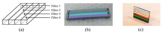
Figure 1.
(a) Schematic diagram of glued multichannel filter; (b,c) sample pictures of the multichannel filter.
In recent years, some new technology was applied to fabricate the multichannel filter such as electroforming [6], combinatorial etching technique [7,8], and lift-off process [8]. Red color filters [6] and three multichannel filters in the visible wavelengths with narrow bandwidth [9] were prepared. Lift-off processes were used to fabricate micro-arrayed multichannel optical filter mosaic. The optical filter mosaic consists of 4 different optical filters in visible wavelengths [10].
Compared with visible/near infrared filter, the mid infrared (3–5 µm) filter is difficult to fabricate because of the larger thickness, which also make it difficult for striping the photoresist in the lift-off process.
The 3–5 µm band is an important infrared window and it has important application in the space remote sensing field and military and civil field such as detection and evaluation of fire, intelligent seeker, recognition of military disguise, etc. For this application, much work has been done to fabricate the multichannel filter in the mid infrared spectral region. In the published work, the peak transmittance (Tmax) ranges from 30% to 65% [11,12]. A mid-IR dual-band filter, which consists of periodic gold grating and a CaF2 substrate, was prepared with the wavelength of ~3.8392 μm and the FWHM of 1.8 nm [13]. A bandpass infrared interference filter with sufficiently narrow bandwidth was developed. The filter has a passband width of 6 nm or 0.14% with peak transmission of 55% and a central wavelength of approximately 4.0 µm [14]. A six-channel fan-shaped integrated narrow-band filter on a silicon substrate was designed and fabricated [11]. Its average peak transmission reached 83.3%, the cut-off transmittance was less than 1% (optical density, OD = 2). Due to process limitations, most of the existing integrated filter arrays use a single-cavity F-P filter film system design, which yields a triangular-shaped transmittance spectral curve. Such filter spectral curves have low passband transmittance, narrow passband half-width and low cutoff, which decrease the S/N ratio when it is applied in test devices. Therefore, it is necessary to develop a multichannel with a high transmittance, a suitable bandwidth, high OD and joint width meeting the engineering demand.
In this work, a dual-channel bandpass filter for the mid-infrared was prepared, and the structure of the 4-cavity Fabry–Perot (F-P) type filter was designed and optimized. The filter was fabricated by using the traditional multiple thin-film vacuum deposition and the modern microlithography technologies (lift-off process). The transmittance, morphology, and cross-sectional scanning electron microscopy (SEM) of the filter were measured. The transmittance deviation of measured and designed data was analyzed.
2. Design
2.1. Design of the Bandpass Filters
For the conventional Fabry–Perot etalon, the metallic reflecting layers should be replaced by all-dielectric multilayers to improve the performance; the schematic diagram of an all-dielectric filter is shown in Figure 2. This is the single cavity structure of an all-dielectric Fabry–Perot filter. Basically, this is the same as the conventional etalon with dielectric coatings and with a solid thin-film spacer [7,15]. In this work, the dual channel bandpass filters were designed based on the Fabry–Perot structure.
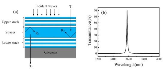
Figure 2.
(a) Schematic diagram of an all-dielectric F-P type filter and (b) its typical transmittance spectrum.
Transmittance of the filter with varying wavelengths is as follows [16]:
where R1 and R2, T1 and T2 are the reflectance and transmittance of the films stack, respectively, φ1 and φ2 are the reflection phase shift of the film stack, δ is the effective phase thickness of the spacer layer, n is the refractive index of the film, d is the physical thickness of the film, λ is the reference wavelength. When (φ1 + φ2 − 2δ)/2 = kπ (k = 0, ±1, ±2, ±3…), the transmittance value of the whole film stack reaches the maximum.
Figure 3a displays the calculated transmittance of bandpass filter for the region 3.55–3.75 µm with the primary structure. It was found that the thin-film F-P filter has a pass band shape which is triangular, and it is possible to modify this by coupling simple filters in series in much the same way as tuned circuits. These coupled arrangements are known as multiple cavity filters.
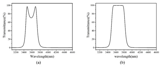
Figure 3.
(a) Calculated transmittance of bandpass filter for the region 3.55–3.75 µm with the primary structure. The substrate is double-polished silicon (n = 3.5); H = germanium (n = 4.0), L = zinc sulfide (n = 2.35) and the incident medium is air (n = 1.0). (b) Calculated transmittance of bandpass filter for the region 3.55–3.75 µm with the optimized structure.
Figure 3b shows the calculated transmittance of bandpass filter for the region 3.55–3.75 µm with the optimized structure. Compared with single cavity filters, the multiple cavity filters can improve the steepness of the pass-band and the optical density value in the cutoff band of the filter, thus, the S/N ratio applied of test devices will be improved. A F-P bandpass interference filter is built from alternating quarter-wave layers of high- and low-index transparent materials to achieve a high transmission only in a narrow band. For the middle infrared(MIR), germanium as the high-index material (H) and zinc sulfide as the low-index material (L) were used in this design. As these two materials have a significant difference in refractive index, matching stress and low absorbance coefficient in the wavelength of 3–5 µm, which can decrease the film thickness, increases the maximum transmittance values, and improves the stability of the filter.
For the bandpass filter over the range of 3.55–3.75 µm, the primary structure of the designed 4-cavity filter is Si/(HL) 2H (LH) L (HL) 2H (LH) L (HL) 2H (LH) L (HL) 2H (LH) L/Air, the reference wavelength λ0 is 3580 nm, where nsi = 3.5, H = 0.25λ0 (optical thickness) of index 4.0, L = 0.25λ0 (optical thickness) of index 2.35. Figure 3a gives the calculated transmittance of the filter. In order to improve the transmittance further, the primary structure was optimized as Si/(1.063H0.998L) 2H (LH) 1.485L (HL) 2H (LH) L (HL) 2H (LH) 1.535L (HL) 2H (1.162L1.323H) 1.087L/Air, the transmittance of optimized structure is shown as Figure 3b. Figure 3b shows the pass band profile of a 4-cavity filter is a square shape and the transmittance values approached 100% with the FWHM of 339 nm. The filters consist of 24 layers and the total film thickness is 8.7 µm.
Similarly, for the bandpass filter over the range 4.85–4.95 µm, the primary structure of the designed 4-cavity filter is Si/(HL) 2H (LH) L (HL) 4H (LH) L (HL) 4H (LH) L (HL) 2H (LH) L/Air, the reference wavelength λ0 is 4950 nm, where nsi = 3.5, H = 0.25λ0 (optical thickness) of index 4.0, L = 0.25λ0 (optical thickness) of index 2.35. Figure 4a gives the calculated transmittance of the filter. In order to improve the transmittance further, the primary structure was optimized as Si/(1.002H1.045L) 2H (LH) 0.601L (HL) 4H (LH) 1.050L (HL) 4H (LH) 0.624L (HL) 2H (L1.913H) 1.063L/Air, the transmittance of the optimized structure is shown as Figure 4b. Figure 4b shows the pass band profile of a 4-cavity filter is a square shape and the transmittance values approached 100% with the FWHM of 318 nm. The filters consist of 24 layers and the total film thickness is 12.5 µm.
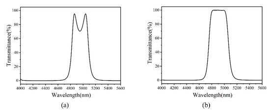
Figure 4.
(a) Calculated transmittance of bandpass filter for the region 4.85–4.95 µm with the primary structure. The substrate is double-polished silicon (n = 3.5); H = germanium (n = 4.0), L = zinc sulfide (n = 2.35) and the incident medium is air (n = 1.0). (b) Calculated transmittance of bandpass filter for the region 4.85–4.95 µm with the optimized structure.
In addition, double-layer antireflection coatings were deposited on the backside of the substrate to increase the transmittance. The structure is Si/2.45L0.809M/air, the reference wavelength λ0 is 5200 nm, where nsi = 3.5, L = 0.25λ0 (optical thickness) of index 2.35(ZnS), M = 0.25λ0 (optical thickness) of index 1.5 (YF3). The average transmittance of the antireflection coatings is more than 98% in our interested wavelength band.
2.2. Design of Lift-Off Process
The lift-off process refers to the process of exposing a pattern into photoresist, depositing a thin film over the entire area, then washing away the photoresist to leave behind the film only in the patterned area. Lift-off process has significant advantages in fabricating the linear or array filter with small cell size and joint width (micron grade) between the different cells when combined with the thin film technology.
The detailed process steps are shown in Figure 5: (1) spin coater (IMECAS, Beijing, China) is used to spin photoresist of the thickness of 10 µm after the substrate is cleaned. (2) Lithography machine (QUINTEL, San Jose, CA, USA) is used for exposure to obtain the sidewall undercut profile followed by the development. (3) The bandpass filter for the region 3.55–3.75 µm is deposited. (4) The photoresist remover and Supersonic Cleaner are used to strip the photoresist. (5) Step (1) is repeated. (6) The alignment accuracy of 0.5 µm and exposure is retained. (7) The bandpass filter for the region 4.85–4.95 µm is deposited. (8) Step (4) is repeated and the filter sample is obtained.
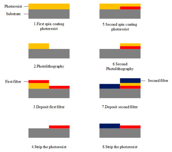
Figure 5.
The schematic diagram of detailed lift-off process steps.
3. Experiment and Characterization
All the thin films were deposited by Leybold SYRUS C1110 (Alzenau, Germany). Firstly, the single layer of Ge (purity 99.999%, granulate, Umicore JuBo, Beijing, China) and ZnS (purity 99.99%, granulate, CVD quality, Umicore) were deposited on double-polished silicon substrate, respectively, by changing the deposited process parameters such as the substrate temperature, evaporation rate, ion source bias, discharge current. The transmittance of the samples was measured by BRUKER VERTEX 70V (Ettlingen, Germany), then their optical properties (refractive index, extinction coefficient) were obtained by Material Editor software (version 2.71) based on their infrared spectra. The deposited parameters are shown as Table 1.

Table 1.
The deposition parameters of thin films.
Quintel 4000-4 (QUINTEL, San Jose, CA, USA) lithography machine was used for exposure, negative photoresist NR7-6000PY ((Futurrex, Franklin, NJ, USA) and Resist Removers RR9 (Futurrex, Franklin, NJ, USA) were used in the lift-off process. NR7-6000PY has a high temperature resistance of 180 °C. Spin coater KW-4A (IMECAS, Beijing, China) was used to spin the photoresist. Zeiss GeminiSEM 500 (Jena, Germany) and Hitachi SU1510 SEM (Naka, Japan) were used to observe the cross-section of the sample. Nikon Eclipse LV150NA microscope (Tokyo, Japan) was used to observe the surface morphology. The ultraviolet irradiation was tested by homemade equipment.
4. Results and Discussion
4.1. The Thickness of the Photoresist
Figure 6 presents the relationship between the spin speed, spin time and the thickness. It was found that the thickness decreases with the increasing of spin speed and the spin time. The photoresist thickness of 10 µm was obtained at the spin speed of 1500 rpm and spin time of 30 s. It is worth noting that if the photoresist thickness is decreased, it is difficult to strip the photoresist in the lift-off process. Conversely, if the photoresist thickness is increased, it causes more edge effect and increases the joint width between the two channels.
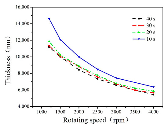
Figure 6.
The relationship between the spin speed, spin time and the thickness.
4.2. Sidewall Undercut Structure and Surface Morphology
The lift-off process requires the sidewall undercut profile of the photoresist. It is critical to strip the photoresist successfully. Figure 7 gives the lift-off process and illustrates the importance of the sidewall undercut structure. In order to obtain the sidewall undercut structure, the exposure and develop time should be accurately adjusted. The exposure time especially determined a sloping of the photoresist profile in the exposed region. Figure 8 demonstrates that insufficient exposure time (70 s) can cause the erosion of the remaining photoresist on the bottom; the overexposure time (74 s) can increase the bottom photoresist width which has a negative impact on the lift-off process. Therefore, a moderated exposure time (72 s) is critical.
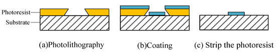
Figure 7.
Lift-off process: (a) photolithography to obtain the sidewall undercut profile of the photoresist. (b) Thin-film deposition, the top and bottom films become unconnected. (c) The top film can be lifted during photoresist strip.
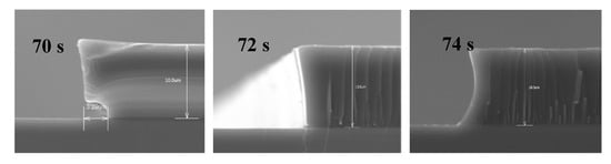
Figure 8.
The SEM of different sidewall profile with the exposure time. Insufficient exposure time (70 s); moderated exposure time (72 s); the overexposure (74 s).
Figure 9 gives the microscope photos of the two samples with different develop times. For negative photoresist, the insufficient develop time (50 s) causes the unexposed areas (especially in the marginal area) photoresist to not dissolve completely, which is also undesirable for the lift-off process. The develop time of 55 s is a suitable parameter for the lift-off process.
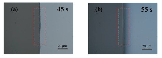
Figure 9.
The microscope photos of the two samples with different develop times: (a) 45 s, undeveloped, residual photoresist in the marginal area; (b) 55 s, develop, no residual photoresist.
4.3. Dual Channel Bandpass Thin Film Filter
The sample of dual channel bandpass thin film filter with different widths of channels is shown in Figure 10. The green color area is the 3.55–3.75 µm filter, the blue color area is the 4.85–4.95 µm filter, the substrate is 2 inch double-polished silicon wafer.
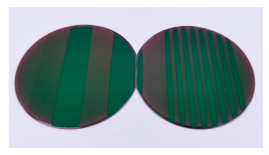
Figure 10.
The sample of dual channel bandpass thin film filter with different widths of channels. The green color area is the 3.55–3.75 µm filter, the blue color area is the 4.85–4.95 µm filter, the substrate is 2 inch double-polished silicon wafer.
The microscope photos of the joint width between two channels are shown in Figure 11. One channel is bandpass filter for the region 3.55–3.75 µm and the other channel is bandpass filter for the region 4.85–4.95 µm. The black area in the middle of the figure is the joint width of the two-channel filter. The joint width is 4.5 µm by optimizing the process parameters. The joint width is caused by the edge effect during coating and the alignment error during secondary lithography. The edge effect is due to the blocking of the photoresist wall. The presence of photoresist walls prevents film molecules from reaching the desired location, which causes thinner coating layers at boundaries than the middle part of the filter. Therefore, the edge effect is one of the constraining factors that limit the joint width of the dual channel bandpass thin film filter [5]. In addition, since the alignment accuracy of the lithography machine is 0.5 µm, it will cause some alignment error during the second alignment of the lithography.
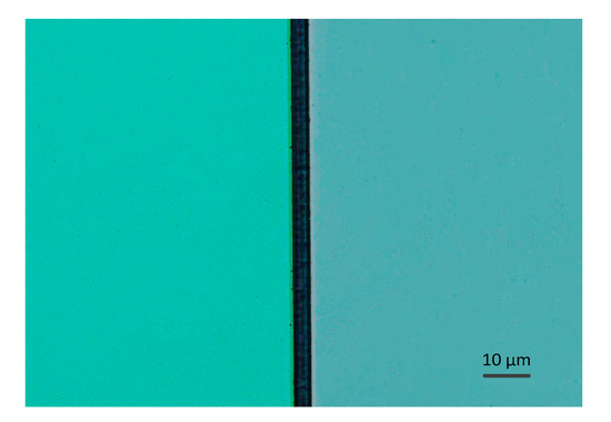
Figure 11.
The microscope photos of the joint width between bandpass filter for the region 3.55–3.75 µm and bandpass filter for the region 4.85–4.95 µm.
4.4. Infrared Spectroscopy Transmittance Test and the Error Analysis
The infrared transmittance spectra of the 3.55–3.75 and 4.85–4.95 µm films are shown in Figure 12. The spectra show that the average transmittance of both filters is above 83.5%. The FWHM of the two filters are 274 and 246 nm, respectively. The transmittance in the blocking area is less than 10−3 (OD3). However, the transmittance and the bandwidth decrease and the ripple increases compared with theoretical values. To find the reason, the cross-sectional SEM micrograph of 3.55–3.75 µm band filter for verification was conducted.
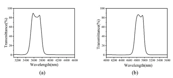
Figure 12.
Measured transmittance of (a) bandpass filter for the region 3.55–3.75 µm and (b) bandpass filter for the region 4.85–4.95 µm. Zinc sulfide (ZnS) and germanium (Ge) were the thin-film materials used.
A cross-sectional SEM micrograph of filter structure is displayed in Figure 13. The layers are very homogenous and the interfaces are smooth and abrupt. This is the reason that the in-body scattering and surface scattering can be neglected. The details of the thickness differences of each layer are shown in Table 2.
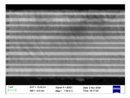
Figure 13.
Cross-sectional SEM micrograph of bandpass filter structure for the region 3.55–3.75 µm.
Table 2.
Comparison of the film thickness between the designed and the measured multilayered filter for 3.55–3.75 µm.
Figure 14 gives the comparison between the theoretical spectrum, simulated spectrum and measurement spectrum. Figure 14a gives theoretical spectrum of the filter. Figure 14b gives the simulated spectrum (simulated by applied actual thickness), Figure 14c gives the measured spectrum. The difference of Figure 14b,c is caused by the error of the measured thickness and the refractive index deviation during the deposition process. After analyzed, the thickness error is the reason of the degradations of peak transmission and bandwidth. In F-P structure, the spacer layers are the most sensitive when conducting pre-production sensitivity analysis.
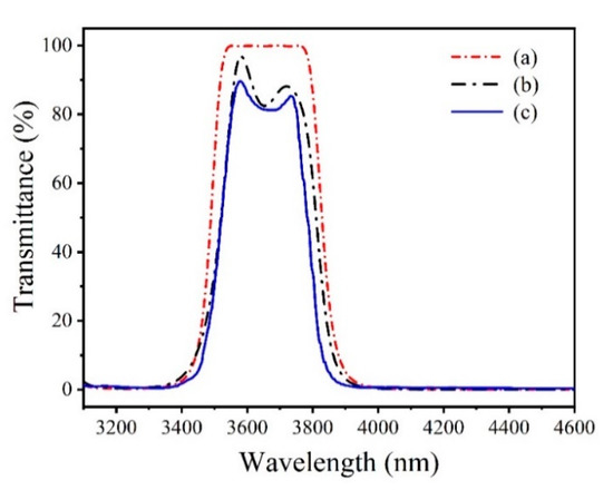
Figure 14.
Computed and measured transmittance of the filter for comparison. (a) Theoretical spectrum, (b) simulated spectrum (simulated by applied actual thickness), and (c) measured spectrum.
For further verification, two F-P filters were designed and shown in Figure 15a. Each filter consists of the same film structure HL 2H LH L HL 2H LH similar to our 3.55–3.75 µm filter structure, the reference wavelength is 3580nm, the thickness of space layer is 2H (optical thickness) for one filter and the thickness error of space layer was deliberately introduced for the other filter, the thickness of space layer is 1.9H (−5%),1.8H (−10%), respectively; the corresponding film structure is HL 1.9H LH L HL 1.9H LH, HL 1.8H LH L HL 1.8H LH, respectively. The peak transmission decreases from 91% to 55% and the bandwidth decreases from 208 to 136 nm.
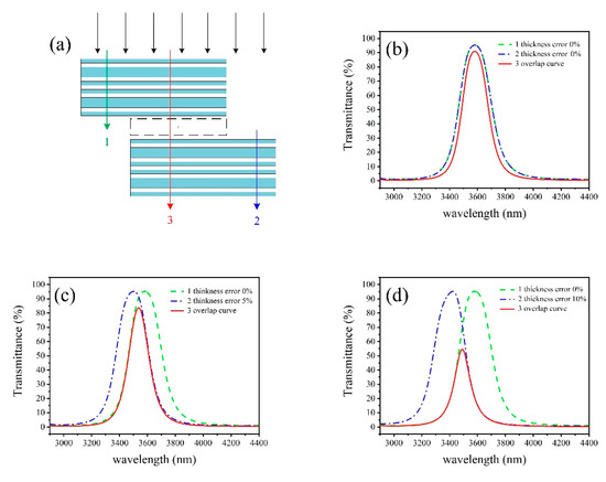
Figure 15.
(a) The schematic diagram of two designed filters with the same film structure HL2HLHLHL2HLH, the three calculated curves when one filter is HL 2H LH L HL 2H LH, the other filters are HL 2HLHLHL2HLH (b), HL1.9HLHLHL1.9HLH (c), HL1.8HLHLHL1.8HLH (d), respectively.
Figure 16 shows the simulated spectrum, when the designed thickness of spacer layers (layers 3, 9, 15, and 21) is in place of the actual thickness. Seen from the figure, the peak transmission and bandwidth increase and approach the optimized spectrum. Therefore, it can be confirmed that the deviation of the spacer layer is the main reason of the degradations of peak transmission and bandwidth. Figure 16d shows the simulated spectrum, where the designed thickness is now used in place of the actual thickness and the layer 1 and layer 4 in place of the designed thickness. As seen from the figure, the ripple decreases remarkably.
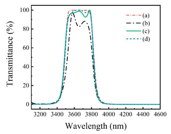
Figure 16.
Computed and measured transmittance of the F-P filter for comparison. (a) Theoretical spectrum, (b) simulated spectrum (simulated by applied actual thickness), (c) simulated spectrum (simulated by applied designed spacer layer thickness), and (d) simulated spectrum (based on c, further simulated by applied designed spacer layer and designed layer 1 and layer 4 thickness).
4.5. UV Radiation
As the filters will also be applicable for uses in space in future, testing for the UV radiation damage to the filters is also necessary. The filter was exposed to ultraviolet irradiation of 1500 equivalent sun hours (ESH) and tested. Figure 17 shows that the filter (sample) does not show degradation and demonstrated high anti-ultraviolet irradiation ability, in which there is no change in appearance and performance after 6 months exposure to ambient humidity.
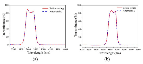
Figure 17.
Measured transmittance of (a) bandpass filter for the region 3.55–3.75 µm and (b) bandpass filter for the region 4.85–4.95 µm before and after UV irradiation. Zinc sulfide (ZnS) and germanium (Ge) were the thin-film materials used.
5. Conclusions
In this work, dual-channel bandpass thin-film filters for the mid-infrared were designed and fabricated by electron beam evaporation and lift-off process techniques. The thin-film filter consists of a 4-cavity F-P structure. The average transmittance of the filter is more than 83.5% in the passband and the cutoff is OD3 with a 4.5 µm joint width. The filter has a stronger anti-ultraviolet irradiation ability and long-term stability. The difference between measured transmittance and theoretical transmittance are caused by deposition thickness error. The deviation of the spacer layer is the main reason for the degradations of peak transmission and bandwidth. The results show that the dual filter has good spectral characteristics and has smaller joint width on the basis of thicker film thickness. The dual filter meets the requirements of integrated optical systems for space applications.
Author Contributions
Conceptualization, S.Z. and W.L.; methodology, F.G., Z.L., J.X. and C.W.; software, L.Z., S.Z. and F.G.; validation, K.Z., K.L., X.X. and S.S.; investigation, Z.L., S.Z., K.L. and F.G.; writing—original draft preparation, L.Z.; writing—review and editing, S.S. and S.Z. All authors have read and agreed to the published version of the manuscript.
Funding
This work was funded by the Key Laboratory for Equipment Pre-research (No. 6142207190407) and the Scientific Research Program of Shaanxi Provincial Education Department (No.21JY017).
Institutional Review Board Statement
Not applicable.
Informed Consent Statement
Not applicable.
Data Availability Statement
The data presented in this study are available on request from the corresponding author.
Conflicts of Interest
The authors declare no conflict of interest.
References
- Krause, F.; Betz, H.; Lysobey, D. Pollution detection by digital correlation of multispectral, stereo-image pairs. Atmos. Environ. 1973, 7, 455–476. [Google Scholar] [CrossRef]
- Sader, S.A. Analysis of effective radiant temperatures in a pacific northwest forest using thermal infrared multispectral scanner data. Remote Sens. Environ. 1986, 19, 105–115. [Google Scholar] [CrossRef]
- Calvini, R.; Ulrici, A.; Amigo, J.M. Growing applications of hyperspectral and multispectral imaging. In Data Handling in Science and Technology; Elsevier BV: Amsterdam, The Netherlands, 2020; Volume 32, pp. 605–629. [Google Scholar]
- Wang, D.; Li, D.; Fan, D.; Wang, J.; Dong, M.; Fang, D. Development status of space spectral imaging and integrated optical thin film technology. Vac. Cryog. 2019, 25. [Google Scholar] [CrossRef]
- Yi, D.; Kong, L. Fabrication of densely patterned micro-arrayed multichannel optical filter mosaic. J. Micro Nanolithography MEMS MOEMS 2011, 10, 33020. [Google Scholar] [CrossRef]
- Jaing, C.-C.; Yang, C.-R.; Chang, C.-M.; Chang, Y.-H.; Lee, C.-T.; Hsiao, C.-N. Miniaturized Multilayer Dielectric Coatings Using Metal Masks Fabricated by Electroforming and Photolithography Technologies; SPIE: San Diego, CA, USA, 2008; Volume 7067. [Google Scholar]
- Wang, S.; Wang, L.; Wu, Y.; Wang, Z.; Liu, D.; Lin, B.; Chen, X.; Lu, W. Arrays of narrow bandpass filters fabricated by combinatorial etching technique. Acta Opt. Sin. 2006, 26, 746–751. [Google Scholar]
- Kutteruf, M.R.; Yetzbacher, M.K.; DePrenger, M.J.; Novak, K.M.; Miller, C.A.; Kanaev, A. 9-band SWIR multispectral sensor providing full-motion video. SPIE Def. Secur. 2014, 9076, 90760. [Google Scholar] [CrossRef]
- Pan, Y.; Chen, J. Design and fabrication of microstructure narrowband filter. J. Appl. Opt. 2017, 38, 78–82. [Google Scholar]
- Yi, D.; Kong, L.; Wang, J.; Zhao, F. Fabrication of multispectral imaging technology driven MEMS-based micro-arrayed multichannel optical filter mosaic. Adv. Fabr. Technol. Micro Nano Opt. Photonics IV 2011, 7927, 792711. [Google Scholar]
- Duan, Y.; Cai, C.; Liang, H.; Jia, T.; Yin, S. Design and preparation of a 6-channel fan-shaped integrated narrow-band filter in the mid-infrared band. Coatings 2019, 9, 567. [Google Scholar] [CrossRef] [Green Version]
- Kong, L.; Yi, D.; Sprigle, S.H.; Wang, F.; Wang, C.; Liu, F.; Adibi, A.; Tummala, R. Single sensor that outputs narrowband multispectral images. J. Biomed. Opt. 2010, 15, 010502. [Google Scholar] [CrossRef] [PubMed] [Green Version]
- He, X.; Jie, J.; Yang, J.; Han, Y.; Zhang, S. A mid-infrared dual-band filter with ultra-high resolving power. IEEE Photon. J. 2020, 12. [Google Scholar] [CrossRef]
- Kischkat, J.; Peters, S.; Semtsiv, M.P.; Wegner, T.; Elagin, M.; Monastyrskyi, G.; Flores, Y.V.; Kurlov, S.; Masselink, W.T. Ultra-narrow angle-tunable Fabry–Perot bandpass interference filter for use as tuning element in infrared lasers. Infrared Phys. Technol. 2014, 67, 432–435. [Google Scholar] [CrossRef]
- Macleod, H.A. Thin-Film Optical Filters; IoP, Bristol and Philadelphia: Bristol, UK, 2001. [Google Scholar]
- Tang, J.F.G.; Liu, X.; Li, H.F. Modern Optical Thin Film Technology; Zhejiang University Press: Hangzhou, China, 2006. [Google Scholar]
Publisher’s Note: MDPI stays neutral with regard to jurisdictional claims in published maps and institutional affiliations. |
© 2021 by the authors. Licensee MDPI, Basel, Switzerland. This article is an open access article distributed under the terms and conditions of the Creative Commons Attribution (CC BY) license (https://creativecommons.org/licenses/by/4.0/).