
Modeling and Experimental Investigations of Nanostructured Ag Thin Films Produced by Oblique-Angle Deposition and Its SERS Performance

 ,
,
Abstract
1. Introduction
2. Background of Simulation
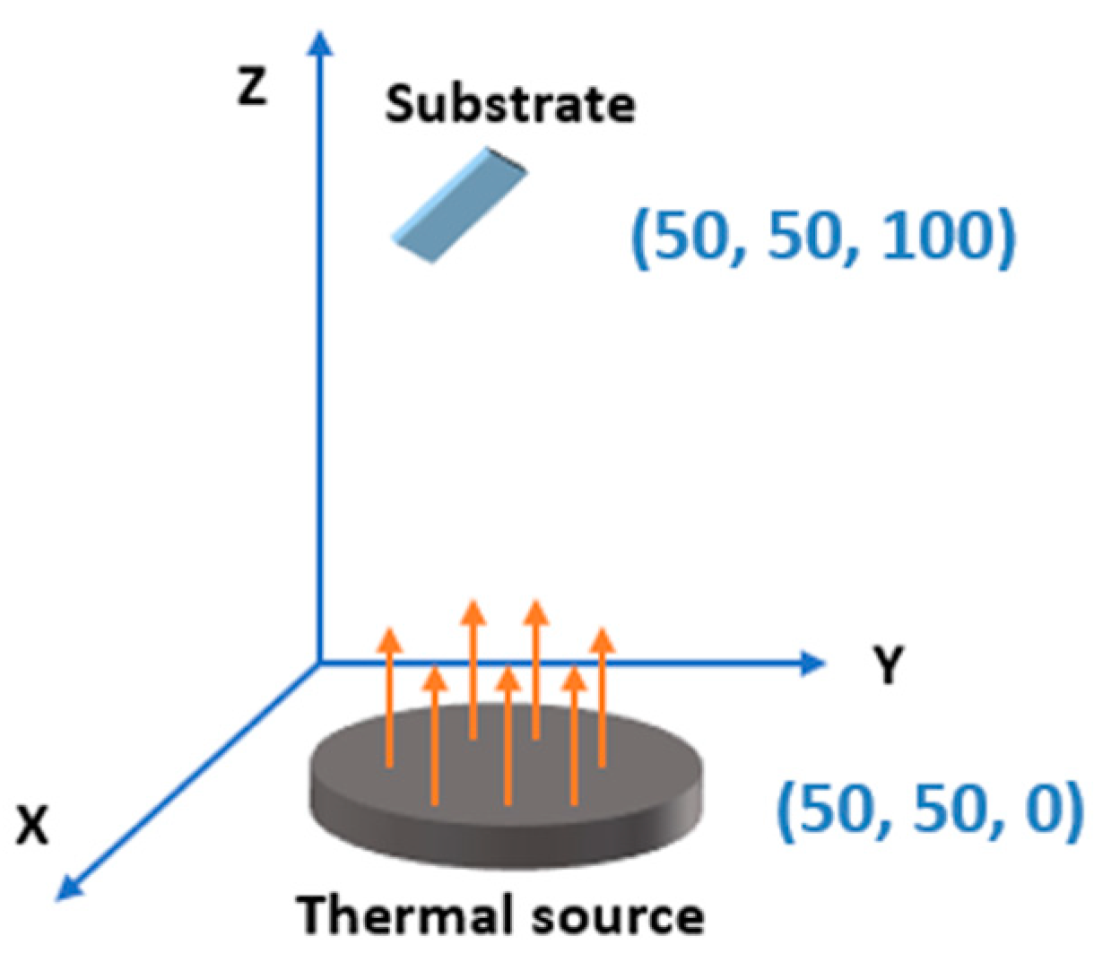
2.1. Nanostructure Simulation Using the KMC Method
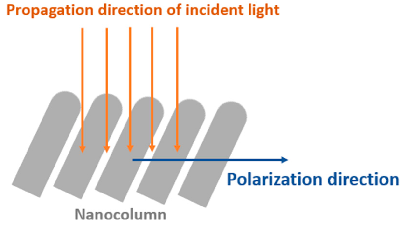
2.2. SERS Performance Simulation Model
3. Experiment
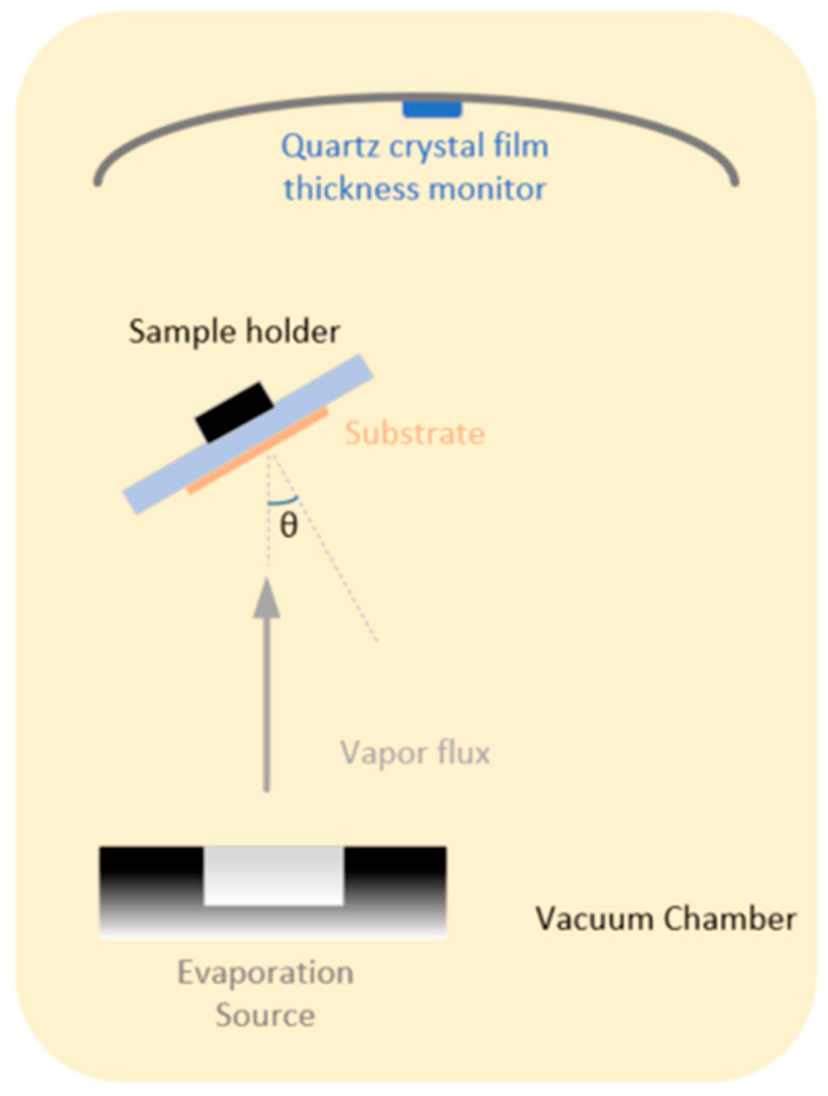
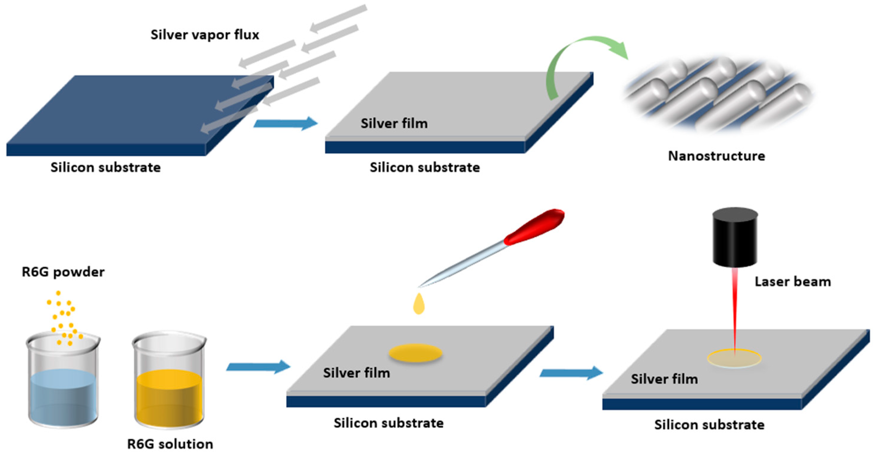
3.1. Deposition
3.2. Characterization
4. Results and Discussions
4.1. Comparison of KMC Simulation and Experimental Result
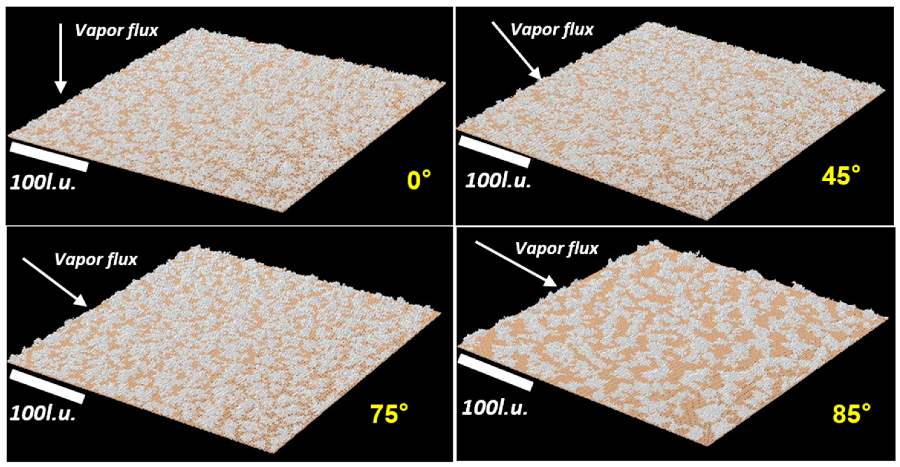
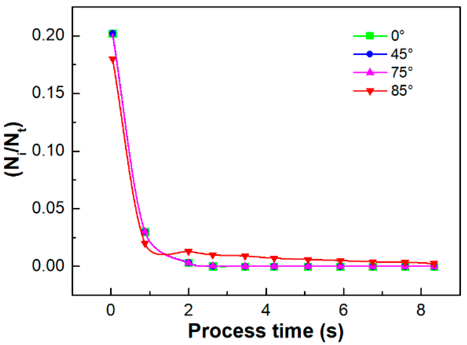
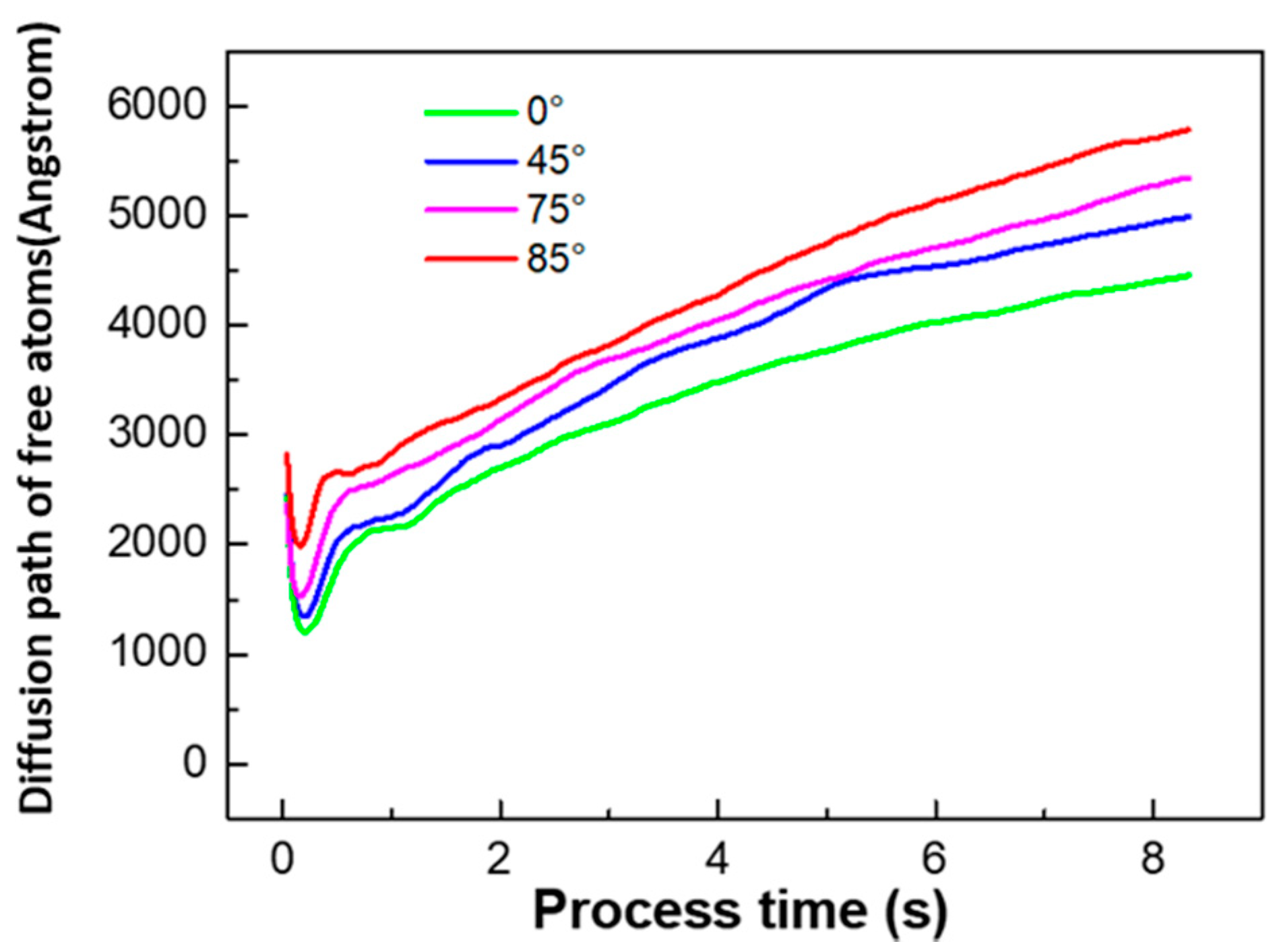
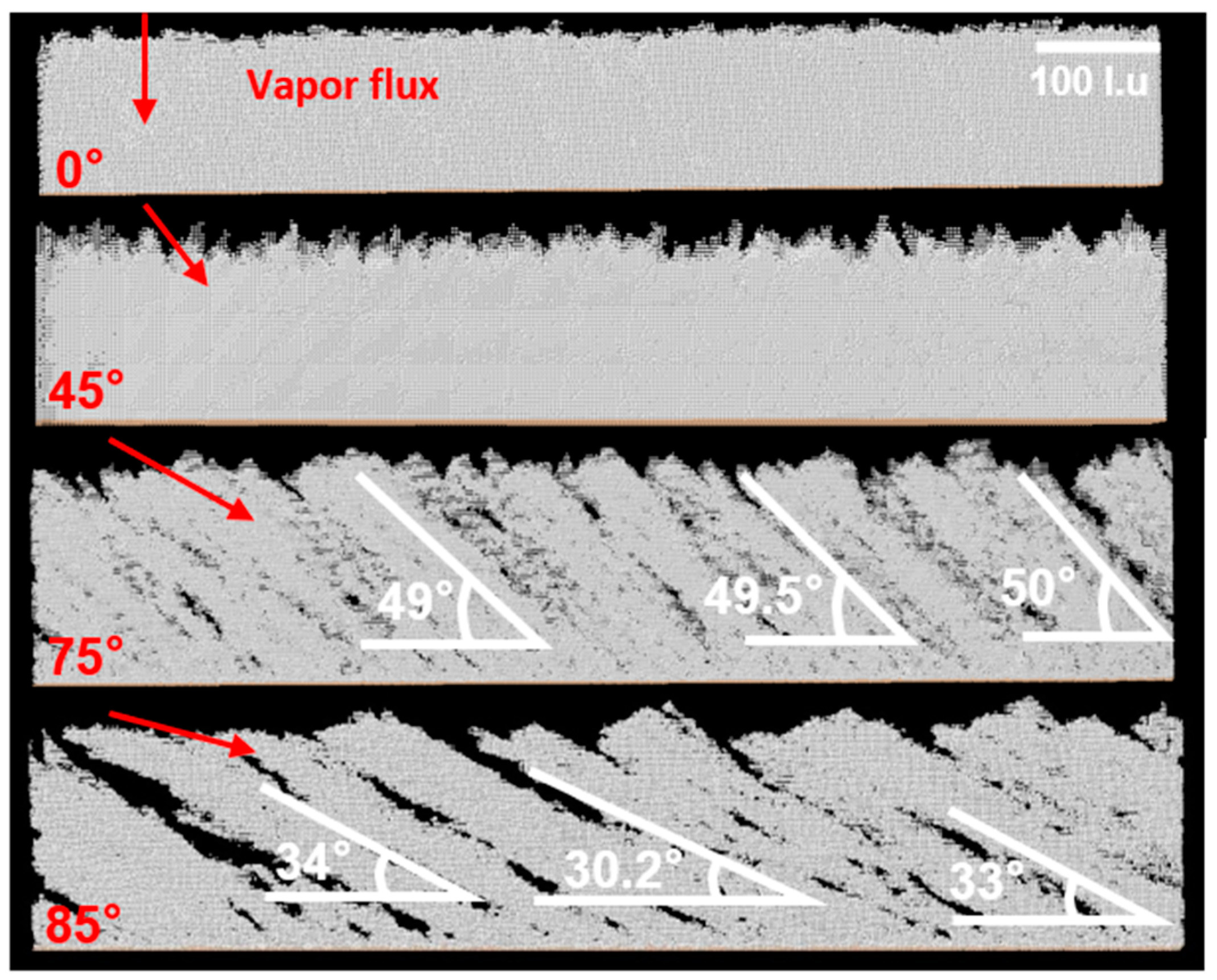
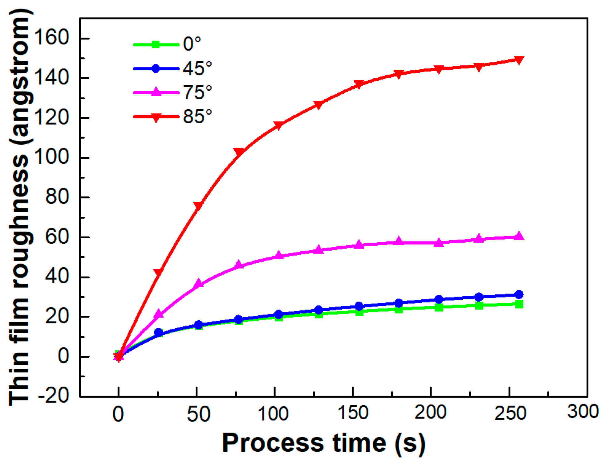
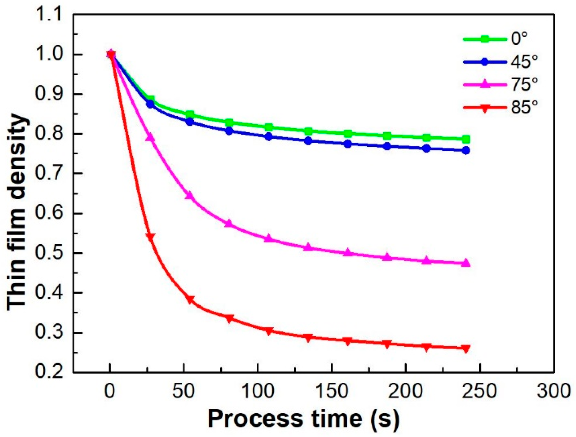
4.1.1. KMC Simulation Results
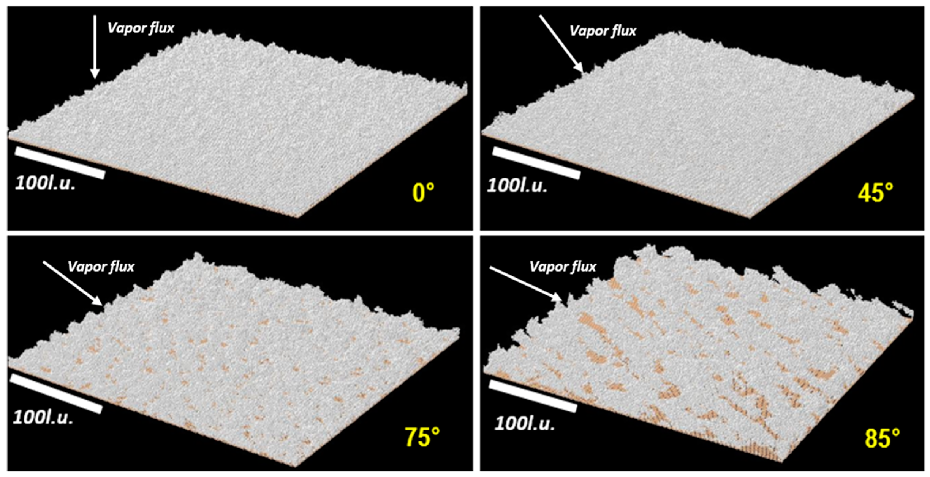
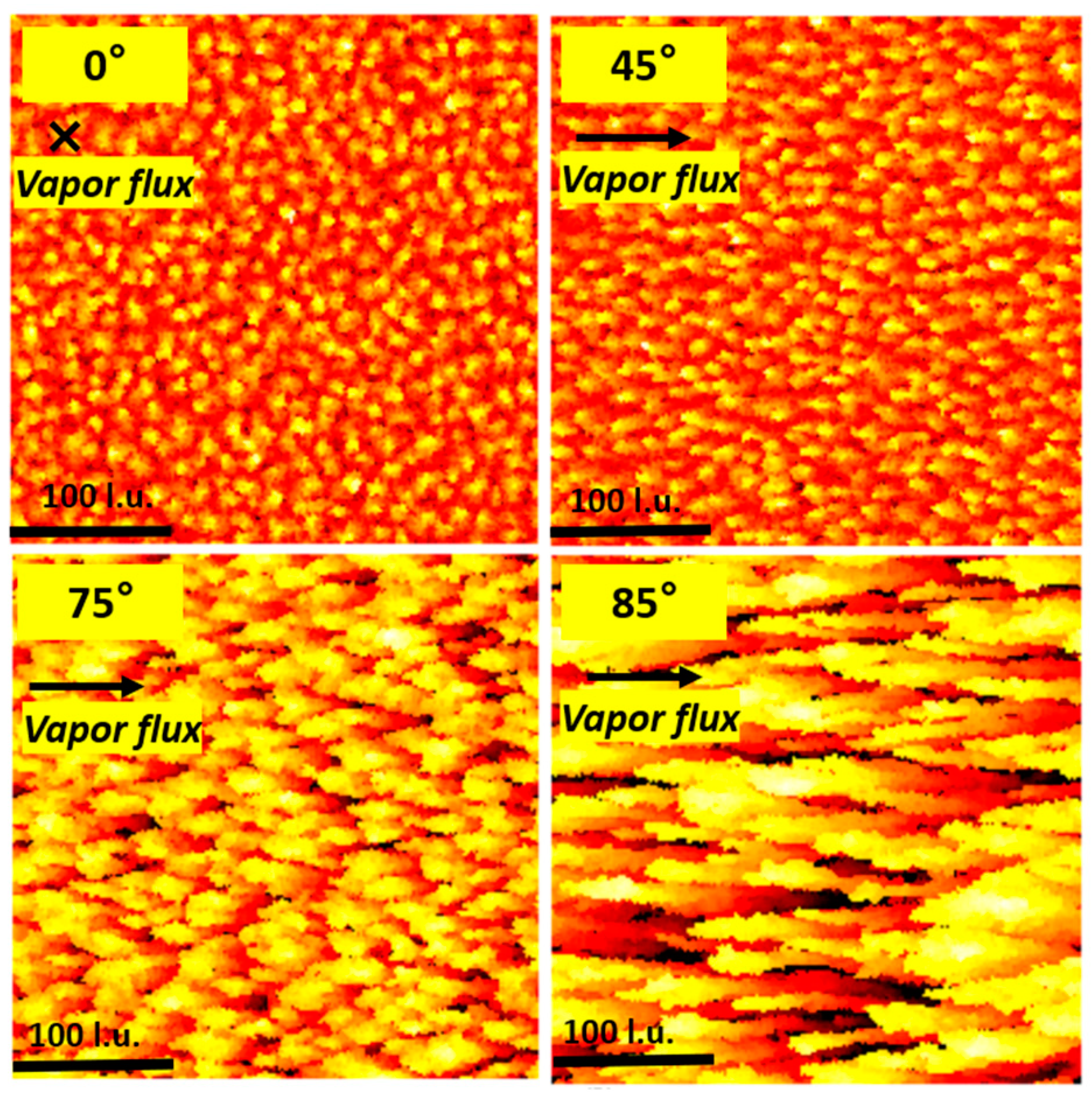
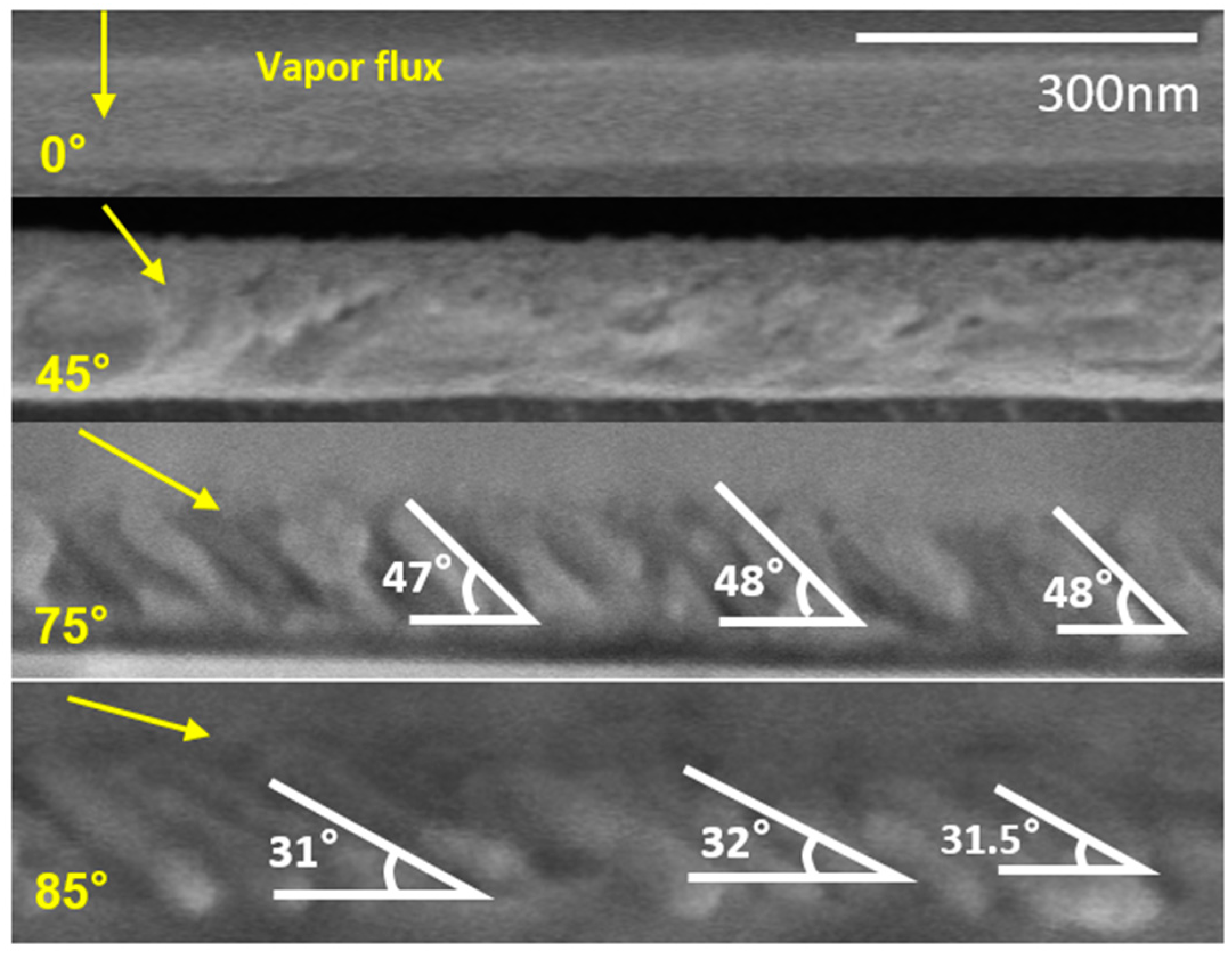
4.1.2. Experimental Results
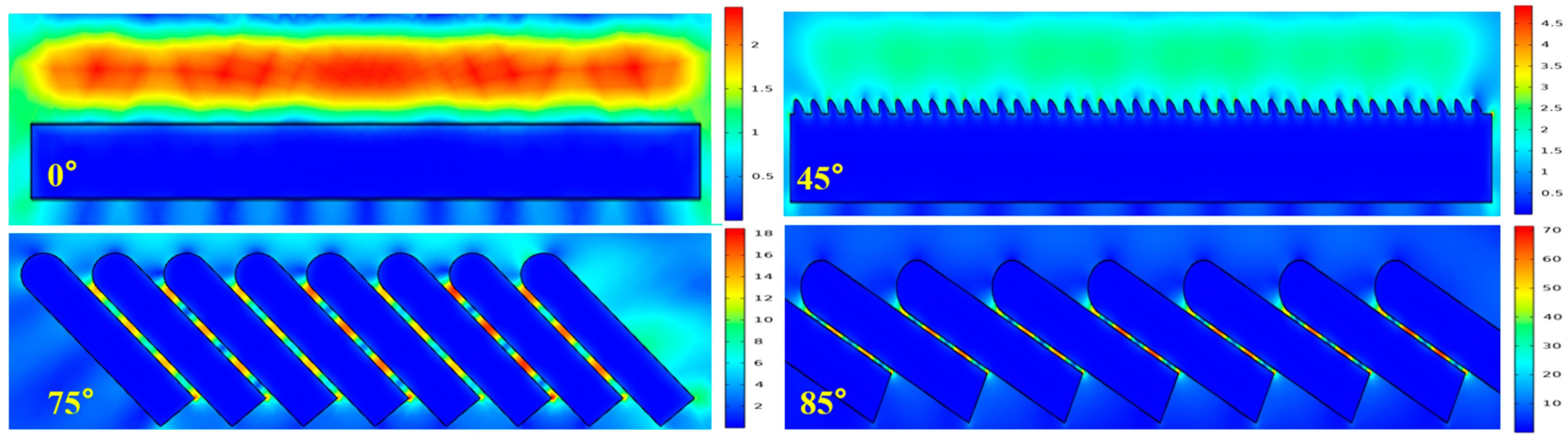
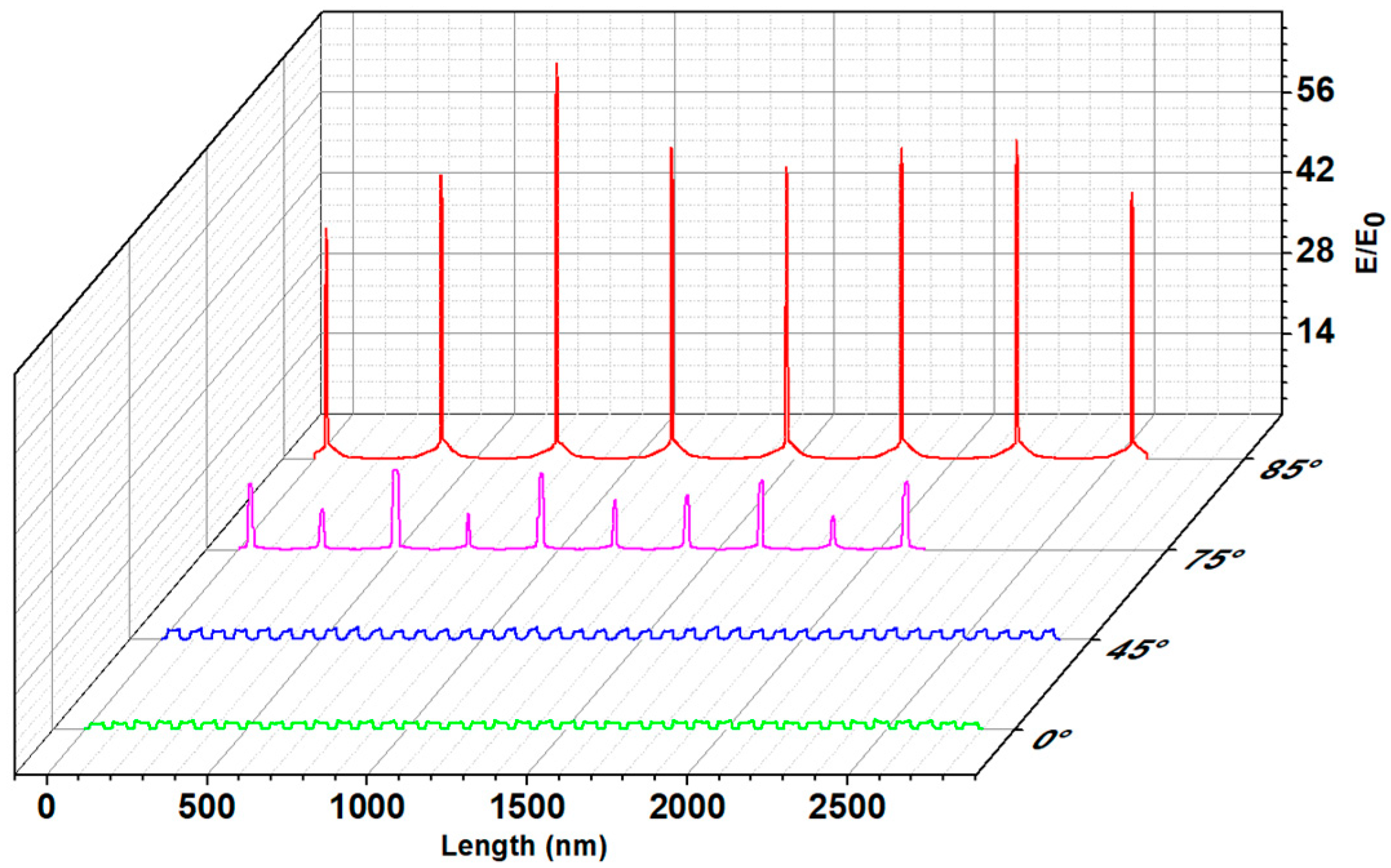
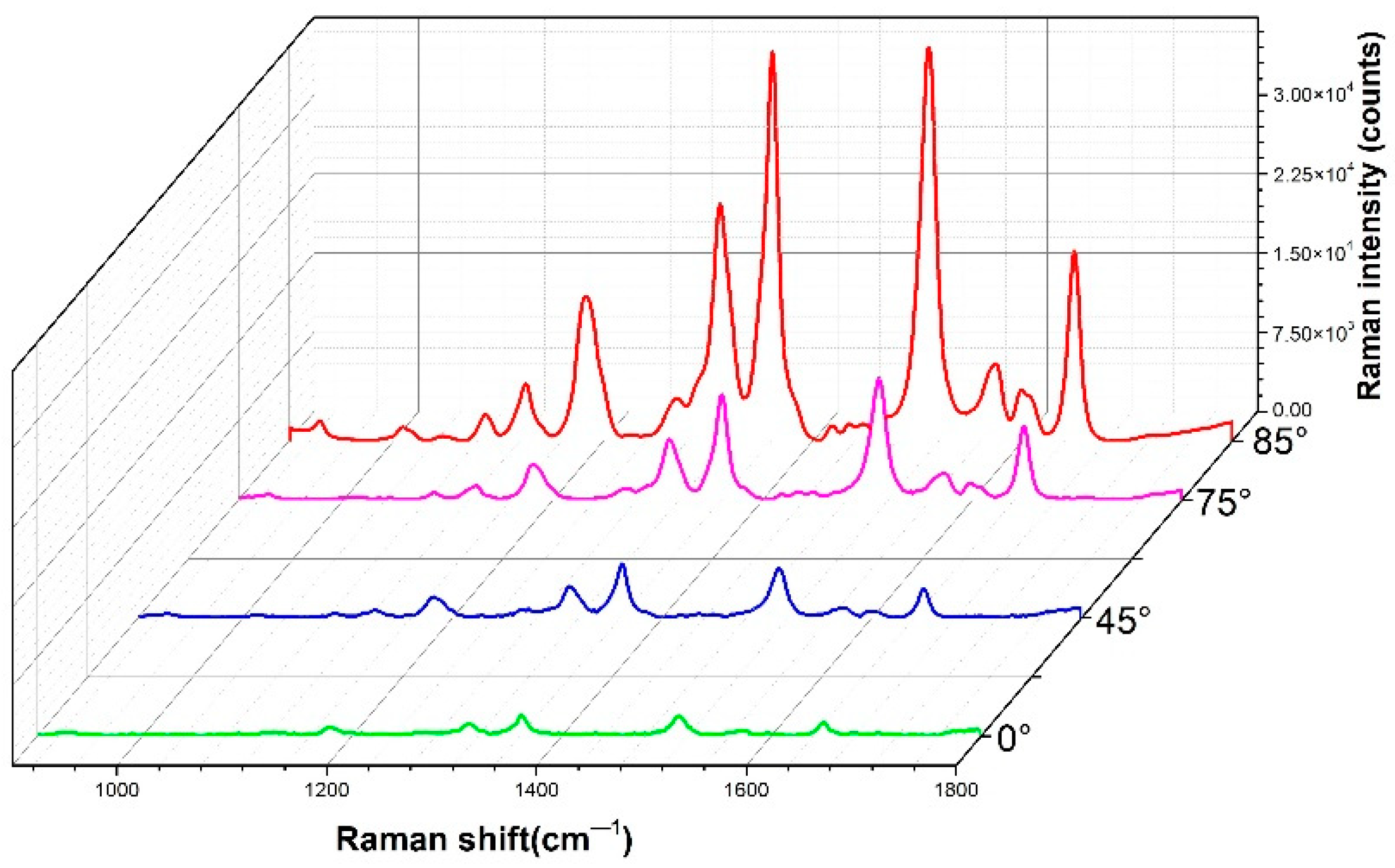
4.2. Comparison of SERS Performance Simulation Results and Experimental Results
5. Conclusions
Author Contributions
Funding
Institutional Review Board Statement
Informed Consent Statement
Data Availability Statement
Acknowledgments
Conflicts of Interest
References
- Hawkeye, M.M.; Taschuk, M.T.; Brett, M.J. Glancing Angle Deposition of Thin Films: Engineering the Nanoscale; John Wiley & Sons: Hoboken, NJ, USA, 2014. [Google Scholar]
- Song, S.; Keating, M.; Chen, Y.; Placido, F. Reflectance and surface enhanced Raman scattering (SERS) of sculptured silver films deposited at various vapor incident angles. Meas. Sci. Technol. 2012, 23, 084007. [Google Scholar] [CrossRef]
- Keating, M.; Song, S.; Wei, G.; Graham, D.; Chen, Y.; Placido, F. Ordered Silver and Copper Nanorod Arrays for Enhanced Raman Scattering Created via Guided Oblique Angle Deposition on Polymer. J. Phys. Chem. 2014, 118, 4878–4884. [Google Scholar] [CrossRef]
- Chaney, S.B.; Shanmukh, S.; Dluhy, R.A.; Zhao, Y.P. Aligned silver nanorod arrays produce high sensitivity surface-enhanced Raman spectroscopy substrates. Appl. Phys. Lett. 2005, 87, 031908. [Google Scholar] [CrossRef]
- Karunasiri, R.P.U.; Bruinsma, R.; Rudnick, J. Thin-film growth and the shadowing instability. Phys. Rev. Lett. 1989, 62, 788–791. [Google Scholar] [CrossRef]
- Driskell, J.D.; Zhu, Y.; Kirkwood, C.D.; Zhao, Y.; Dluhy, R.A.; Tripp, R.A. Rapid and Sensitive Detection of Rotavirus Molecular Signatures Using Surface Enhanced Raman Spectroscopy. PLoS ONE 2010, 5, e10222. [Google Scholar] [CrossRef]
- Hennigan, S.L.; Driskell, J.D.; Dluhy, R.A.; Zhao, Y.; Tripp, R.A.; Waites, K.B.; Krause, D.C. Detection of Mycoplasma pneumoniae in Simulated and True Clinical Throat Swab Specimens by Nanorod Array-Surface-Enhanced Raman Spectroscopy. PLoS ONE 2010, 5, e13633. [Google Scholar] [CrossRef]
- Wu, X.; Gao, S.; Wang, J.-S.; Wang, H.; Huang, Y.-W.; Zhao, Y. The surface-enhanced Raman spectra of aflatoxins: Spectral analysis, density functional theory calculation, detection and differentiation. Analyst 2012, 137, 4226–4234. [Google Scholar] [CrossRef] [PubMed]
- Zhu, Y.; Dluhy, R.A.; Zhao, Y. Development of silver nanorod array based fiber optic probes for SERS detection. Sens. Actuators B Chem. 2011, 157, 42–50. [Google Scholar] [CrossRef]
- Chen, J.; Abell, J.; Huang, Y.-W.; Zhao, Y. On-Chip Ultra-Thin Layer Chromatography and Surface Enhanced Raman Spectroscopy. Lab Chip 2012, 12, 3096–3102. [Google Scholar] [CrossRef]
- Moskovits, M. Surface-enhanced Raman spectroscopy: A brief retrospective. J. Raman Spectrosc. 2005, 36, 485–496. [Google Scholar] [CrossRef]
- NASCAM. Available online: http://www.unamur.be/sciences/physique/pmr/telechargement/logiciels/nascam (accessed on 15 January 2021).
- Claassens, C.H.; Hoffman, M.J.H.; Terblans, J.J.; Swart, H.C. Kinetic Monte Carlo Simulation of the Growth of Various Nanostructures through Atomic and Cluster Deposition: Application to Gold Nanostructure Growth on Graphite. J. Phys. Conf. Ser. 2006, 29, 185–189. [Google Scholar] [CrossRef]
- Tan, X.; Zhou, Y.; Zheng, X. Dependence of morphology of pulsed-laser deposited coatings on temperature: A kinetic Monte Carlo simulation. Surf. Coat. Technol. 2005, 197, 288–293. [Google Scholar] [CrossRef]
- Trushin, O.; Karim, A.; Kara, A.; Rahman, T.S. Self-learning kinetic Monte Carlo method: Application to Cu (111). Phys. Rev. B 2005, 72. [Google Scholar] [CrossRef]
- Ohring, M. Materials Science of Thin Films; Academic Press: Cambridge, MA, USA, 2001. [Google Scholar]
- Lucas, S.; Moskovkin, P. Simulation at high temperature of atomic deposition, islands coalescence, ostwald and inverse ostwald ripening with a general simple kinetic monte carlo code. Thin Solid Film. 2010, 518, 5355–5361. [Google Scholar] [CrossRef]
- De Miguel, J.J.; Sanchez, A.; Cebollada, A.; Gallego, J.M.; Ferron, J.; Ferrer, S. The surface morphology of a growing crystal studied by thermal energy atom scattering (TEAS). Surf. Sci. 1987, 189, 1062–1068. [Google Scholar] [CrossRef]
- Antczak, G.; Ehrlich, G. Surface Diffusion: Metals, Metal Atoms, and Clusters; Cambridge University Press: Cambridge, UK, 2010; pp. 295–300. [Google Scholar]
- Askill, J. Tracer Diffusion Data for Metals, Alloys, and Simple Oxides; Springer: New York, NY, USA, 1970. [Google Scholar]
- Dervaux, J.; Cormier, P.-A.; Moskovkin, P.; Douheret, O.; Konstantinidis, S.; Lazzaroni, R.; Lucas, S.; Snyders, R. Synthesis of nanostructured Ti thin films by combining glancing angle deposition and magnetron sputtering: A joint experimental and modeling study. Thin Solid Film. 2017, 636, 644–657. [Google Scholar] [CrossRef]
- Parthasarathy, H. Waves and Optics; CRC Press: London, UK, 2021. [Google Scholar]
- Kneipp, K. Surface-enhanced Raman scattering. Phys. Today 2007, 11, 40–46. [Google Scholar] [CrossRef]
- Tait, R.N.; Smy, T.; Brett, M.J. Modelling and characterization of columnar growth in evaporated films. Thin Solid Film. 1993, 226, 196–201. [Google Scholar] [CrossRef]
- Hin, O.M.C. Metal Nanostructures Made by Oblique Angle Deposition on Templates for Solid State Surface Enhanced Raman Spectroscopy Substrates. Ph.D. Thesis, University of the West of Scotland, Glasgow, UK, 2019. [Google Scholar]
- Alvarez, R.; Garcia-Martin, J.M.; Macias-Montero, M.; Gonzalez-Garcia, L.; González, J.C.; Rico, V.J.; Perlich, J.; Cotrino, J.; González-Elipe, A.R.; Palmero, A. Growth regimes of porous gold thin films deposited by magnetron sputtering at oblique incidence: From compact to columnar microstructures. Nanotechnology 2013, 24, 45604. [Google Scholar] [CrossRef]
- Dalla Torre, J.; Gilmer, G.H.; Windt, D.L.; Kalyanaraman, R.; Baumann, F.H.; O’Sullivan, P.L.; Sapjeta, J.; Díaz de la Rubia, T.; Djafari Rouhani, M. Microstructure of thin films sputtered onto inclined substrates: Experiments and atomistic simulations. J. Appl. Phys. 2003, 94, 263–271. [Google Scholar] [CrossRef]
- Rico, V.J.; Borrás, A.; Yubero, F.; Espinos, J.P.; Frutos, F.; González-Elipe, A.R. Wetting Angles on Illuminated Ta2O5 Thin Films with Controlled Nanostructure. J. Phys. Chem. C 2009, 113, 3775–3784. [Google Scholar] [CrossRef]


| Parameters and Physical Constant | Value |
|---|---|
| Free diffusion (Ea_diff) | 0.5 ev |
| Hops with an increase or decrease of neighboring atoms number (Ea_nn_inc/Ea_nn_dec) | 1.9 ev |
| Hop down or up from one level to another (Ea_up/Ea_down) | 2.0 ev |
| Detachment from an island or substrate feature (Ea_detach) | 1.95 ev |
| Evaporation from the substrate or layers (Ea_evap) | 4.5 ev |
| Substrate temperature | 323 k |
| Substrate bind energy | 3.52 ev |
| Deposition Parameters | Value |
|---|---|
| Thin-film binding energy | 2.97 ev |
| Incident energy of an atom | 0.6 ev |
| Deposition angle | 0°/45°/75°/85° |
| Deposition rate | 0.3 mL/s |
| Deposition Angle | Simulation(Average) | Experiment(Average) | Theoretical Estimation |
|---|---|---|---|
| 75° | 49.1° | 47.4° | 40° |
| 85° | 32.8° | 31.8° | 33° |
| Deposition Angle | Thin-Film Surface Roughness (Simulation) | Estimation from Simulation (nm) | Thin-Film Surface Roughness (Experiment) |
|---|---|---|---|
| 0° | 6.5 l.u | 2.6 nm | 1.8 nm |
| 45° | 7.6 l.u | 3.1 nm | 2.1 nm |
| 75° | 14.7 l.u | 6.0 nm | 6.7 nm |
| 85° | 36.6 l.u | 14.9 nm | 18 nm |
Publisher’s Note: MDPI stays neutral with regard to jurisdictional claims in published maps and institutional affiliations. |
© 2021 by the authors. Licensee MDPI, Basel, Switzerland. This article is an open access article distributed under the terms and conditions of the Creative Commons Attribution (CC BY) license (https://creativecommons.org/licenses/by/4.0/).
Share and Cite
Hui, D.; Zhou, S.; Cai, C.; Song, S.; Wu, Z.; Song, J.; Zhang, D.; Meng, X.; Lu, B.; Duan, Y.; et al. Modeling and Experimental Investigations of Nanostructured Ag Thin Films Produced by Oblique-Angle Deposition and Its SERS Performance. Coatings 2021, 11, 458. https://doi.org/10.3390/coatings11040458
Hui D, Zhou S, Cai C, Song S, Wu Z, Song J, Zhang D, Meng X, Lu B, Duan Y, et al. Modeling and Experimental Investigations of Nanostructured Ag Thin Films Produced by Oblique-Angle Deposition and Its SERS Performance. Coatings. 2021; 11(4):458. https://doi.org/10.3390/coatings11040458
Chicago/Turabian StyleHui, Datai, Shun Zhou, Changlong Cai, Shigeng Song, Zhentao Wu, Jian Song, Da Zhang, Xiao Meng, Bo Lu, Yingbu Duan, and et al. 2021. "Modeling and Experimental Investigations of Nanostructured Ag Thin Films Produced by Oblique-Angle Deposition and Its SERS Performance" Coatings 11, no. 4: 458. https://doi.org/10.3390/coatings11040458
APA StyleHui, D., Zhou, S., Cai, C., Song, S., Wu, Z., Song, J., Zhang, D., Meng, X., Lu, B., Duan, Y., Tursun, H., & Gibson, D. (2021). Modeling and Experimental Investigations of Nanostructured Ag Thin Films Produced by Oblique-Angle Deposition and Its SERS Performance. Coatings, 11(4), 458. https://doi.org/10.3390/coatings11040458