Article

Epitaxial Growth and Stoichiometry Control of Ultrawide Bandgap ZnGa2O4 Films by Pulsed Laser Deposition

1
School of Material Science and Engineering, Kunming University of Science and Technology, Kunming 650093, China
2
Ningbo Institute of Material Technology and Engineering, Chinese Academy of Sciences, Ningbo 315201, China
*
Authors to whom correspondence should be addressed.
Coatings 2021, 11(7), 782; https://doi.org/10.3390/coatings11070782
Submission received: 7 June 2021 / Revised: 28 June 2021 / Accepted: 28 June 2021 / Published: 30 June 2021
(This article belongs to the Special Issue Nanocomposite Thin Film and Multilayers)

Abstract

:
ZnGa2O4 is a promising semiconductor for developing high-performance deep-ultraviolet photodetectors owing to a number of advantageous fundamental characteristics. However, Zn volatilization during the ZnGa2O4 growth is a widely recognized problem that seriously degrades the film quality and the device performance. In this study, we report the synthesis of epitaxial ZnGa2O4 thin films by pulsed laser deposition using a non-stoichiometric Zn1+xGa2O4 target. It is found that supplementing excessive Zn concentration from the target is highly effective to stabilize stochiometric ZnGa2O4 thin films during the PLD growth. The influence of various growth parameters on the phase formation, crystallinity and surface morphology is systematically investigated. The film growth behavior further impacts the resulting optical absorption and thermal conductivity. The optimized epitaxial ZnGa2O4 film exhibits a full width at half maximum value of 0.6 degree for a 120 nm thickness, a surface roughness of 0.223 nm, a band gap of 4.79 eV and a room-temperature thermal conductivity of 40.137 W/(m⋅K). This study provides insights into synthesizing epitaxial ZnGa2O4 films for high performance optoelectronic devices.

1. Introduction

Deep-ultraviolet photodetectors (DUV PDs) with the characteristic spectral response in the range of 200–280 nm [1] have attracted significant research interests owing to their broad applications including optical communication, missile detection, environmental monitoring, and biochemical analysis [2,3,4,5,6]. Development of advanced DUV PD techniques applies strict requirements on the device responsivity, the response time, device weight and reliability. This becomes challenging for conventional DUV PDs including silicon-based PDs and photomultiplier tubes, which require to integrate additional UV filters and are more vulnerable to thermal and radiation damage [7]. As an alternative solution, wide bandgap semiconductors are promising candidates to address these challenges owing to their fundamental optical and electrical characteristics, such as inherent wide bandgap (Eg > 4.0 eV), tunable transport properties, superior thermal stability and radiation tolerance. Representative wide bandgap semiconductors include Ga2O3 [8], ZnGa2O4 (ZGO) [9,10,11,12,13], MgxZn1-xO [14,15], and AlxGa1-xN [16,17]. Significant research efforts have been devoted to developing efficient DUV PDs based on Ga2O3 and other semiconductors. A well-recognized challenging issue is the impurity phase segregation due to the stoichiometry modification or metastable phase formation [2,18].
Among these candidates, ZGO presents appealing advantages in fabricating high-performance DUV PDs, including the simple cubic structure, wide bandgap (4.6–5.2 eV) and large electron mobility (~100 cm2V−1s−1) [9,19]. To explore the full potential of ZGO in DUV PDs, a key prerequisite is to achieve the high-quality material growth. In particular, epitaxial ZGO film is highly desired due to its simplified nature for device integration. A number of methods have been adopted for growing ZGO films, which include sol-gel method [20], metal organic chemical vapor deposition (MOCVD) [13], radio frequency magnetron sputtering (RF) [10,21], and pulsed laser deposition (PLD) [22,23]. However, it is widely recognized Zn volatilization typically occurs during the ZGO film growth due to the much higher vapor pressure of Zn than that of Ga [9]. This problem could lead to a significant amount of non-stoichiometry defects and impurity phases that seriously degrades the film quality.
Epitaxial growth of ZGO film requires precise control of film stoichiometry, crystallinity and the growth rate. Compared to solution-based or chemical vapor phase synthesis methods, the PLD technique is well-suite for the above requirements, as it enables more convenient adjustment of the Zn/Ga ratio and atomic-level control of adatom arrival rate during the film growth [24,25]. Yia et al. showed that Zn-deficient ZGO films with Zn/Ga less than 0.38 were obtained by PLD from a stoichiometric ZnGa2O4 target, reflecting the Zn loss process during PLD growth (Figure 1a) [26]. To compensate the Zn loss during growth, a major strategy is to improve the Zn concentration in the laser ablated target. This was achieved by preparing mosaic targets with a partial ZnO target embedded in a major ZGO target [27,28], or by alternatively ablating single-phase ZGO and single-phase ZnO targets during growth [29].
While previous efforts demonstrate that the stochiometric control is critical to stabilize epitaxial, phase-pure ZGO films, the fundamental understanding of the relation between stoichiometry and the film growth behavior is not fully explored. In this study, we develop an effective strategy of growing epitaxial ZGO films by PLD using a non-stoichiometric Zn1+xGa2O4 (x = 6.5) target with excessive Zn concentration. This is in sharp contrast to the film deposited from a stochiometric Zn1+xGa2O4 target (x = 0), which consists of Ga2O3 impurity phase due to Zn volatilization (Figure 1b). Using the non-stoichiometric singe-target approach, we systematically study the effects of target Zn/Ga ratio, growth temperature, oxygen pressure and laser fluence on the phase composition, surface morphology, optical properties and thermal conductivity.

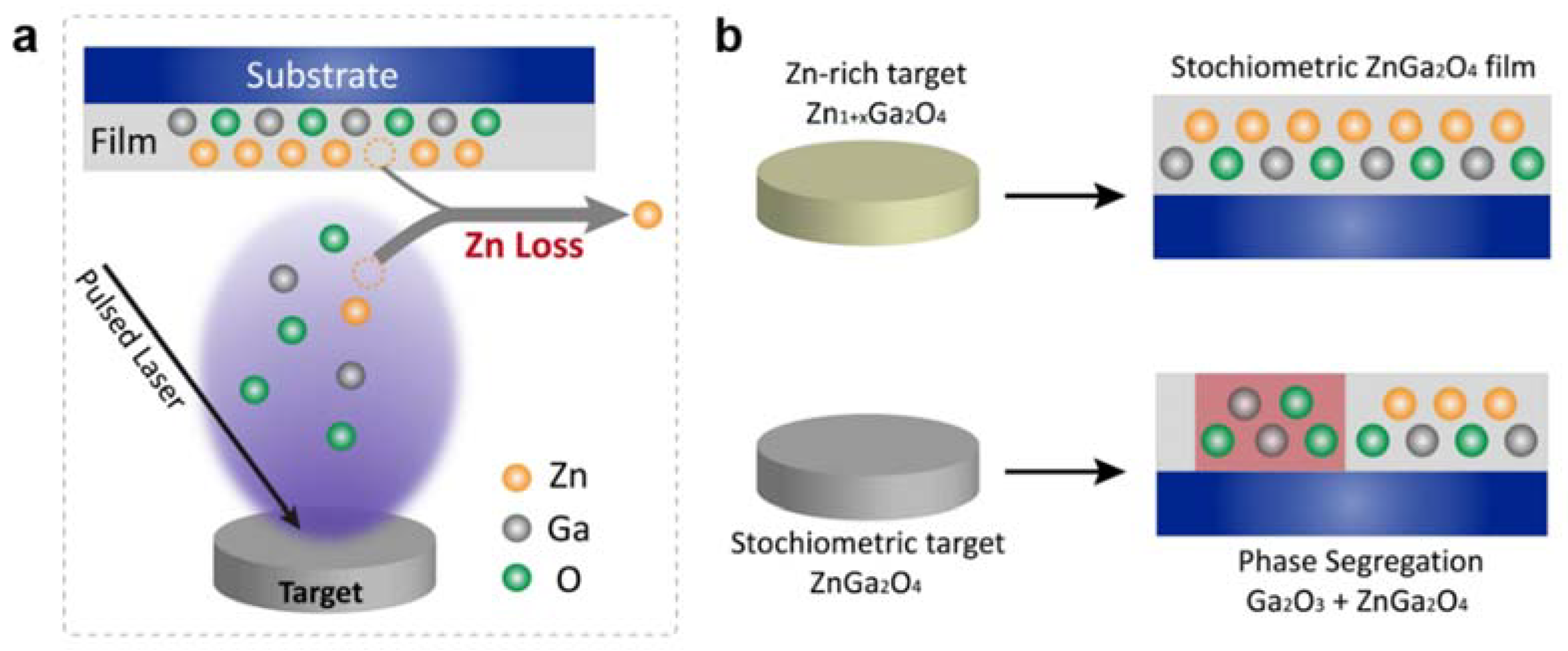
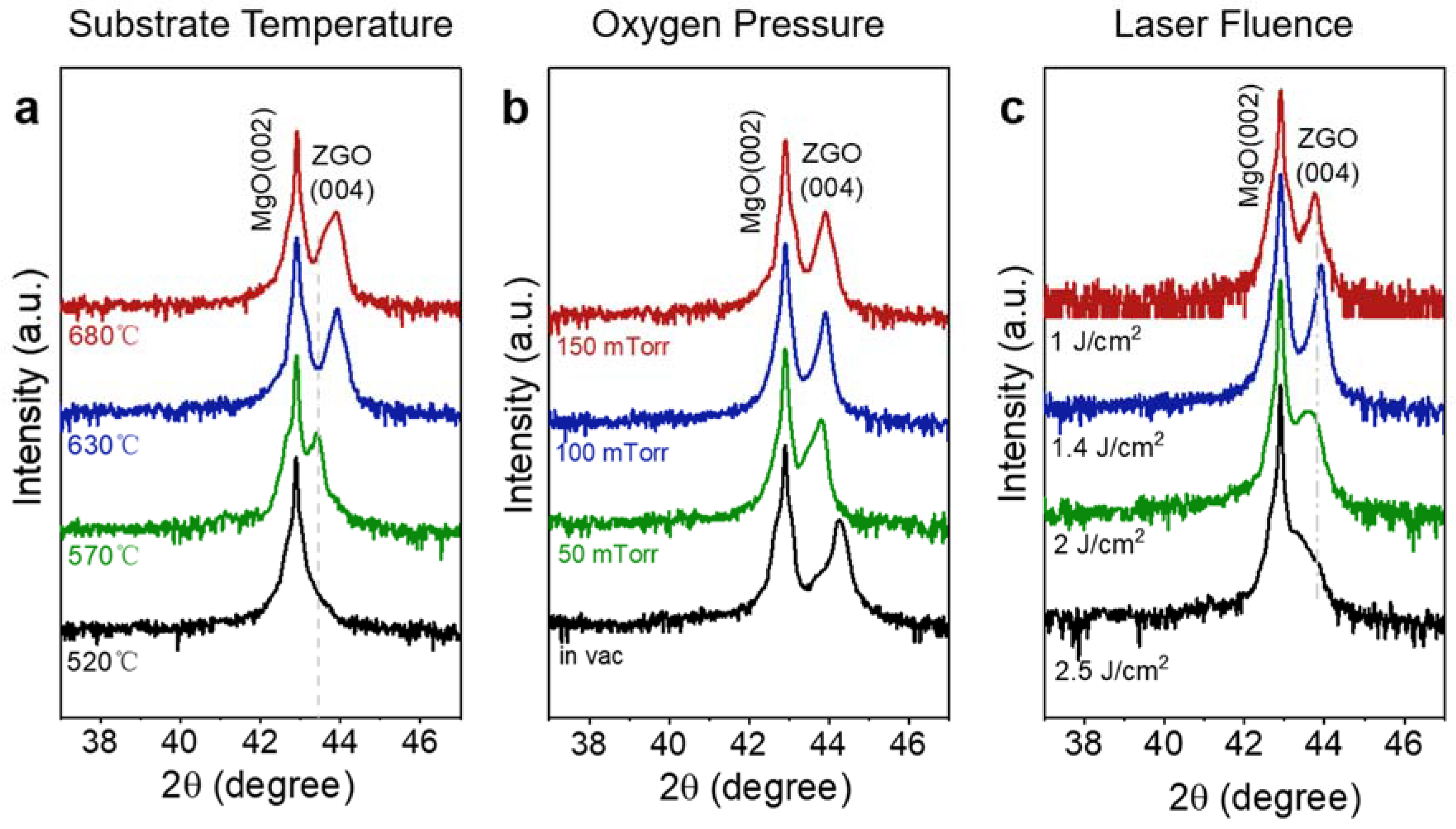
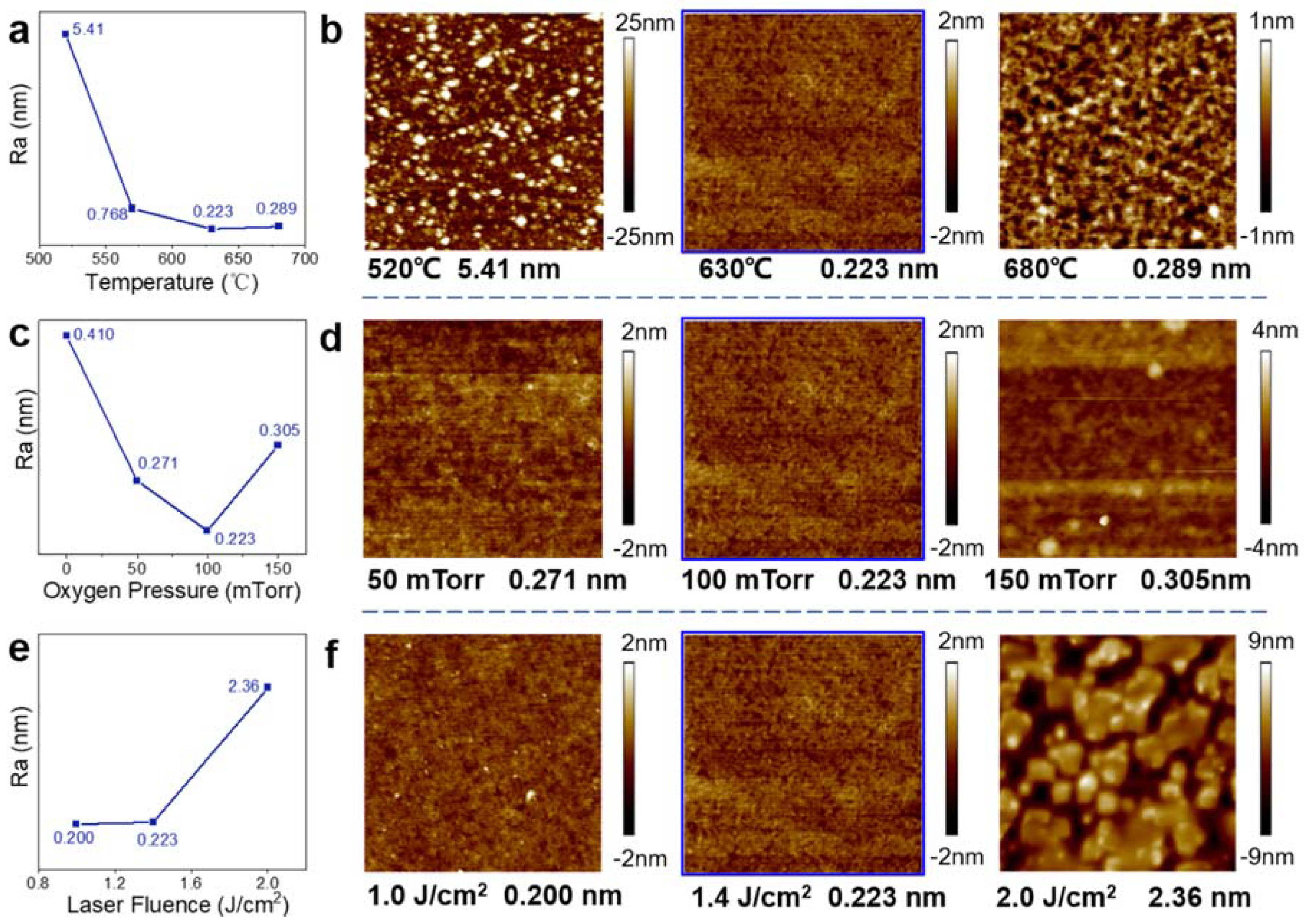
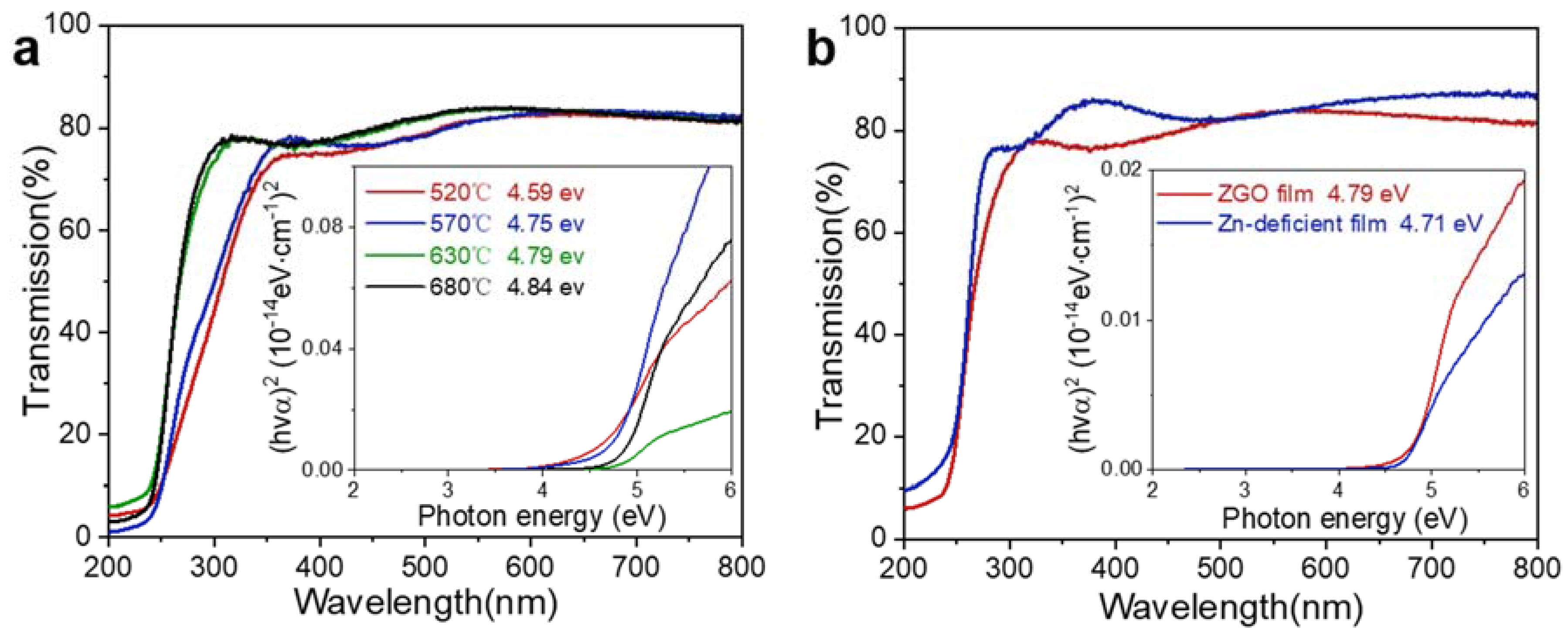
2. Result and Discussion

The stoichiometry difference of Zn1+xGa2O4 targets is readily seen from their distinct plume color during the laser ablation process (Figure 2a), which further impacts the film phase and chemical composition. According to the X-ray diffraction (XRD) scans, the film deposited by the non-stoichiometric Zn1+xGa2O4 (x = 6.5) target is a single-crystalline, phase-pure ZGO films with (00l) as its out-of-plane direction (Figure 2b). The energy-dispersive X-ray spectroscopy (EDX) analysis reveals a Zn:Ga molar ratio close to 1:2 for the same single-crystalline ZGO film (Figure 2c). On the other hand, the film deposited by the stochiometric Zn1+xGa2O4 target (x = 0) presents impurity Ga2O3 phase with mixed orientations, which suggests significant Zn loss during the PLD growth. This is further verified by the EDX analysis, since nearly no ZnO signal is observed from the Zn-deficient film (Figure 2c). High-resolution X-ray photoelectron spectroscopy (XPS) determines the primary oxidation states of Ga and Zn to be 3+ and 2+, respectively (Figure 2d,e). The Zn 2p peak for the Zn-deficient films is much weaker than that of the phase-pure ZGO film, which is consistent with the EDX result. The XPS spectra for the O 1s core level identify a stronger peak shoulder at 532.5 eV for the ZGO film (Figure 2f), which suggests different oxygen defect profile between these two films. Careful control of oxygen defect formation and distribution is recognized to be critical to fabricate high-performance photodetector, as they can readily impact carrier transport and recombination process [30,31,32].
We systematically investigate the film growth behavior as a function of different growth parameters, including growth temperature, oxygen pressure and laser fluence. We first discuss the epitaxial growth behavior based on the XRD results. The XRD pattern mainly appears near the MgO (002) peak, and no other peaks are observed in the full-scan results (Supplementary Material Figure S1). It is found that the film crystallinity starts to appear as the growth temperature reaches 570 °C (Figure 3a). As the substrate temperature further increases, the ZGO (004) peak shifts towards the higher angle direction, which reflects that the out-of-plane lattice parameter reduces from 43.42 Å at 570 °C and 43.87 Å at 680 °C. The film crystallinity is evaluated using the FWHM (full width at half maximum) value of the ZGO (004) peak. At ~630 °C, the ZGO film exhibits the smallest FWHM value of 0.6 degree, suggesting the highest crystallinity. The effect of oxygen pressure on the ZGO film growth is relatively minor as the growth pressure ranges from 150 mTorr to 50 mTorr (Figure 3b). Further reducing the oxygen pressure to vacuum (~1 × 10⁻⁶ Pa) leads to a broader film peak and the lattice compression along the out-of-plane direction. This can be understood by that a certain amount of oxygen is required during the ZGO film growth to suppress the formation of oxygen vacancy and reduce the lattice distortion. The laser fluence optimization is further performed, which identifies an optimized value of 1.4 J/cm2 that contributes to the highest film crystallinity (Figure 3c).
The influence of the above growth parameters on surface morphology is examined by atomic force microscopy, which is closely related to the film crystallinity evolution. The AFM image highlighted by the blue line in Figure 4 corresponds to the optimized film that are deposited under the growth condition of 630 °C, 100 mTorr,1 J/cm2. Increasing the growth temperature above 520 °C dramatically reduces the film surface roughness. At 630 °C, the ZGO film exhibits an extremely smooth morphology with a room-mean-square surface roughness (Ra) as low as 0.223 nm (Figure 4a,b). The zero-height value in the AFM images is an average between the deepest point and the highest point on the film surface. The ZGO films grown in the range of oxygen pressure between 50 mTorr to 150 mTorr presents similar morphology that is featured by a homogenous and smooth surface (Figure 4c,d). This is in sharp contrast to the film grown in vacuum, which shows particulate formation and Ga2O3 segregation (Figure S2). EDX analysis of the region containing particulates identifies a Zn/Ga ratio far less than 0.5, which suggests that the segregated particles in the AFM image are likely related to Ga2O3 precipitated phase. Using the optimized laser fluence of 1.4 J/cm2, the ZGO film presents the smallest surface roughness second only to 1 J/cm2 (Figure 4e,f).
The film growth evolution and stoichiometry modification have clear impact on the physical properties. The optical absorption spectrum is measured using UV-Vis spectroscopy, and the band gap is analyzed with the Tauc plot method [33]. It is found that higher growth temperature apparently enhances the band gap of as-synthesized ZGO films. Compared to the sharp absorption edge at 310 nm for films grown at 630 °C and 680 °C, the films grown at lower temperature presents noticeable absorption from 360–800 nm (Figure 5a). Such phenomenon likely arises from more defect formation in films with lower crystallinity, which contributes to the red-shift of the absorption edge [25]. Based on the Tauc plot method, it is found these epitaxial ZGO films have a direct gap around 4.8 eV, which is consistent with its bulk values [34]. Similar impact of the laser fluence on the optical absorption is observed (Figure S3a), while the oxygen pressure shows much less impact (Figure S3b).
We further compare the optical absorption properties of stochiometric ZGO film and Zn-deficient film. The thickness of these two films is ~120 nm. It is found that these two films have very similar optical gap values, with 4.79 eV for the stochiometric ZGO film and 4.71 eV for Zn-deficient film (Figure 5b). This is expected as the Ga2O3 phase in the Zn-deficient film has similar band gap (4.7–4.9 eV) [9,18] to the stoichiometric ZGO film (4.6–5.2 eV) [35,36]. On the other hand, the formation of Ga2O3 in the Zn-deficient film apparently reduces the thermal conductivity compared to the stoichiometric ZGO film. At 300 K, the thermal conductivity of the ZGO film grown on the MgO substrate is 40.137 W/(m⋅K), representing 22.10% larger than that of the Zn-deficient film (Figure 6). Such trend is consistent as the measurement temperature increases from 300 K to 700 K, suggesting that the low conductivity feature in Ga2O3 dominates the overall behavior of the Zn-deficient film. Although the measured thermal conductivity reflects the overall performance of both the film and the substrate, the reduced value for the stochiometric ZGO film reveals the significant role of stoichiometry control and phase stabilization on tuning the resulting physical properties.

3. Conclusions

We report the growth of epitaxial ZnGa2O4 films by pulsed laser deposition with a non-stoichiometric Zn1+xGa2O4 (x = 6.5) target. The optimized growth condition was determined to be 630 °C of substrate temperature, 100 mTorr of oxygen pressure, and 1.4 J/cm2 of laser fluence. Introducing a Zn-rich target effectively compensates the Zn volatilization and overcomes the problem of impurity Ga2O3 phase formation during the film growth. We systematically investigate the influence of various growth parameters on the phase formation, crystallinity and surface morphology of ZGO films, which further affects their optical property and thermal conductivity. A 120-nm-thick epitaxial ZGO film exhibits high crystallinity with a full width at half maximum value of 0.6 degree, smooth surface with a roughness of 0.223 nm, a direct optical gap of 4.79 eV and a room-temperature thermal conductivity of 40.137 W/(m⋅K). This study reveals the critical role of stoichiometry control in synthesizing epitaxial ZnGa2O4 films for advanced device application.

4. Experimental Section

4.1. Thin Film Deposition

ZnGa2O4 thin films were grown on single-crystalline MgO (100) substrates by pulsed laser deposition using a KrF excimer laser (λ = 248 nm). The target-substrate distance was 50 mm and the repetition rate was 5 Hz. The thin film growth optimization was performed by adjusting oxygen pressure (0–150 mTorr), substrate temperature (520–680 °C) and laser fluence (1.4–2.5 J/cm2). The film thickness varies from 90 to 230 nm by controlling the laser shot number. The laser-ablated ZnxGa2-xO4 targets with different x ratios are prepared using a conventional ceramic sintering method. In brief, high-purity Ga2O3 [Aladdin, 99.99%] and ZnO powders [Aladdin, 99.99%] are weighed in designed ratios, and subsequently mixed and sintered in air at 1200 °C for 6 h. The sintered powders are then pressed into disks and sintered in air at 1300 °C for 6 h.

4.2. Structural and Chemical Characterization

The ZnGa2O4 film phase composition, crystallinity and element content have investigated using X-ray diffraction (XRD, Bruker D8 ADVANCE, Billerica, MA, USA) and scanning electron microscopy (SEM, HITACHI Regulus-8230, Tokyo, Japan). Atomic force microscopy (AFM, Bruker Dimension Icon, Billerica, MA, USA) is used to measure the surface morphology. X-ray photoemission spectroscopy (XPS, Kratos AXIS SUPRA, Tokyo, Japan) measurements were performed in an ultrahigh vacuum system using Mg Kα (hν = 1253.6 eV) as the excitation source. The transmission spectrum was measured by ultraviolet-visible spectroscopy (UV-Vis, Perkin Elmer Lambda 950, Waltham, MA, USA) in the range of 300–700 K. Thermal analyzer (TA, NETZSCH LFA 457 MicroFlash, Selb, Germany) is used to probe the ability to conduct heat of the ZGO film over the MgO substrates, so the measured thermal conductivity is an average of film and substrate. Since both films are grown on the same type of MgO, so we can compare their thermal conductivity.

Supplementary Materials

The Supporting Information is available on https://www.mdpi.com/article/10.3390/coatings11070782/s1. X-ray diffraction (XRD) results of ZnGa2O4 films, Atomic force microscopes (AFM) of film deposited in vacuum, Energy-dispersive X-ray spectra (EDX) of the thin film deposited in vacuum, the transmission spectrum and the calculated bandgap width diagram of the thin films.

Author Contributions

W.Z., Z.Z. and J.Y. conceived the project and designed the project. L.W., N.L., T.Z. fabricated the samples and performed the UV-Vis, EDX, XPS, thermal property measurements. Z.W. and S.W. performed part of XRD and AFM measurements. L.W. and W.Z. analyzed the results and wrote the manuscript. All authors discussed the results and commented on the manuscript. All authors have read and agreed to the published version of the manuscript.

Funding

This research was funded by the National Natural Science Foundation of China, grant number 62004200 and by Zhejiang Provincial Natural Science Foundation of China LZ21F040001. N.L. acknowledges the support from the Outstanding Research Associate Funding of Chinese Academy of Sciences.

Conflicts of Interest

The authors declare no conflict of interest.

References

  1. Kan, H.; Zheng, W.; Lin, R.; Li, M.; Fu, C.; Sun, H.; Dong, M.; Xu, C.; Luo, J.; Fu, Y.; et al. Ultrafast photovoltaic-type deep ultraviolet photodetectors using hybrid zero-/two-dimensional heterojunctions. ACS Appl. Mater. Interfaces 2019, 11, 8412–8418. [Google Scholar] [CrossRef] [Green Version]
  2. Xie, C.; Lu, X.-T.; Tong, X.-W.; Zhang, Z.-X.; Liang, F.-X.; Liang, L.; Luo, L.-B.; Wu, Y.-C. Recent progress in solar-blind deep-ultraviolet photodetectors based on inorganic ultrawide bandgap semiconductors. Adv. Funct. Mater. 2019, 29, 1806006. [Google Scholar] [CrossRef]
  3. Chen, H.; Liu, K.; Hu, L.; Al-Ghamdi, A.A.; Fang, X. New concept ultraviolet photodetectors. Mater. Today 2015, 18, 493–502. [Google Scholar] [CrossRef]
  4. Fan, M.M.; Liu, K.W.; Chen, X.; Wang, X.; Zhang, Z.Z.; Li, B.H.; Shen, D.Z. Mechanism of excellent photoelectric characteristics in mixed-phase ZnMgO ultraviolet photodetectors with single cutoff wavelength. ACS Appl. Mater. Interfaces 2015, 7, 20600–20606. [Google Scholar] [CrossRef] [PubMed]
  5. Zhou, X.; Zhang, Q.; Gan, L.; Li, X.; Li, H.; Zhang, Y.; Golberg, D.; Zhai, T. High-performance solar-blind deep ultraviolet photodetector based on individual single-crystalline Zn2GeO4 nanowire. Adv. Funct. Mater. 2016, 26, 704–712. [Google Scholar] [CrossRef]
  6. Liao, M.; Koide, Y. High-performance metal-semiconductor-metal deep-ultraviolet photodetectors based on homoepitaxial diamond thin film. Appl. Phys. Lett. 2006, 89, 113509. [Google Scholar] [CrossRef]
  7. Kaur, D.; Kumar, M. A strategic review on gallium oxide based deep—Ultraviolet photodetectors: Recent progress and future prospects. Adv. Opt. Mater. 2021, 9, 2002160. [Google Scholar] [CrossRef]
  8. Qin, Y.; Li, L.; Zhao, X.; Tompa, G.S.; Dong, H.; Jian, G.; He, Q.; Tan, P.; Hou, X.; Zhang, Z.; et al. Metal-semiconductor-metal ε-Ga2O3 solar-blind photodetectors with a record-high responsivity rejection ratio and their gain mechanism. ACS Photonics 2020, 7, 812–820. [Google Scholar] [CrossRef]
  9. Galazka, Z.; Ganschow, S.; Schewski, R.; Irmscher, K.; Klimm, D.; Kwasniewski, A.; Pietsch, M.; Fiedler, A.; Schulze-Jonack, I.; Albrecht, M.; et al. Ultra-wide bandgap, conductive, high mobility, and high quality melt-grown bulk ZnGa2O4 single crystals. APL Mater. 2019, 7, 022512. [Google Scholar] [CrossRef] [Green Version]
  10. Chen, P.W.; Huang, S.Y.; Yuan, S.H.; Chen, Y.A.; Hsiao, P.W.; Wuu, D.S. Quasi-single-crystalline ZnGa2O4 films via solid phase epitaxy for enhancing deep—ultraviolet photoresponse. Adv. Mater. Interfaces 2019, 6, 1901075. [Google Scholar] [CrossRef]
  11. Noto, L.L.; Mbongo, M. Photoluminescence and thermoluminescence properties of ZnGa2O4 prepared by a microwave assisted solid state reaction. Phys. B Condens. Matter 2020, 578, 411768. [Google Scholar] [CrossRef]
  12. Horng, R.-H.; Huang, C.-Y.; Ou, S.-L.; Juang, T.-K.; Liu, P.-L. Epitaxial growth of ZnGa2O4: A new, deep ultraviolet semiconductor candidate. Cryst. Growth Des. 2017, 17, 6071–6078. [Google Scholar] [CrossRef]
  13. Oshima, T.; Niwa, M.; Mukai, A.; Nagami, T.; Suyama, T.; Ohtomo, A. Epitaxial growth of wide-band-gap ZnGa2O4 films by mist chemical vapor deposition. J. Cryst. Growth 2014, 386, 190–193. [Google Scholar] [CrossRef]
  14. Chen, H.; Yu, P.; Zhang, Z.; Teng, F.; Zheng, L.; Hu, K.; Fang, X. Ultrasensitive self-powered solar-blind deep-ultraviolet photodetector based on all-solid-state polyaniline/MgZnO bilayer. Small 2016, 12, 5809–5816. [Google Scholar] [CrossRef]
  15. Hou, Y.N.; Mei, Z.X.; Liang, H.L.; Ye, D.Q.; Gu, C.Z.; Du, X.L. Dual-band MgZnO ultraviolet photodetector integrated with Si. Appl. Phys. Lett. 2013, 102, 153510. [Google Scholar] [CrossRef] [Green Version]
  16. Yoshida, S.; Misawa, S.; Gonda, S. Properties of AlxGa1−xN films prepared by reactive molecular beam epitaxy. J. Appl. Phys. 1982, 53, 6844–6848. [Google Scholar] [CrossRef]
  17. Cicek, E.; McClintock, R.; Cho, C.Y.; Rahnema, B.; Razeghi, M. AlxGa1-xN-based back-illuminated solar-blind photodetectors with external quantum efficiency of 89%. Appl. Phys. Lett. 2013, 103, 191108. [Google Scholar] [CrossRef]
  18. Xu, J.; Zheng, W.; Huang, F. Gallium oxide solar-blind ultraviolet photodetectors: A review. J. Mater. Chem. C 2019, 7, 8753–8770. [Google Scholar] [CrossRef]
  19. Cheng, L.-C.; Huang, C.-Y.; Horng, R.-H. Thickness effect on operational modes of ZnGa2O4 MOSFETs. J. Electron Devices Soc. 2018, 6, 432–437. [Google Scholar] [CrossRef]
  20. Zhang, W.; Zhang, J.; Li, Y.; Chen, Z.; Wang, T. Preparation and optical properties of ZnGa2O4:Cr3+ thin films derived by sol–gel process. Appl. Surf. Sci. 2010, 256, 4702–4707. [Google Scholar] [CrossRef]
  21. Choi, H.-W.; Hong, B.-J.; Lee, S.-K.; Kim, K.-H.; Park, Y.-S. Cathode luminescence characteristics of ZnGa2O4 phosphor thin films with the doped activator. J. Lumin. 2007, 126, 359–364. [Google Scholar] [CrossRef]
  22. Yi, S.S.; Bae, J.S.; Shim, K.S.; Jeong, J.H.; Park, H.L.; Holloway, P.H. Photoluminescence behavior of ZnGa2O4−xSex: Mn2+ thin film phosphors. J. Cryst. Growth 2003, 259, 95–102. [Google Scholar] [CrossRef]
  23. Dazai, T.; Yasui, S.; Taniyama, T.; Itoh, M. Cation-deficiency-induced crystal-site engineering for ZnGa2O4: Mn(2+) thin film. Inorg. Chem. 2020, 59, 8744–8748. [Google Scholar] [CrossRef]
  24. Mini Krishna, K.; Nisha, M.; Reshmi, R.; Manoj, R.; Asha, A.S.; Jayaraj, M.K. Electrical and optical properties of ZnGa2O4 thin films deposited by pulsed laser deposition. Mater. Sci. Forum 2005, 29, 243–247. [Google Scholar]
  25. Zhang, W.; Lyons, J.L.; Cen, J.; Sfeir, M.Y.; Liu, M. Multicomponent oxynitride thin films: Precise growth control and excited state dynamics. Chem. Mater. 2019, 31, 3461–3467. [Google Scholar] [CrossRef]
  26. Yia, S.S.; Kim, I.W.; Park, H.L.; Bae, J.S.; Moon, B.K.; Jeong, J.H. Luminescence characteristics of pulsed laser deposited ZnGa2O4 thin film phosphors grown on various substrates. J. Cryst. Growth 2003, 247, 213–218. [Google Scholar] [CrossRef]
  27. Lee, Y.E.; Norton, D.P.; Park, C.; Rouleau, C.M. Blue photoluminescence in ZnGa2O4 thin-film phosphors. J. Appl. Phys. 2001, 89, 1653. [Google Scholar] [CrossRef]
  28. Lee, Y.E.; Norton, D.P.; Budai, J.D. Enhanced photoluminescence in epitaxial ZnGa2O4:Mn thin-film phosphors using pulsed-laser deposition. Appl. Phys. Lett. 1999, 74, 3155–3157. [Google Scholar] [CrossRef]
  29. Jang, Y.; Hong, S.; Seo, J.; Cho, H.; Char, K.; Galazka, Z. Thin film transistors based on ultra-wide bandgap spinel ZnGa2O4. Appl. Phys. Lett. 2020, 116, 202104. [Google Scholar] [CrossRef]
  30. Zhang, W.; Song, L.; Cen, J.; Liu, M. Mechanistic insights into defect-assisted carrier transport in bismuth vanadate photoanodes. J. Phys. Chem. C 2019, 123, 20730–20736. [Google Scholar] [CrossRef]
  31. Tsai, S.H.; Basu, S.; Huang, C.Y.; Hsu, L.C.; Lin, Y.G.; Horng, R.H. Deep-ultraviolet photodetectors based on epitaxial ZnGa2O4 thin films. Sci. Rep. 2018, 8, 14056. [Google Scholar] [CrossRef] [PubMed]
  32. Shen, Y.-C.; Huang, P.-H.; Tung, C.-Y.; Huang, C.-Y.; Tan, C.-S.; Huang, Y.-S.; Chen, L.-J.; He, J.-H.; Horng, R.-H. Power saving high performance deep-ultraviolet phototransistors made of ZnGa2O4 Epilayers. ACS Appl. Electron. Mater. 2020, 2, 590–596. [Google Scholar] [CrossRef]
  33. Kim, H.; Horwitz, J.S.; Kim, W.H.; Kafafi, Z.H.; Chrisey, D.B. Highly oriented indium tin oxide films for high efficiency organic light-emitting diodes. J. Appl. Phys. 2002, 91, 5371–5376. [Google Scholar] [CrossRef]
  34. Shi, Q.; Wang, C.; Zhang, D.; Li, S.; Zhang, L.; Wang, W.; Zhang, J. Luminescence of Cr3+-doped ZnGa2O4 thin films deposited by pulsed laser ablation. Thin Solid Films 2012, 520, 6845–6849. [Google Scholar] [CrossRef]
  35. Yamaguchi, K. First principles study on electronic structure of β-Ga2O3. Solid State Commun. 2004, 131, 739–744. [Google Scholar] [CrossRef]
  36. Chikoidze, E.; Sartel, C.; Madaci, I.; Mohamed, H.; Vilar, C.; Ballesteros, B.; Belarre, F.; del Corro, E.; Vales-Castro, P.; Sauthier, G.; et al. P-type ultrawide-band-gap spinel ZnGa2O4: New perspectives for energy electronics. Cryst. Growth Des. 2020, 20, 2535–2546. [Google Scholar] [CrossRef]
Figure 1. (a) The schematic diagram of the ZnGa2O4 film growth by PLD. The severe volatilization of Zn occurs during the ZnGa2O4 film growth due to the much higher vapor pressure of Zn than that of Ga. (b) The film deposited by a stochiometric target exhibits phase segregation due to Zn volatilization, which leads to the formation of impurity Ga2O3 phase. But the film deposited by a Zn-rich target is single-crystalline due to supplementing excessive Zn during the thin film growth.
Coatings 11 00782 g001
Figure 2. (a) The laser-ablation plume image deposited by ZGO targets with different Zn/Ga ratios. (b) θ-2θ XRD scans of phase-pure ZGO film and Zn-deficient film on MgO deposited by different Zn/Ga ratio targets showing c-axis-oriented growth. (c) EDX spectra of phase-pure ZGO film and Zn-deficient film. Inset is the enlarged image with film EDX spectra of 8–11 keV. High-resolution XPS spectra of (d) Ga 2p, (e) Zn 2p, and (f) O 1s core levels in phase-pure ZGO film and the Zn-deficient film.
Coatings 11 00782 g002
Figure 3. θ-2θ XRD scans of ZGO films over MgO showing c-axis-oriented growth which are deposited under different conditions of (a) substrate temperature, (b) oxygen pressure and (c) laser fluence.
Coatings 11 00782 g003
Figure 4. Room-mean-square surface roughness (Ra) and topology AFM image (scan area of 2 × 2 μm2) of the ZGO films deposited under different growth conditions.
Coatings 11 00782 g004
Figure 5. Thin film transmission as a function of excitation wavelength for ZGO films with (a) different substrate temperatures and (b) targets with different Zn/Ga ratios. Inset shows a linear extrapolation of Eg for ZGO films from their UV−Visible transmission spectra.
Coatings 11 00782 g005
Figure 6. Thermal conductivity of a stochiometric ZGO film deposited from a Zn-rich ZGO target and a Zn-deficient film deposited from a ZGO target.
Coatings 11 00782 g006
Publisher’s Note: MDPI stays neutral with regard to jurisdictional claims in published maps and institutional affiliations.

