Abstract
The current work examines the effects of cesium lead bromide (CsPbBr3) perovskite quantum dots (PQDs) on the structural and optical properties of conjugated polymer blends of poly[2-methoxy-5-(2′-ethylhexyloxy)-1,4-phenylene vinylene] (MEH–PPV) and poly(9,9-di-n-octylfluorenyl-2,7-diyl) (PFO). MEH–PPV/PFO composite thin-films containing PQDs with weight ratios between 0.5 wt.% and 10 wt.% were prepared via a solution-blending method prior to spin-coating on glass substrates. The MEH–PPV/PFO composites’ crystallinity was improved, and the roughness was dramatically increased with higher PQDs content, as confirmed by X-ray diffraction (XRD) and atomic force microscopy (AFM), respectively. Conversely, a higher PQDs content resulted in a gradual reduction of the Urbach tail and an increase in the steepness parameter, thereby reducing the localized density of the electronic states within the forbidden bandgap of the hybrids. Moreover, a slight reduction in the direct and indirect bandgaps was found in PQDs/(MEH–PPV/PFO) composite films containing a higher PQDs content and provided evidence of the low concentration of the localized states. The incorporation of the PQDs resulted in enhanced non-radiative energy transfer processes in the MEH–PPV/PFO hybrids, which are very important for the development of optimized optoelectronic devices.
1. Introduction
Over the past two decades, researchers have focused most of their efforts on the development and characterization of perovskite materials. Recently, extensive work has been done on perovskite−polymer composites, in particular, on organic–inorganic lead halide perovskite composites that are capable of increasing the power conversion efficiency of photovoltaic devices and appeared efficient in light-emitting applications. The optical characteristics of these perovskite−polymer composite materials can be easily adjusted via simple substitution of their components, which enables researchers to “mix and match” the physical, chemical, and electrical properties of the product. A classic example of this can be seen in organic–inorganic lead iodide perovskites; these composites exhibit strong bandgap absorption at around 1.6 eV, making this class of materials one of the most widely used compounds in photovoltaic applications. On the other hand, substitution of the iodide with bromide results in a bandgap of around 2.3 eV, which is ideally suited for visible laser and light-emitting applications. In both cases, the material’s activity is due to its high photoluminescence quantum yield (PLQY), which facilitates the efficient conversion of the optically or electrically generated charges into photons [1,2,3,4,5]. There have been many attempts to narrow the sizeable optical bandgap and fine-tune the energy levels of CsPbBr3 perovskite quantum dots (PQDs) and poly[2-methoxy-5-(2′-ethylhexyloxy)-1,4-phenylene vinylene] (MEH–PPV)/poly(9,9-di-n-octylfluorenyl-2,7-diyl) (PFO)-conjugated polymers to enhance the laser and light-emitting applications [6,7]. Accurately defining the bandgap in materials is very important, as it is an indication of the energy difference between the top of the electron-rich valence band (VB) and the bottom of the electron-deficient conduction band (CB) [8]. Since perovskites can absorb only photons in the UV–Vis region due to their wide bandgaps, conjugation with a polymer narrows the bandgap and facilitates the absorption of photons in the NIR region. Furthermore, these polymer-conjugated compounds are soluble, have tunable energy levels, and exhibit efficient charge separation at p–n junctions [9]. As a result, they are popular light absorbers in tandem polymer solar cells [10] and are crucial components of integrated perovskite–polymer bulk heterojunction solar cells [11,12]. A hybrid method was utilized to prepare CH3NH3PbBr3 perovskite–alumina nanoparticle composites with a high PLQY value of up to 39% [1]. Photoluminescence in these compounds was significantly improved as a result of the formation of perovskite nanocrystals. Moreover, these materials were very stable during solution-to-air transitions at low temperatures and were unsusceptible to moisture, making them promising candidates for future light-emitting and laser applications [1].
Luminescent perovskite nanocrystals could be embedded in a pinhole-free matrix of the dielectric polymer without the need for precise control protocols or modification of the crystallite surfaces for light-emitting diodes. These findings highlighted the benefits of film formation in solution-processed perovskite solar cells in alleviating shunt resistance problems [2]. A white perovskite light-emitting diode (PeLED) was first produced by blending orange polymer materials with blue perovskite nanocrystals, which served as the active layer [3]. The transfer of excitons from the blue nanocrystals to the orange polymer via Förster or Dexter energy transfer processes was observed via time-resolved photoluminescence spectroscopy, and white-light emissions were achieved by tuning the ratio between the nanocrystals and the polymers [3]. The green emissive MAPbBr3–polymer composite films and red CdSe-based quantum dots (QD) polymer films, which served as down converters for blue light-emitting devices (LEDs), exhibited white-light luminescence with a record 95% color gamut in Rec. 2020, thereby becoming the new color standard for ultra-high-definition TVs [5]. A unique approach for the one-pot preparation of the perovskite–polymer matrix was reported; here, no organic solvent was needed, thereby significantly simplifying the synthetic route by eliminating many tedious separation and preparation procedures. The quantum yield of these composites remained stable after continuous exposure to air for more than a month. Based on the characteristics mentioned above, white light-emitting diode prototypes with narrow bandwidths and feasible color characteristics were successfully prepared. Researchers have been striving to improve the efficiency of these composites; one notable example of this was reported in 2016, in which the power conversion efficiency of a solar cell composed of poly(methyl methacrylate) (PMMA) and perovskite composites was as high as 22.1% [13]. Although many published reports agree that the chemical stability inferred by conjugating polymers with perovskite crystals could be beneficial for numerous advanced applications, the properties of these composites as they relate to optical purposes demand more detailed analysis and investigation [14,15,16,17]. In our previous work [18], we noted that blending PFO with CsPbBr3-QDs improved the thin-film’s morphology, tuned the optical properties of the thin-film, and facilitated non-radiative energy transfer (i.e., Förster-type transfers) from PFO to CsPbBr3-QDs. Förster energy transfers are important factors as they are responsible for enhancing electron–hole recombination processes.
Herein, high-quality green-emitting CsPbBr3-QDs (PQDs in this work), which act as acceptors, were incorporated into blends of poly [2-methoxy-5-(2-ethyl-hexyloxy)-1,4-phenylene-vinylene] (MEH–PPV) and poly[9,9-di-n-octylfluorenyl-2,7-diyl] (PFO) by using the solution blending method to create a new class of nanocomposites on smooth, high-quality thin-films in one straightforward step. In our previous works, the effect of the variation of the MEH/PPV on the improvement of photophysical properties of the PFO was demonstrated [19,20]. The main purpose of this work was to determine the effects of various PQDs concentrations in hybrid MEH–PPV/PFO conjugated polymer composites on the structural and optical properties using several characterization techniques, including transmission electron microscopy (TEM), atomic force microscopy (AFM), X-ray diffraction (XRD), UV–Vis, and photoluminescence (PL) spectroscopy. Here, characteristics such as crystallization, roughness, bandgap energy, the localized states, and the Urbach energy (which describes the shrinkage/broadening of the optical absorption edge via the steepness parameter) were investigated. Additionally, evidence of enhanced non-radiative energy transfers in the hybrid thin films was obtained by varying the PQD content of the composites. With this study, we showed how incorporating various ratios of PQDs could “tune” the optical properties and electronic structure of these hybrid polymer composites.
2. Experimental
2.1. Materials
MEH–PPV (Mw = 51,000 g/mol), PFO (Mw = 58,200 g/mol), and toluene (anhydrous, >99.9%) were purchased from Sigma–Aldrich (Saint Louis, MO, USA) and used as received without further purification. High-quality green-emitting CsPbBr3-QDs (PQDs) were purchased from Quantum Solutions Company (Thuwal, Saudi Arabia, www.qdot.inc). All materials were used as soon as they were received.
2.2. Methods
Stock solutions were prepared in an anhydrous organic solvent such as toluene. The preparation of the perovskite–polymer blend was organized to facilitate the protection of the PQDs and avoid redundant steps. Although various methods have been used to synthesize the perovskite–polymer blends, issues related to heterogeneous phase aggregation and the moisture-dependent decomposition of the perovskites occurred. The perovskites were prepared before blending, and both the preparation and storage of the prepared perovskites required careful handling under protective conditions to improve the properties of the perovskite−polymer composite products. The conjugated polymers (MEH–PPV/PFO) hybrid was prepared as stock solutions in toluene (PFO in 0.5 wt.% MEH–PPV). Briefly, the PQDs powder was dissolved in a certain amount of toluene to get the required concentration of 20 mg/mL and left overnight to facilitate better dispersion and complete dissolution. The MEH–PPV/PFO blend was prepared using 0.5 wt.% MEH–PPV under ultrasonication for 1 h to obtain a homogeneous solution.
Prior to spin-coating, the glass substrates were sonicated sequentially in soapy water and water for 15 min each. Then, acetone and isopropyl alcohol were added separately and sonicated for 15 min each. The solutions of MEH–PPV/PFO and PQDs were premixed via the solution blending method to generate transparent precursor solutions containing various weight ratios of PQDs, namely, 0.5 wt.%, 1 wt.%, 3 wt.%, 5 wt.%, 7 wt.%, and 10 wt.%. Then, 50 µL of each sample was added to the cleaned glass substrates dropwise. Spin-coating at 2500 rpm for 30 s produced homogenous thin-films that were annealed at 120 °C in a vacuum oven to remove any remaining solvent [21].
2.3. Characterizations
A (JEOL JEM-2100F) high-resolution transmission electron microscope (HRTEM) (JEOL, Tokyo, Japan) was employed to determine the structures and sizes of the respective CsPbBr3-QDs. The samples structures were characterized using a Rigaku Miniflex 600 XRD system (Rigaku, Tokyo, Japan) under Cu Kα radiation (λ = 1.5418 Å). The scanning angle (2θ) varied between 10° and 80° at increments of 0.02° and a scan speed of 3° min−1. Additionally, Atomic Force Microscope (AFM) Characteristics using Multimode V Scan Probe Microscope (Nanoscope V, Veeco, Santa Barbara, CA, USA) was conducted using a Veeco multimode V SPM to characterize the films’ morphology.
The optical properties of the thin films were determined by obtaining absorption and photoluminescence spectra using a UV-VIS-NIR spectrophotometers JASCO V-630 (JASCO, Cremella, Italy) an absorption spectrometer, and a JASCO FP-8200 spectrofluorometer (JASCO, Cremella, Italy), respectively. The excitation wavelength for all samples was fixed at 350 nm. The thin film thickness was measured by a surface profilometer (Dektak 150, Bruker, Billerica, MA, USA). It was 200 and 300 nm for a hybrid of MEH–PPV/PFO and PQDs thin films, respectively, and it changed in the range of 205–240 nm upon increasing the PQDs in the hybrid thin films. All measurements were conducted under ambient conditions and atmosphere.
3. Results and Discussion
3.1. Structural Characteristics
A typical HRTEM image of the resulting PQDs is shown in Figure 1, indicating that CsPbBr3 QDs were successfully grown, and this is further confirmed by the measured XRD patterns shown in Figure 2. Here, the CsPbBr3 possessed QDs with diameters between 6 and 10 nm. For the TEM characterization, the CsPbBr3 QDs was prepared by the dilution of 10 μL from CsPbBr3 QDs solution with 2 mL of hexane followed by placing several drops of a dilute CsPbBr3 QDs solution onto a carbon-coated copper grid.
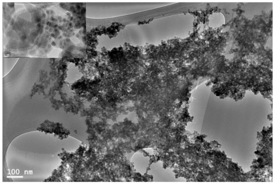
Figure 1.
TEM image of CsPbBr3 perovskite quantum dots (PQDs). The inset is TEM image with scale bar of 5 nm.
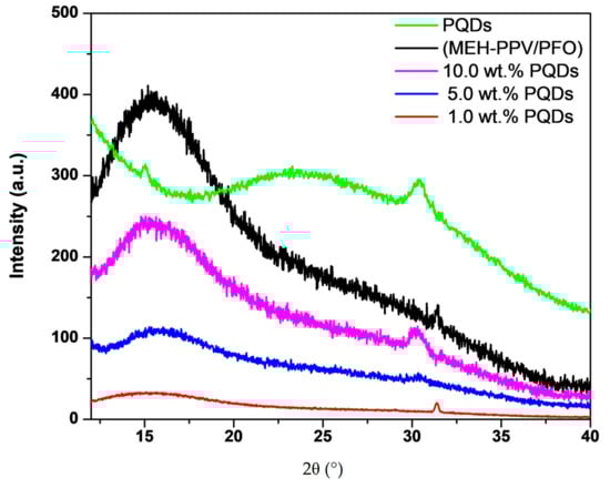
Figure 2.
XRD diffractograms of the poly[2-methoxy-5-(2′-ethylhexyloxy)-1,4-phenylene vinylene] (MEH–PPV)/poly(9,9-di-n-octylfluorenyl-2,7-diyl) (PFO) hybrid, CsPbBr3-PQDs, and PQDs/(MEH–PPV/PFO) composite thin-films.
The structure and orientation of the component crystals were determined via XRD, as shown in Figure 2. Scattering signals in the XRD patterns were obtained for the pure PQDs, the MEH–PPV/PFO-conjugated polymers, and the PQDs/(MEH–PPV/PFO) composite thin films. Unlike previously reported, the polymers did not readily absorb in the X-ray region [18,22], as evidenced by the XRD patterns of the experimental samples. Only one broad peak was observed for the MEH–PPV/PFO blend centered at 2θ of 15.55°. The broadened peak is indicative of the fully amorphous structure of the MEH–PPV/PFO blend [23,24,25]. In the XRD patterns, another broad peak centered at 2θ of 23.75° and two sharp peaks at 2θ of 15.03° and 30.42° were attributed to the (121), (101), and (202) planes of the perovskite crystals, respectively. These sharp peaks corresponded to the CsPbBr3-QDs and indicated that the film had adopted a polycrystalline cubic structure. The 2θ values of these peaks were in good agreement with previous reports [26,27]. Due to the small PQDs content in these hybrid thin films, only the main peak of the PQDs at 30.42° was observed in the XRD patterns of the PQDs/(MEH–PPV/PFO) thin films. The strong broad peak centered at 15.55° and the peak at 30.42° appeared in the X-ray patterns, confirming the formation of the respective PQDs/(MEH–PPV/PFO) composites in the current samples. Moreover, the crystallization improvement of the composites can be also proved from the decrease of the full width at half maximum (FWHM) of the peak at 30.42°.
The crystallite size (D), dislocation density (δ), and lattice strain (ε) are given by Equation (1):
where λ is the wavelength of the X-ray source, θ is the Bragg angle, and β is the full width at half maximum of the observed peak [28]. The addition of PQDs of various weight ratios significantly influenced the hybrid films’ structures and increased the grain size of the composite, which had been previously predicted using the increasing intensity of the (202) peak in the XRD diffraction studies. The XRD analysis results are summarized in Table 1, for 2θ = 30.42°, where the peak at 30.42° continues to appear after blending the PQDs with the MEH-PPV/PFO. The increase in the grain size could be attributed to the agglomeration of the PQDs on the MEH–PPV/PFO conjugated polymer segments. In addition, there are several effects that modify the growth of grains in a thin film, e.g., surface energy anisotropy. For grains with orientations that have very high surface energy, the grain boundaries will be driven to replace these grains with others of lower surface energy. In addition, the film and the substrate usually have no dislocations at the interface, leading to stresses in the film. This will lead to an increase in the grain growth rates in the film to reduce stresses [29]. Thus, changing the dislocation density and lattice strain values that occur upon the addition of the PQDs in the hybrid thin films may have led to imperfections, vacancies, and interstitials, resulting in a slight shift in the peak positions obtained from the XRD patterns.
D= 0.9 × λ/(βcosθ), δ = 1/D2, and ε= βcosθ/4

Table 1.
Structural properties of the MEH–PPV/PFO hybrid, CsPbBr3-PQDs, and PQDs/(MEH–PPV/PFO) composite thin films.
The AFM images of the above-mentioned MEH–PPV/PFO thin films are shown in Figure 3. According to these images, the surfaces of the PQDs/(MEH–PPV/PFO) composite thin films showed vast improvements when compared to the results obtained for the pristine CsPbBr3 thin film.
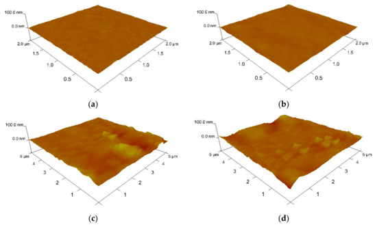
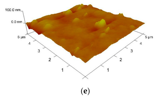
Figure 3.
Three-dimensional (3D) atomic force microscopy (AFM) images of (a) the MEH–PPV/PFO hybrid, (b) the CsPbBr3-PQDs, and (c–e) the PQDs/(MEH–PPV/PFO) composite films containing PQDs weight ratios of 1 wt.%, 5 wt.%, and 10 wt.%.
The root mean square (RMS) roughness of the CsPbBr3-PQDs thin film and MEH-PPV/PFO was 15.40 and 7.86 nm, respectively. It can be observed drastically increasing in the film roughness upon increasing the concentration of PQDs, as listed in Table 1. It was theorized that the smoother surface reduced the loss of the incident pumping light at the air/thin-film interface, which may be beneficial in lasing applications. Such an increase in the roughness may play a significant role in increasing a locally high electric field and thus improve the electron injection in the optoelectronic devices, resulting in reducing the turn-on voltage of the devices. It can optimize the device performance by tuning the thin film roughness, where the huge roughness leads to high aggregation and phase separation, causing high leakage current and a short-circuit device [30,31,32,33].
3.2. Optical Analysis
The absorption coefficient (α) was determined using the following relation:
where A and d are the values for absorbance and film thickness, respectively. This was done to highlight any changes to the structure of the electronic band of the composites and to determine the type of electron transition processes. Studying the optical absorption and the absorption edge of the composites provided useful information about the band structure and energy gap. The optical absorption coefficients spectra of the MEH–PPV/PFO thin films, which contained various concentrations of the PQDs, namely, 0.5, 1, 3 wt.%, 5 wt.%, 7 wt.%, and 10 wt.%, are shown in Figure 4.
α = 2.303 × (A/d)
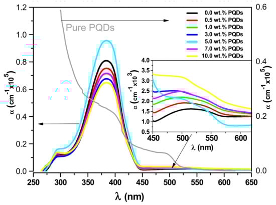
Figure 4.
The absorption coefficient Spectra of the MEH−PPV/PFO hybrid, the CsPbBr3−PQDs, and the PQDs/(MEH−PPV/PFO) composite thin-films as a function of the wavelength. The inset shows the magnification of the absorption coefficient spectra in the range of 450–625 nm.
Here, the maximum absorbance peak of the mixed MEH–PPV/PFO-conjugated polymers was observed at 384 nm (3.23 eV) with a shoulder at 292 nm (4.25 eV). The absorbance spectrum of the PQDs in Figure 4 contained broad bands with an absorption edge at 500 nm (2.48 eV). When the PQDs content in the hybrid thin films was increased, the peak at 500 nm (2.48 eV) was dramatically enhanced (shown in the inset in Figure 4). The peak at 510, which is related to the MEH-PPV [20], was gradually blue-shifted to 500 nm, and eventually, the shoulder peak of the PQDs became the dominant when the content of the PQDs increased to 10.0 wt.%. The PQDs/(MEH–PPV/PFO) composite films exhibited complementary absorption between 384 and 510 nm, making these hybrids useful for the fabrication of UV–Vis photodetectors.
The absorption coefficient, which was related to the incident photon energy, was used to identify the fundamental absorption edge when the electron is transferred from the lower to the higher energy states [34]. The lower photon energy region, referred to as the Urbach tail, is less than the bandgap energy and plays a role in generating defect states in the resulting thin film. Since defect states are essential for determining the electrical properties of thin-film semiconductors, their characterization allows researchers to assess the suitability of a thin film for a particular application or manufacture of a device [18,35]. These defect-induced local states can be characterized by investigating the spectral dependence of α in the lower photon energy region. Exponential Urbach tails can be observed as a result of electron–phonon interaction, impurities, excitons, and structural disorders in the materials. The Urbach energy can be determined from the inversed slope of the plot ln(α) versus photon energy (hν) [36]:
where α0 is a temperature-dependent constant. Eu or Etail is the tail width of the localized states (i.e., Urbach’s energy) and is defined as the width of the exponential absorption edge that corresponds to the optical transition between localized states adjacent to the VB and the extended state in the CB [37].
α(ν) = α0 × exp(hν/Eu)
Figure 5a shows the logarithmic absorption coefficients, ln(α), for all the composite thin films in our study as a function of photon energy (hν) at room temperature. Here, the Urbach tails were below the free exciton energy. Analysis of the absorption spectra (Figure 4) shows that the absorption edge of the thin films notably shifted toward the lower photon energy region with a minimum absorbance value that could be employed to determine the cut-off wavelength (λcut-off) and, thus, estimate the Eu value (Figure 6a) [37]:
Eu = 1240/λcut-off
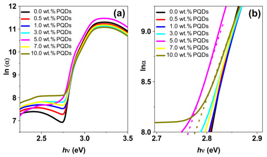
Figure 5.
(a) Logarithm of the absorption coefficients and (b) magnification of the MEH–PPV/PFO hybrid, CsPbBr3-PQDs, and PQDs/(MEH–PPV/PFO) composite thin films as a function of the photon energy.
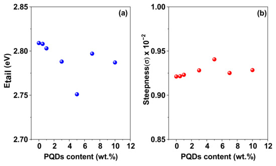
Figure 6.
(a) Variations in the Urbach energy (Eu) and (b) the steepness parameter of the MEH−PPV/PFO hybrid, CsPbBr3−PQDs, and PQDs/(MEH−PPV/PFO) composite thin-films as a function of the PQDs content. The solid lines represent data−fitting.
Analysis revealed that the Eu gradually decreased from 2.810 to 2.750 eV when the PQDs content in the hybrid increased. This decrease could be attributed to the variations in the defect density and crystallites’ sizes observed during XRD analysis. In other words, larger Eu values are representative of increased compositional, topological, or structural disorder [37,38]. However, the values observed in our study indicated that there was less compositional and structural disorder in the hybrid composites relative to their MEH–PPV/PFO counterparts [37,38].
Depending on the photon energy and the prevailing temperature, the steepness parameter (σ) of the Urbach tail can be calculated using the following equation [36]:
where kβ is the Boltzmann constant, and T is the absolute temperature. This equation describes the shrinkage/broadening of the optical absorption edge due to interactions between electrons and/or excitons and the optical phonons in semiconductors, resulting in the Urbach effect. The dependence of the steepness parameter on the PQDs content in the composite thin films at room temperature is shown in Figure 6b. Here, a decrease in the Eu value or an increase in the σ upon incremental addition of the CsPbBr3-QDs was attributed to a decrease in the localized density of the electronic states within the forbidden bandgap of the hybrids [28,39].
σ = kβT/Eu
If the k-vector (momentum) of the minimal energy state in the CB and the maximal energy state in the VB are the same, the bandgap is defined as a “direct gap” transition. However, if they are different, the bandgap is defined as an “indirect gap” transition [37]. It is possible to determine the direct and indirect transitions in the bandgap of the material, and ultimately, the structure of the material’s electronic band, by analyzing the optical absorption spectra [40,41]:
where C is a constant that depends on the transition probability, Eg is the energy bandgap, and n represents the nature of the transition, namely, n = 2 and 1/2 for direct and indirect bandgaps, respectively. The existence of both direct and indirect bandgap types was confirmed via linearity in the plot of (αhν)2 and (αhν)1/2 versus the photon energy (hν), as shown in Figure 7a,b, respectively. Here, the extrapolation of the linear portion of the plot to α = 0 resulted in the corresponding bandgap. Both the direct and indirect bandgaps were between 2.8 and 3.0 eV (from Figure 7a,b), and the values obtained were plotted in Figure 7c,d, respectively.
(αhν)n = C(hν − Eg)
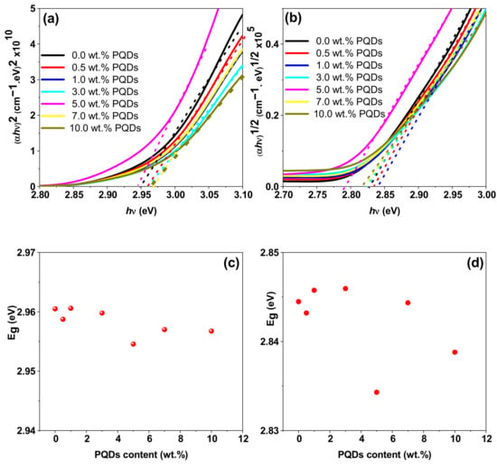
Figure 7.
(a) Plots of (αhν)2 vs. (hν) and (b) (αhν)1/2 vs. (hν). (c,d) are variations in the direct and indirect optical bandgaps of the MEH−PPV/PFO hybrid, respectively, as a function of the PQDs content.
We determined that the optical bandgap was weakly dependent on the PQDs content, as noted by the slight decrease in the direct (indirect) bandgaps from 2.961 (2.847) to 2.957 (2.839) eV.
The existence of both direct and indirect bandgaps in the PQDs/(MEH–PPV/PFO) composite films increased the range of the absorption energy, thereby improving the efficiency of photoelectric energy conversion processes [42]. The reduction in the bandgap with incrementally higher PQDs content in the hybrid could be interpreted as an increase in the disorder degree in the structure of the hybrid, resulting in raising the concentration of localized energy levels.
A strong correlation between the Eu and Eg values was observed in the spectral shift that occurred after the incorporation of the CsPbBr3-QDs. This correlation showed that the transitions across the bandgap and the transitions responsible for the Urbach edge are both electronic transitions, which has been the main focus of previous publications [28,43].
The fluorescence spectra of the PQDs, the MEH–PPV/PFO blend, and the PQDs/(MEH–PPV/PFO) composite thin films are shown in Figure 8. Three peaks for PFO were detected at 435, 461, and 494 nm, which can be attributed to 0–0, 0–1, and 0–2 vibronic transitions, respectively.
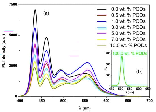
Figure 8.
Photoluminescence (PL) spectra of the MEH–PPV/PFO hybrid containing various PQDs weight ratios (a). The inset is the PL spectrum of the pristine PQDs (b).
Additionally, one peak at 507 nm and shoulder at 551 nm were observed for the PQDs and MEH-PPV, respectively. All these peaks were magnified in Figure 9 for more clarity.
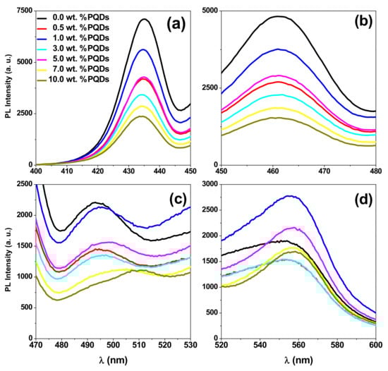
Figure 9.
PL spectra of the PQDs/(MEH–PPV/PFO) composite thin films in several ranges (a–d) for clarity.
A gradual decrease in the three emission peaks of the PFO (as summarized in Figure 10) upon increasing the PQDs content was observed, confirming the possibility of non-radiative energy transfer from PFO to PQDs in the ternary blend [18].
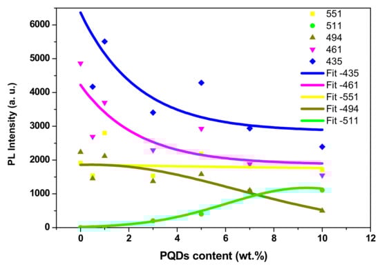
Figure 10.
PL intensity of the MEH–PPV/PFO hybrid as a function of the PQDs content at 435, 461, 494, 511, and 551 nm.
On the other hand, a gradual red-shift in the peak at 494 nm (Figure 9c) indicates an increase in the conjugation length of the donor (PFO), as discussed in previous works [18,44]. Moreover, the addition of more PQDs resulted in enhancing the peak at 551 nm with a gradual red-shifting. This finding confirms the possibility of non-radiative energy transfer from both PFO and PQDs to the MEH-PPV, since there is no significant emission for MEH-PPV at excitation at 350 nm [20]. Meanwhile, the enhancement intensity of the emission peak of the PQDs in the ternary blend, compared to pure PQDs, also confirms the efficiency of the non-radiative energy transfer from PFO to the PQDs in the ternary blend. This theory of non-radiative energy transfer was also confirmed by the significant overlap observed between the absorption spectra of PQDs and the fluorescence spectra of the MEH–PPV/PFO conjugated polymers, as shown in Figure 11.
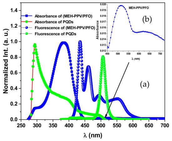
Figure 11.
PL and absorption normalized spectra of the MEH–PPV/PFO hybrid and CsPbBr3-PQDs thin films as a function of wavelength (a). The inset is the absorbance of MEH-PPV/PFO in the range 450–700 nm (b).
The efficient of non-radiative energy transfer (Förster resonant energy transfer) from both PFO and PQDs to MEH-PPV and from PFO to PQDs in the ternary blend were proved in our recent report [45]. In the future, polymer hybrids that possess a smooth surface and can undergo considerable non-radiative energy transfers will play a vital role in the development and optimization of optoelectronic devices.
4. Conclusions
In summary, hybrid thin films composed of PQDs/(MEH–PPV/PFO) conjugated polymers were successfully prepared by incorporating PQDs with various weight ratios via a solution blending method. The incorporation of the PQDs resulted in an increase in the grain size and reduction in both the dislocation density and lattice strain of the hybrid thin films. A weak dependence of direct and indirect optical bandgaps was observed in the MEH–PPV/PFO hybrid when the PQDs content increased, as evidenced by the slight decrease from 2.961 to 2.957 eV and from 2.847 to 2.839 eV for direct and indirect optical bandgaps, respectively. Consequently, an increase in the degree of disorder in the composite’s structure and the low concentration of the localized energy levels were observed, resulting in a dramatic increase in the roughness of the hybrid thin film. Moreover, the incremental increase in the PQDs content of the hybrids enhanced the non-radiative energy transfer processes. Employing these hybrids as emissive layers in optoelectronic devices can improve their performance significantly.
Author Contributions
Conceptualization, S.M.H.Q. and B.A.A.-A.; methodology, S.M.H.Q. and B.A.A.-A.; software, S.M.H.Q.; validation, S.M.H.Q., B.A.A.-A. and A.S.A.; formal analysis, S.M.H.Q. and B.A.A.-A.; investigation, S.M.H.Q., B.A.A.-A., H.M.G. and A.S.A.; resources, S.M.H.Q. and B.A.A.-A.; data curation, S.M.H.Q. and B.A.A.-A.; writing—original draft preparation, S.M.H.Q.; writing—review and editing, B.A.A.-A.; visualization, S.M.H.Q., and B.A.A.-A.; supervision, B.A.A.-A.; project administration, S.M.H.Q. and B.A.A.-A.; funding acquisition, S.M.H.Q. and B.A.A.-A. All authors have read and agreed to the published version of the manuscript.
Funding
This research received no external funding.
Institutional Review Board Statement
Not applicable.
Informed Consent Statement
Not applicable.
Data Availability Statement
Data is contained within the article.
Acknowledgments
The authors thank the Deanship of Scientific Research at King Saud University for funding this work through Research Group No. RG-1440-037.
Conflicts of Interest
The authors declare no conflict of interest.
References
- Longo, G.; Pertegás, A.; Martínez-Sarti, L.; Sessolo, M.; Bolink, H.J. Highly luminescent perovskite-aluminum oxide composites. J. Mater. Chem. C 2015, 3, 11286–11289. [Google Scholar] [CrossRef]
- Li, G.; Tan, Z.K.; Di, D.; Lai, M.L.; Jiang, L.; Lim, J.H.W.; Friend, R.H.; Greenham, N.C. Efficient Light-Emitting Diodes Based on Nanocrystalline Perovskite in a Dielectric Polymer Matrix. Nano Lett. 2015, 15, 2640–2644. [Google Scholar] [CrossRef]
- Yao, E.P.; Yang, Z.; Meng, L.; Sun, P.; Dong, S.; Yang, Y.; Yang, Y. High-Brightness Blue and White LEDs based on Inorganic Perovskite Nanocrystals and their Composites. Adv. Mater. 2017, 29, 1606859. [Google Scholar] [CrossRef] [PubMed]
- Xin, Y.; Zhao, H.; Zhang, J. Highly Stable and Luminescent Perovskite-Polymer Composites from a Convenient and Universal Strategy. ACS Appl. Mater. Interfaces 2018, 10, 4971–4980. [Google Scholar] [CrossRef] [PubMed]
- Wang, Y.; He, J.; Chen, H.; Chen, J.; Zhu, R.; Ma, P.; Towers, A.; Lin, Y.; Gesquiere, A.J.; Wu, S.T.; et al. Ultrastable, Highly Luminescent Organic-Inorganic Perovskite-Polymer Composite Films. Adv. Mater. 2016, 28, 10710–10717. [Google Scholar] [CrossRef]
- Zhang, Y.; Liu, J.; Wang, Z.; Xue, Y.; Ou, Q.; Polavarapu, L.; Zheng, J.; Qi, X.; Bao, Q. Synthesis, properties, and optical applications of low-dimensional perovskites. Chem. Commun. 2016, 52, 13637–13655. [Google Scholar] [CrossRef]
- Zhuo, Z.; Wu, X.; Yang, J. Two-dimensional silicon crystals with sizable band gaps and ultrahigh carrier mobility. Nanoscale 2018, 10, 1265–1271. [Google Scholar] [CrossRef]
- Tauc, J.; Grigorovici, R.; Vancu, A. Optical Properties and Electronic Structure of Amorphous Germanium. Phys. Status Solidi 1966, 15, 627–637. [Google Scholar] [CrossRef]
- Dou, L.; Liu, Y.; Hong, Z.; Li, G.; Yang, Y. Low-Bandgap Near-IR Conjugated Polymers/Molecules for Organic Electronics. Chem. Rev. 2015, 115, 12633–12665. [Google Scholar] [CrossRef]
- You, J.; Dou, L.; Yoshimura, K.; Kato, T.; Ohya, K.; Moriarty, T.; Emery, K.; Chen, C.C.; Gao, J.; Li, G.; et al. A polymer tandem solar cell with 10.6% power conversion efficiency. Nat. Commun. 2013, 4, 1446. [Google Scholar] [CrossRef]
- Zuo, C.; Ding, L. Bulk heterojunctions push the photoresponse of perovskite solar cells to 970 nm. J. Mater. Chem. A 2015, 3, 9063–9066. [Google Scholar] [CrossRef]
- Liu, Y.; Hong, Z.; Chen, Q.; Chang, W.; Zhou, H.; Song, T.B.; Young, E.; Yang, Y.; You, J.; Li, G.; et al. Integrated perovskite/bulk-heterojunction toward efficient solar cells. Nano Lett. 2015, 15, 662–668. [Google Scholar] [CrossRef] [PubMed]
- Han, G.S.; Yoo, J.S.; Yu, F.; Duff, M.L.; Kang, B.K.; Lee, J.K. Highly stable perovskite solar cells in humid and hot environment. J. Mater. Chem. A 2017, 5, 14733–14740. [Google Scholar] [CrossRef]
- Qaid, S.M.H.; Ghaithan, H.M.; Al-Asbahi, B.A.; Aldwayyan, A.S. Ultra-Stable Polycrystalline CsPbBr3 Perovskite–Polymer Composite Thin Disk for Light-Emitting Applications. Nanomaterials 2020, 10, 2382. [Google Scholar] [CrossRef] [PubMed]
- Christians, J.A.; Fung, R.C.M.; Kamat, P.V. An inorganic hole conductor for Organo-lead halide perovskite solar cells. improved hole conductivity with copper iodide. J. Am. Chem. Soc. 2014, 136, 758–764. [Google Scholar] [CrossRef]
- Qiu, L.; Ono, L.K.; Jiang, Y.; Leyden, M.R.; Raga, S.R.; Wang, S.; Qi, Y. Engineering Interface Structure to Improve Efficiency and Stability of Organometal Halide Perovskite Solar Cells. J. Phys. Chem. B 2018, 122, 511–520. [Google Scholar] [CrossRef]
- Qaid, S.M.H.; Ghaithan, H.M.; Al-Asbahi, B.A.; Aldwayyan, A.S. Single-Source Thermal Evaporation Growth and the Tuning Surface Passivation Layer Thickness Effect in Enhanced Amplified Spontaneous Emission Properties of CsPb(Br0.5Cl0.5)3 Perovskite Films. Polymers (Basel) 2020, 12, 2953. [Google Scholar] [CrossRef]
- Qaid, S.M.H.; Al-Asbahi, B.A.; Ghaithan, H.M.; AlSalhi, M.S.; Al dwayyan, A.S. Optical and structural properties of CsPbBr3 perovskite quantum dots/PFO polymer composite thin films. J. Colloid Interface Sci. 2020, 563, 426–434. [Google Scholar] [CrossRef]
- Al-asbahi, B.A. Influence of SiO2/TiO2 Nanocomposite on the Optoelectronic Properties of PFO/MEH-PPV-Based OLED Devices. Polymers 2018, 10, 800. [Google Scholar] [CrossRef]
- Al-Asbahi, B.A.; Qaid, S.M.H.; Mohammad, M.H.; AlSalhi, M.S.; Aldwayyan, A.S. Long-range dipole–dipole energy transfer enhancement via addition of SiO2/TiO2 nanocomposite in PFO/MEH-PPV hybrid thin films. J. Appl. Polym. Sci. 2019, 136, 47845. [Google Scholar] [CrossRef]
- Qaid, S.M.H.; Khan, M.N.; Alqasem, A.; Hezam, M.; Aldwayyan, A. Restraining effect of film thickness on the behaviour of amplified spontaneous emission from methylammonium lead iodide perovskite. IET Optoelectron. 2018, 13, 2–6. [Google Scholar] [CrossRef]
- Optik, S.; Nipis, F.; Poli, N.; Sio, A. Optical Properties of Poly(9,9′-di-n-octylfluorenyl-2.7-diyl)/Amorphous SiO2 Nanocomposite Thin Films. Sains Malays. 2013, 42, 1151–1157. [Google Scholar]
- Mansoor Ali, S.; Kayani, A.; Al Garawi, M.S.; Al-Ghamdi, S.S.; Al-Salman, S.A.; Baig, M.R.; Alkhuraiji, T.S. Observation of nano sized particles in proton irradiated pm-355 polymer with x-ray diffraction (XRD) and morphological studies. Dig. J. Nanomater. Biostruct. 2017, 12, 727–732. [Google Scholar]
- Aziz, S.B.; Hamsan, M.H.; Kadir, M.F.Z.; Karim, W.O.; Abdullah, R.M. Development of polymer blend electrolyte membranes based on chitosan: Dextran with high ion transport properties for EDLC application. Int. J. Mol. Sci. 2019, 20, 3369. [Google Scholar] [CrossRef]
- Aziz, S.B.; Abidin, Z.H.Z.; Arof, A.K. Effect of silver nanoparticles on the DC conductivity in chitosansilver triflate polymer electrolyte. Phys. B Condens. Matter 2010, 405, 4429–4433. [Google Scholar] [CrossRef]
- Beal, R.E.; Slotcavage, D.J.; Leijtens, T.; Bowring, A.R.; Belisle, R.A.; Nguyen, W.H.; Burkhard, G.F.; Hoke, E.T.; McGehee, M.D. Cesium Lead Halide Perovskites with Improved Stability for Tandem Solar Cells. J. Phys. Chem. Lett. 2016, 7, 746–751. [Google Scholar] [CrossRef]
- Li, C.; Zang, Z.; Han, C.; Hu, Z.; Tang, X.; Du, J.; Leng, Y.; Sun, K. Enhanced random lasing emission from highly compact CsPbBr3 perovskite thin films decorated by ZnO nanoparticles. Nano Energy 2017, 40, 195–202. [Google Scholar] [CrossRef]
- Keshav, R.; Padiyar, M.; Meghana, N.; Mahesha, M.G. Analysis of PV deposited ZnTe thin films through Urbach tail and photoluminescence spectroscopy. J. Lumin. 2018, 194, 257–263. [Google Scholar] [CrossRef]
- Thompson, C.V.; Carel, R. Stress and grain growth in thin films. J. Mech. Phys. Solids 1996, 44, 657–673. [Google Scholar] [CrossRef]
- Hung, H.W.; Yokoyama, N.; Yahiro, M.; Adachi, C. Low driving voltage organic light emitting diode using phenanthrene oligomers as electron transport layer. Thin Solid Films 2008, 516, 8717–8720. [Google Scholar] [CrossRef]
- Li, F.; Tang, H.; Shinar, J.; Resto, O.; Weisz, S.Z. Effects of aquaregia treatment of indium-tin-oxide substrates on the behavior of double layered organic light-emitting diodes. Appl. Phys. Lett. 1997, 70, 2741–2743. [Google Scholar] [CrossRef]
- Al-Asbahi, B.A.; Jumali, M.H.H.; AlSalhi, M.S. Enhanced optoelectronic properties of PFO/Fluorol 7GA hybrid light emitting diodes via additions of TiO2 nanoparticles. Polymers (Basel) 2016, 8, 334. [Google Scholar] [CrossRef] [PubMed]
- Al-Asbahi, B.A.; Haji Jumali, M.H.; Yap, C.C.; Mat Salleh, M. Influence of TiO2 nanoparticles on enhancement of optoelectronic properties of PFO-based light emitting diode. J. Nanomater. 2013, 2013, 561534. [Google Scholar] [CrossRef]
- Yakuphanoglu, F.; Cukurovali, A.; Yilmaz, I. Refractive index and optical absorption properties of the complexes of a cyclobutane containing thiazolyl hydrazone ligand. Opt. Mater. (Amst) 2005, 27, 1363–1368. [Google Scholar] [CrossRef]
- Mebadi, A.; Houshmand, M.; Zandi, M.H.; Gorji, N.E. Simulations of the intermediate bandwidth fluctuations in nanostructured PV. Phys. E Low-Dimens. Syst. Nanostruct. 2013, 53, 130–136. [Google Scholar] [CrossRef]
- Hossain, M.S.; Kabir, H.; Rahman, M.M.; Hasan, K.; Bashar, M.S.; Rahman, M.; Gafur, M.A.; Islam, S.; Amri, A.; Jiang, Z.T.; et al. Understanding the shrinkage of optical absorption edges of nanostructured Cd-Zn sulphide films for photothermal applications. Appl. Surf. Sci. 2017, 392, 854–862. [Google Scholar] [CrossRef]
- Evingür, G.A.; Pekcan, Ö. Optical energy band gap of PAAm-GO composites. Compos. Struct. 2016, 183, 212–215. [Google Scholar] [CrossRef]
- Rawat, A.; Mahavar, H.K.; Chauhan, S.; Tanwar, A.; Singh, P.J. Optical band gap of polyvinylpyrrolidone/polyacrilamide blend thin films. Indian J. Pure Appl. Phys. 2012, 50, 100–104. [Google Scholar]
- Jumali, M.H.H.; Al-Asbahi, B.A.; Yap, C.C.; Salleh, M.M.; Alsalhi, M.S. Optoelectronic property enhancement of conjugated polymer in poly(9,9′-di-n-octylfluorenyl-2.7-diyl)/titania nanocomposites. Thin Solid Films 2012, 524, 257–262. [Google Scholar] [CrossRef]
- Al-Asbahi, B.A.; Qaid, S.M.H.; Hezam, M.; Bedja, I.; Ghaithan, H.M.; Aldwayyan, A.S. Effect of deposition method on the structural and optical properties of CH3NH3PbI3 perovskite thin films. Opt. Mater. 2020, 103, 109836. [Google Scholar]
- Yakuphanoglu, F.; Sekerci, M.; Ozturk, O.F. The determination of the optical constants of cu(ii) compound having 1-chloro-2,3-o-cyclohexylidinepropane thin film. Opt. Commun. 2004, 239, 275–280. [Google Scholar] [CrossRef]
- Chen, Y.H.; Ho, C.H. Temperature dependence of direct and indirect band gaps of Bi13I2S18 hexagonal rod crystals. Mater. Chem. Phys. 2018, 206, 71–75. [Google Scholar] [CrossRef]
- Tichy, L.; Ticha, H. Correlation between photo-induced red shift of the optical band gap and the slope of Urbach edge in amorphous and glassy As2S3. Mater. Lett. 2015, 164, 232–234. [Google Scholar] [CrossRef]
- Yahya, N.Z.; Rusop, M. Investigation on the Optical and Surface Morphology of Conjugated Polymer MEH-PPV: ZnO Nanocomposite Thin Films. J. Nanomater. 2012, 2012, 793679. [Google Scholar] [CrossRef]
- Al-Asbahi, B.A.; Qaid, S.M.H.; Ghaithan, H.M.; Aldwayyan, A.S. Triplet energy transfer mechanism of ternary organic hybrid thin films of PFO/MEH-PPV/CsPbBR3 perovskite quantum dots. Nanomaterials 2020, 10, 2094. [Google Scholar] [CrossRef]
Publisher’s Note: MDPI stays neutral with regard to jurisdictional claims in published maps and institutional affiliations. |
© 2021 by the authors. Licensee MDPI, Basel, Switzerland. This article is an open access article distributed under the terms and conditions of the Creative Commons Attribution (CC BY) license (http://creativecommons.org/licenses/by/4.0/).