

Effects of Polysilane Addition to Chlorobenzene and High Temperature Annealing on CH3NH3PbI3 Perovskite Photovoltaic Devices

 , , ,
, , ,
Abstract
:1. Introduction
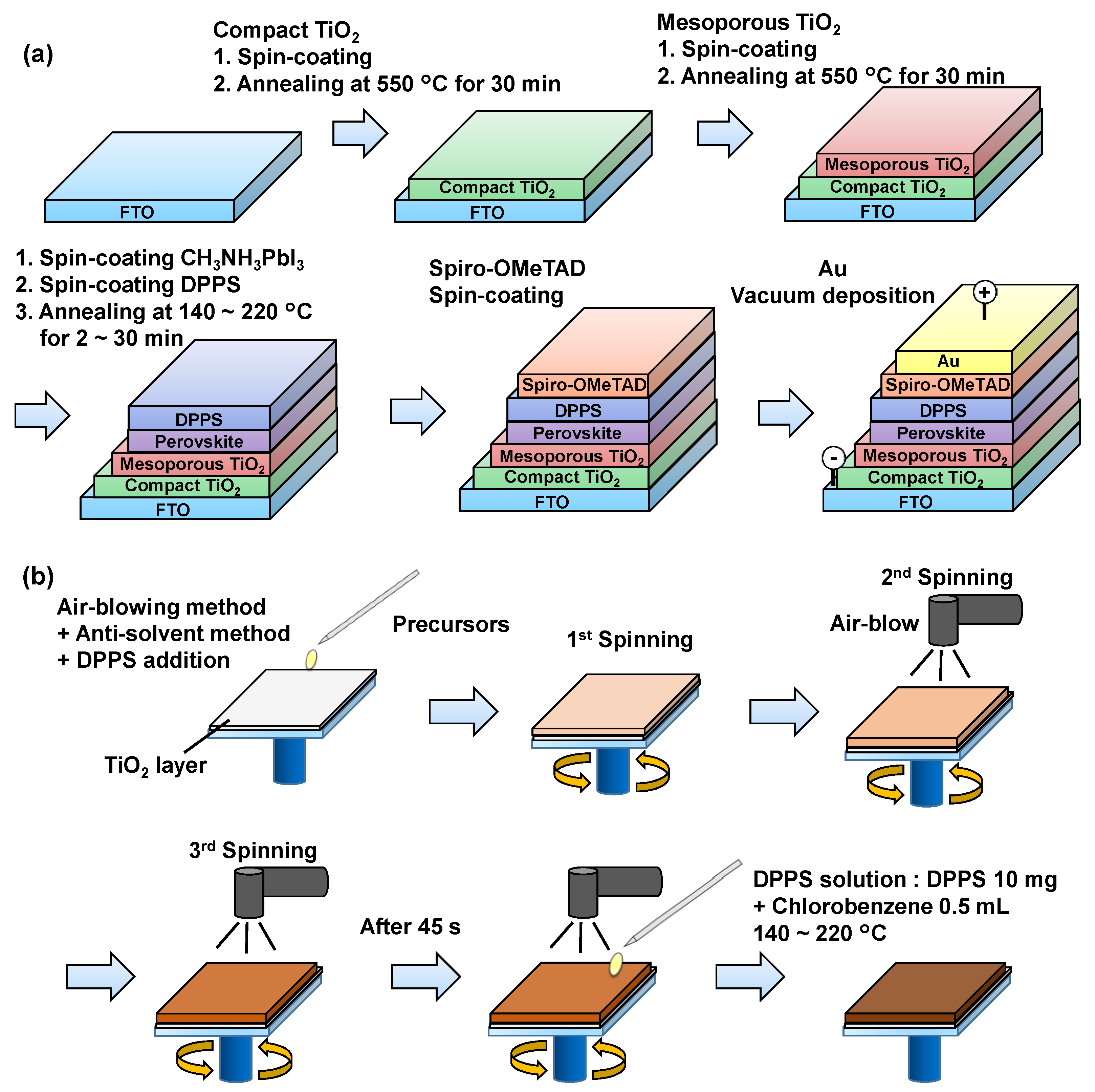
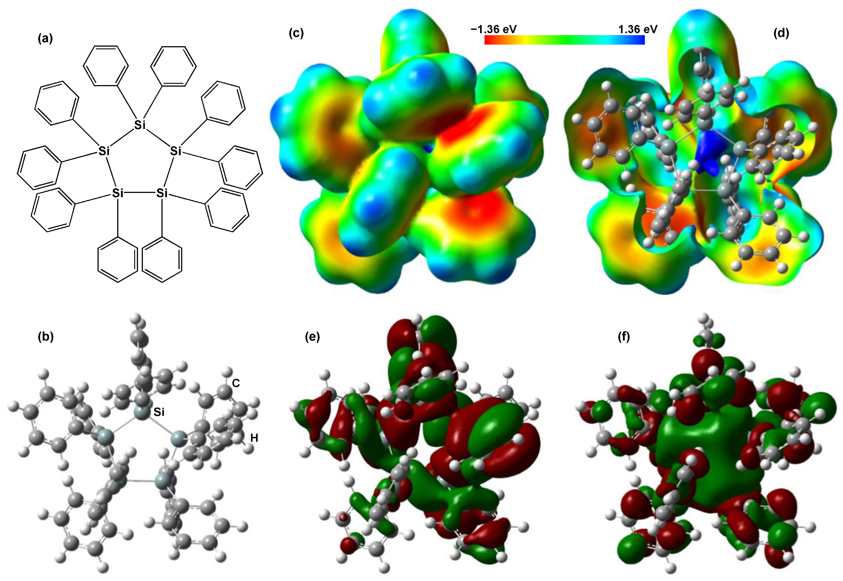
2. Experimental and Calculation Procedures
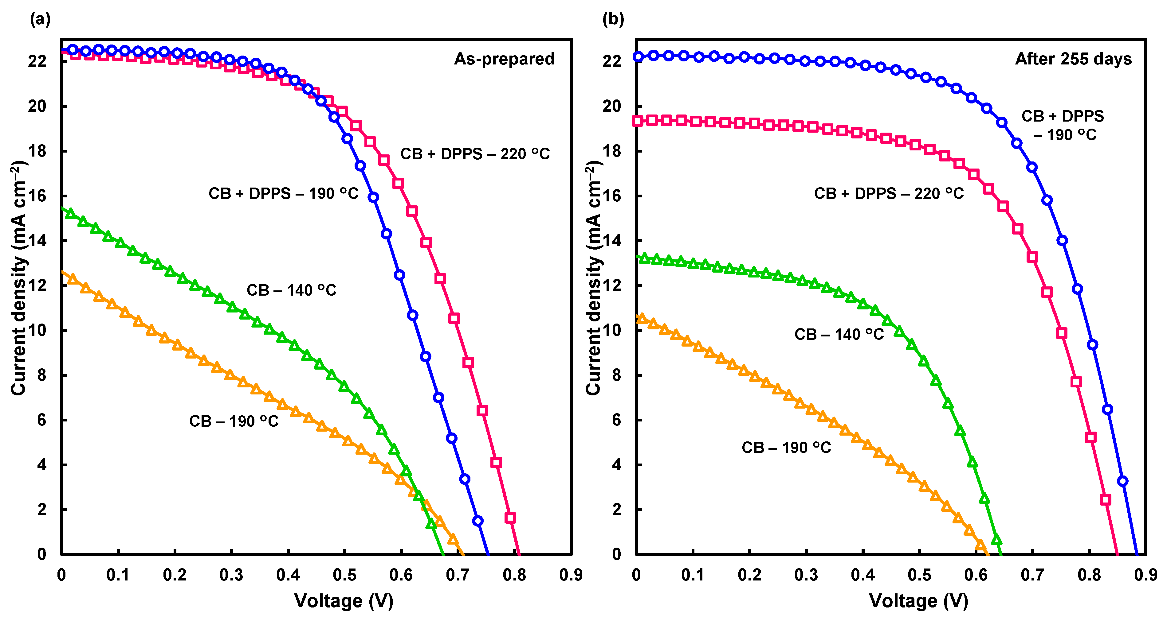
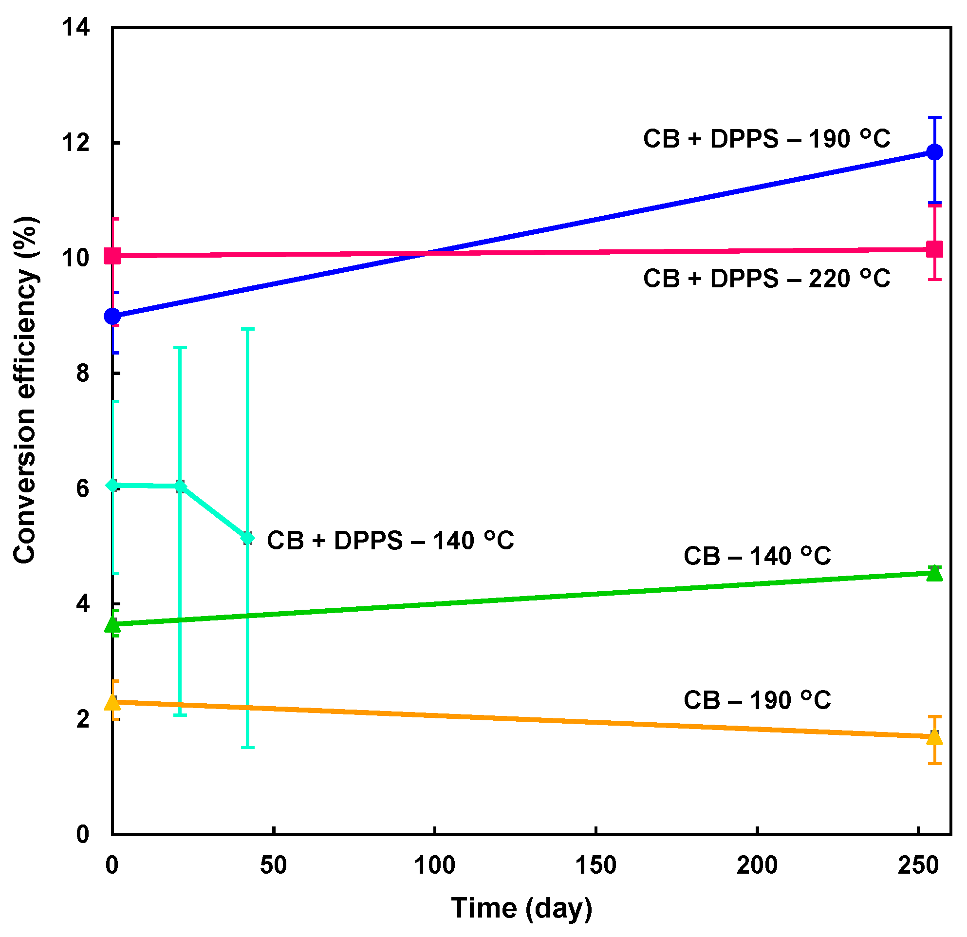
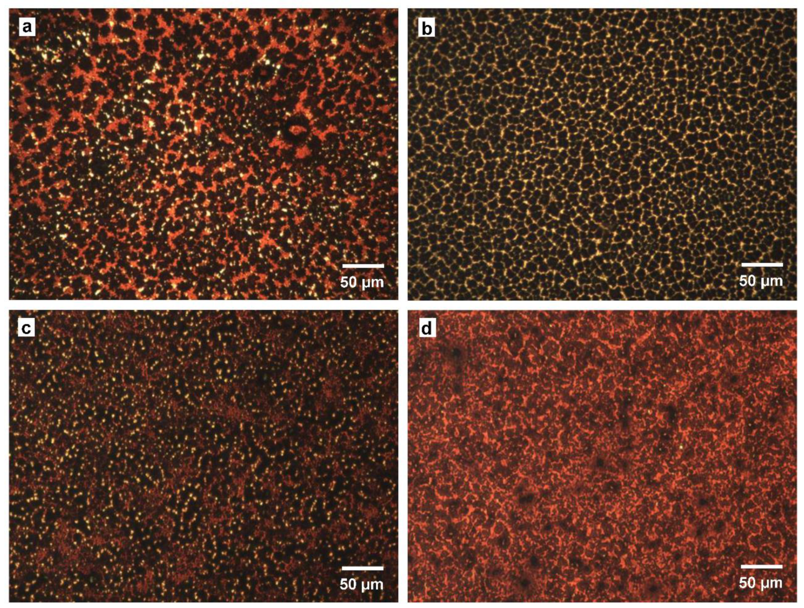
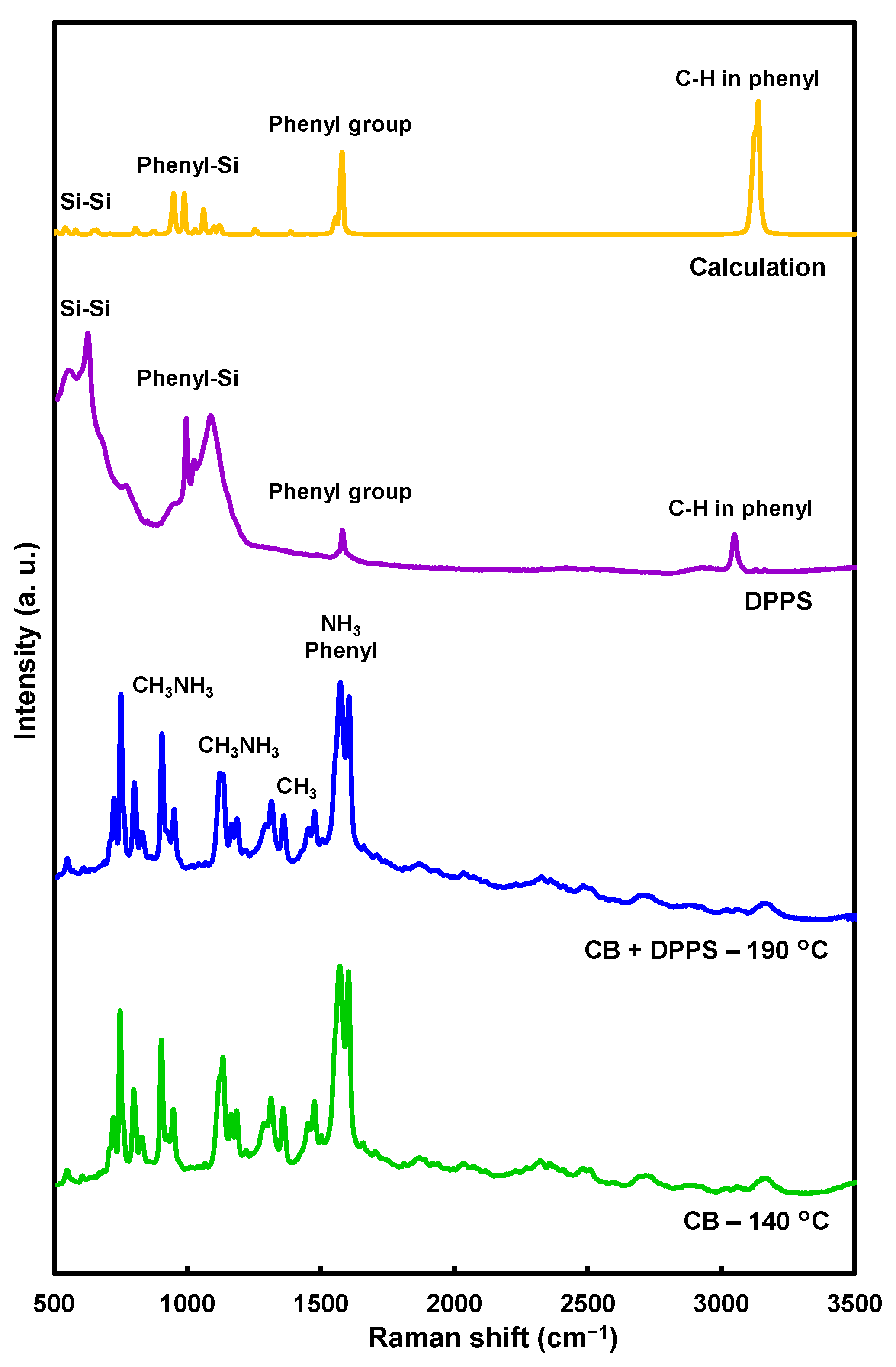
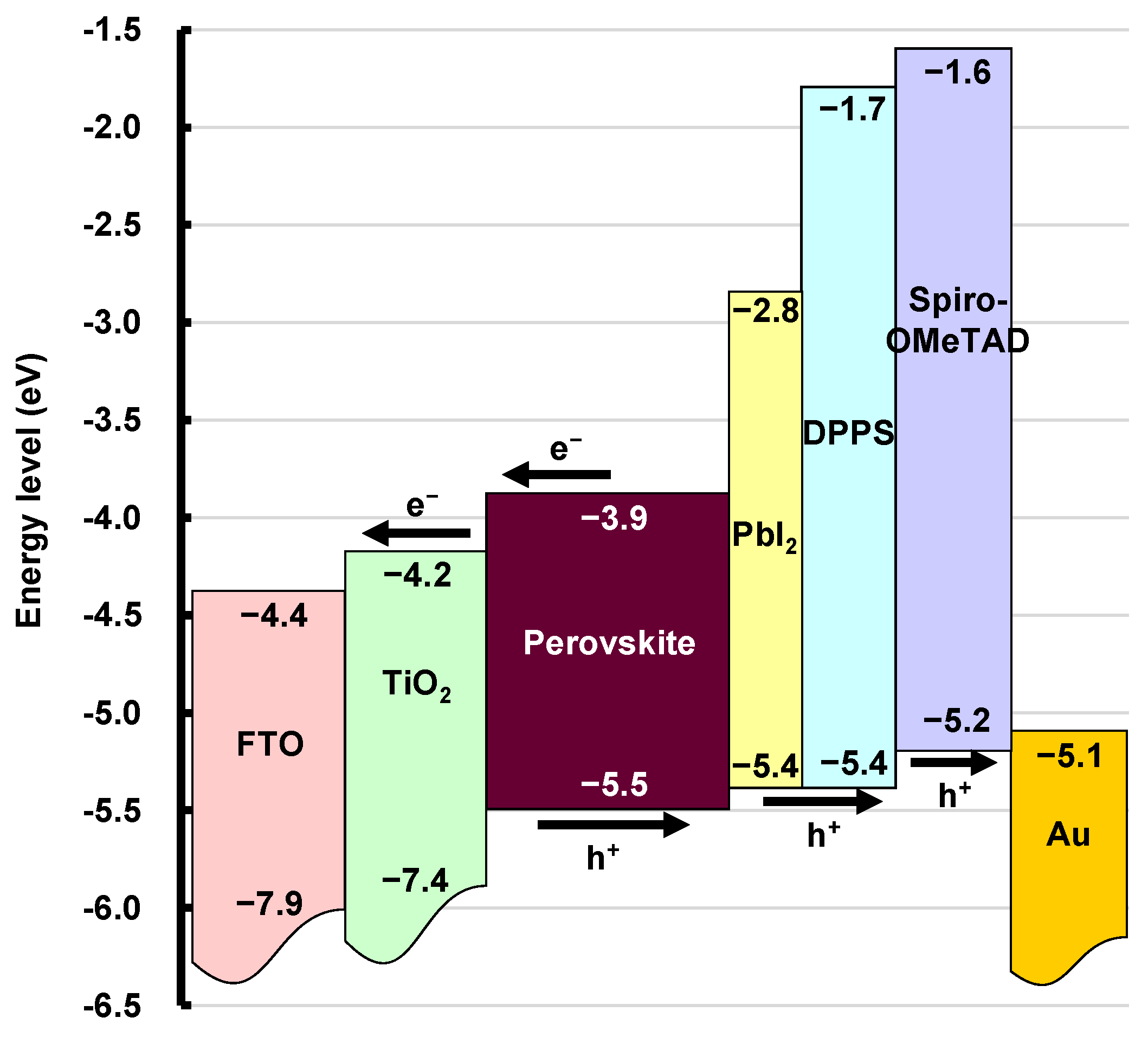
3. Results and Discussion
4. Conclusions
Author Contributions
Funding
Institutional Review Board Statement
Informed Consent Statement
Data Availability Statement
Conflicts of Interest
References
- Gedamu, D.; Asuo, I.M.; Benetti, D.; Basti, M.; Ka, I.; Cloutier, S.G.; Rosei, F.; Nechache, R. Solvent-antisolvent ambient processed large grain size perovskite thin films for high-performance solar cells. Sci. Rep. 2018, 8, 12885. [Google Scholar] [CrossRef] [PubMed]
- Mingyu, J.; Choi, I.W.; Go, E.M.; Cho, Y.; Kim, M.; Byongkyu, L.; Seonghun, J.; Yimhyun, J.; Choi, H.W.; Lee, J.; et al. Stable perovskite solar cells with efficiency exceeding 24.8% and 0.3-V voltage loss. Science 2020, 369, 1615–1620. [Google Scholar] [CrossRef]
- Miyasaka, T.; Kulkarni, A.; Kim, G.M.; Öz, S.; Jena, A.K. Perovskite solar cells: Can we go organic-free, lead-free, and dopant-free? Adv. Energy Mater. 2020, 10, 1902500. [Google Scholar] [CrossRef]
- Tong, J.; Song, Z.; Kim, D.M.; Chen, X.; Chen, C.; Palmstrom, A.F.; Ndione, P.F.; Reese, M.O.; Dunfield, S.P.; Reid, O.G.; et al. Carrier lifetimes of >1 μs in Sn-Pb perovskites enable efficient all-perovskite tandem solar cells. Science 2019, 364, 475–479. [Google Scholar] [CrossRef] [PubMed]
- Wang, F.; Yang, M.; Yang, S.; Qu, X.; Yang, L.; Fan, L.; Yang, J.; Rosei, F. Iodine-assisted antisolvent engineering for stable perovskite solar cells with efficiency >21.3%. Nano Energy 2020, 67, 104224. [Google Scholar] [CrossRef]
- Dunfield, S.P.; Bliss, L.; Zhang, F.; Luther, J.M.; Zhu, K.; van Hest, M.F.A.M.; Reese, M.O.; Berry, J.J. From defects to degradation: A mechanistic understanding of degradation in perovskite solar cell devices and modules. Adv. Energy Mater. 2020, 10, 1904054. [Google Scholar] [CrossRef]
- Lee, J.W.; Kim, S.G.; Yang, J.M.; Yang, Y.; Park, N.G. Verification and mitigation of ion migration in perovskite solar cells. APL Mater. 2019, 7, 041111. [Google Scholar] [CrossRef] [Green Version]
- Zhang, X.; Yin, J.; Nie, Z.; Zhang, Q.; Sui, N.; Chen, B.; Zhang, Y.; Qu, K.; Zhao, J.; Zhou, H. Lead-free and amorphous organic–inorganic hybrid materials for photovoltaic applications: Mesoscopic CH3NH3MnI3/TiO2 heterojunction. RSC Adv. 2017, 7, 37419–37425. [Google Scholar] [CrossRef] [Green Version]
- Dong, H.; Wu, Z.; Xi, J.; Xu, X.; Zuo, L.; Lei, T.; Zhao, X.; Zhang, L.; Hou, X. Pseudohalide-induced recrystallization engineering for CH3NH3PbI3 film and its application in highly efficient inverted planar heterojunction perovskite solar cells. Adv. Funct. Mater. 2017, 28, 1704836. [Google Scholar] [CrossRef]
- Oku, T. Crystal structures of perovskite halide compounds used for solar cells. Rev. Adv. Mater. Sci. 2020, 59, 264–305. [Google Scholar] [CrossRef]
- Travis, W.; Glover, E.N.K.; Bronstein, H.; Scanlon, D.O.; Palgrave, R.G. On the application of the tolerance factor to inorganic and hybrid halide perovskites: A revised system. Chem. Sci. 2016, 7, 4548–4556. [Google Scholar] [CrossRef] [Green Version]
- Hoefler, S.F.; Trimmel, G.; Rath, T. Progress on lead-free metal halide perovskites for photovoltaic applications: A review. Monatsh. Chem. 2017, 148, 795–826. [Google Scholar] [CrossRef] [PubMed] [Green Version]
- Tanaka, H.; Oku, T.; Ueoka, N. Structural stabilities of organic–inorganic perovskite crystals. Jpn. J. Appl. Phys. 2018, 57, 08RE12. [Google Scholar] [CrossRef]
- Zhou, Y.; Yang, M.; Pang, S.; Zhu, K.; Padture, N.P. Exceptional morphology-preserving evolution of formamidinium lead triiodide perovskite thin films via organic-cation displacement. J. Am. Chem. Soc. 2016, 138, 5535–5538. [Google Scholar] [CrossRef]
- Hu, M.; Liu, L.; Mei, A.; Yang, Y.; Liu, T.; Han, H. Efficient hole conductor-free, fully printable mesoscopic perovskite solar cells with a broad light harvester NH2CH=NH2PbI3. J. Mater. Chem. A 2014, 2, 17115–17121. [Google Scholar] [CrossRef]
- Suzuki, A.; Kato, M.; Ueoka, N.; Oku, T. Additive effect of formamidinium chloride in methylammonium lead halide compound-based perovskite solar cells. J. Electron. Mater. 2019, 48, 3900–3907. [Google Scholar] [CrossRef]
- Wang, Y.; Zhang, T.; Li, G.; Xu, F.; Li, Y.; Yang, Y.; Zhao, Y. A mixed-cation lead iodide MA1-xEAxPbI3 absorber for perovskite solar cells. J. Energy Chem. 2018, 27, 215–218. [Google Scholar] [CrossRef] [Green Version]
- Nishi, K.; Oku, T.; Kishimoto, T.; Ueoka, N.; Suzuki, A. Photovoltaic characteristics of CH3NH3PbI3 perovskite solar cells added with ethylammonium bromide and formamidinium iodide. Coatings 2020, 10, 410. [Google Scholar] [CrossRef] [Green Version]
- Jodlowski, A.D.; Roldán-Carmona, C.; Grancini, G.; Salado, M.; Ralaiarisoa, M.; Ahmad, S.; Koch, N.; Camacho, L.; Miguel, G.; Nazeeruddin, M. Large guanidinium cation mixed with methylammonium in lead iodide perovskites for 19% efficient solar cells. Nat. Energy 2017, 2, 972–979. [Google Scholar] [CrossRef] [Green Version]
- Kishimoto, T.; Suzuki, A.; Ueoka, N.; Oku, T. Effects of guanidinium addition to CH3NH3PbI3-xClx perovskite photovoltaic devices. J. Ceram. Soc. Jpn. 2019, 127, 491–497. [Google Scholar] [CrossRef] [Green Version]
- Suzuki, A.; Miyamoto, Y.; Oku, T. Electronic structures, spectroscopic properties, and thermodynamic characterization of sodium or potassium-incorporated CH3NH3PbI3 by first principles calculation. J. Mater. Sci. 2020, 55, 9728–9738. [Google Scholar] [CrossRef]
- Zheng, F.; Chen, W.; Bu, T.; Ghiggino, K.P.; Huang, F.; Cheng, Y.; Tapping, P.; Kee, T.W.; Jia, B.; Wen, X. Triggering the passivation effect of potassium doping in mixed-cation mixed-halide perovskite by light illumination. Adv. Energy Mater. 2019, 9, 1901016. [Google Scholar] [CrossRef]
- Machiba, H.; Oku, T.; Kishimoto, T.; Ueoka, N.; Suzuki, A. Fabrication and evaluation of K-doped MA0.8FA0.1K0.1PbI3(Cl) perovskite solar cells. Chem. Phys. Lett. 2019, 730, 117–123. [Google Scholar] [CrossRef]
- Kandori, S.; Oku, T.; Nishi, K.; Kishimoto, T.; Ueoka, N.; Suzuki, A. Fabrication and characterization of potassium- and formamidinium-added perovskite solar cells. J. Ceram. Soc. Jpn. 2020, 128, 805–811. [Google Scholar] [CrossRef]
- Bush, K.A.; Frohna, K.; Prasanna, R.; Beal, R.E.; Leijtens, T.; Swifter, S.A.; McGehee, M.D. Compositional engineering for efficient wide band gap perovskites with improved stability to photoinduced phase segregation. ACS Energy Lett. 2018, 3, 428–435. [Google Scholar] [CrossRef]
- Liu, C.; Kong, W.; Li, W.; Chen, H.; Li, D.; Wang, W.; Xu, B.; Cheng, C.; Jen, A.K.Y. Enhanced stability and photovoltage for inverted perovskite solar cells via precursor engineering. J. Mater. Chem. A 2019, 7, 15880–15886. [Google Scholar] [CrossRef]
- Zhang, M.; Yun, J.S.; Ma, Q.; Zheng, J.; Lau, C.F.J.; Deng, X.; Kim, J.; Kim, D.; Seidel, J.; Green, M.A.; et al. High-efficiency rubidium-incorporated perovskite solar cells by gas quenching. ACS Energy Lett. 2017, 2, 438–444. [Google Scholar] [CrossRef]
- Turren-Cruz, S.H.; Saliba, M.; Mayer, M.T.; Juárez-Santiesteban, H.; Mathew, X.; Nienhaus, L.; Tress, W.; Erodici, M.P.; Sher, M.J.; Bawendi, M.G.; et al. Enhanced charge carrier mobility and lifetime suppress hysteresis and improve efficiency in planar perovskite solar cells. Energy Environ. Sci. 2018, 11, 78–86. [Google Scholar] [CrossRef]
- Ueoka, N.; Oku, T.; Suzuki, A. Additive effects of alkali metals on Cu-modified CH3NH3PbI3-δClδ photovoltaic devices. RSC Adv. 2019, 9, 24231–24240. [Google Scholar] [CrossRef] [Green Version]
- Ueoka, N.; Oku, T. Effects of co-addition of sodium chloride and copper(II) bromide to mixed-cation mixed-halide perovskite photovoltaic devices. ACS Appl. Energy Mater. 2020, 3, 7272–7283. [Google Scholar] [CrossRef]
- Ueoka, N.; Oku, T.; Suzuki, A. Effects of doping with Na, K, Rb, and formamidinium cations on (CH3NH3)0.99Rb0.01Pb0.99Cu0.01I3-x(Cl, Br)x perovskite photovoltaic cells. AIP Adv. 2020, 10, 125023. [Google Scholar] [CrossRef]
- Chen, Z.; Dong, Q.; Liu, Y.; Bao, C.; Fang, Y.; Lin, Y.; Tang, S.; Wang, Q.; Xiao, X.; Bai, Y.; et al. Thin single crystal perovskite solar cells to harvest below-bandgap light absorption. Nat. Commun. 2017, 8, 1–7. [Google Scholar] [CrossRef] [PubMed] [Green Version]
- Wang, F.; Shimazaki, A.; Yang, F.; Kanahashi, K.; Matsuki, K.; Miyauchi, Y.; Takenobu, T.; Wakamiya, A.; Murata, Y.; Matsuda, K. Highly efficient and stable perovskite solar cells by interfacial engineering using solution-processed polymer layer. J. Phys. Chem. C 2017, 121, 1562–1568. [Google Scholar] [CrossRef]
- Han, T.H.; Lee, J.W.; Choi, C.; Tan, S.; Lee, C.; Zhao, Y.; Dai, Z.; Marco, N.D.; Lee, S.J.; Bae, S.H.; et al. Perovskite-polymer composite cross-linker approach for highly-stable and efficient perovskite solar cells. Nat. Commun. 2019, 10, 520. [Google Scholar] [CrossRef] [PubMed] [Green Version]
- Kim, G.W.; Choi, H.; Kim, M.; Lee, J.; Son, S.Y.; Park, T. Hole transport materials in conventional structural (n–i–p) perovskite solar cells: From past to the future. Adv. Energy Mater. 2020, 10, 1903403. [Google Scholar] [CrossRef]
- Calió, L.; Kazim, S.; Grätzel, M.; Ahmad, S. Hole-transport materials for perovskite solar cells. Angew. Chem. Int. Ed. 2016, 55, 14522–14545. [Google Scholar] [CrossRef]
- Singh, R.; Singh, P.K.; Bhattacharya, B.; Rhee, H.-W. Review of current progress in inorganic hole-transport materials for perovskite solar cells. Appl. Mater. Today 2019, 14, 175–200. [Google Scholar] [CrossRef]
- Bi, D.; Yi, C.; Luo, J.; Decoppet, J.D.; Zhang, F.; Zakeeruddin, S.M.; Li, X.; Hagfeldt, A.; Gratzel, M. Polymer-templated nucleation and crystal growth of perovskite films for solar cells with efficiency greater than 21%. Nat. Energy 2016, 1, 16142. [Google Scholar] [CrossRef]
- Taguchi, M.; Suzuki, A.; Tanaka, H.; Oku, T. Fabrication and characterization of perovskite solar cells added with MnCl2, YCl3 or poly(methyl methacrylate). AIP Conf. Proc. 2018, 1929, 020012. [Google Scholar] [CrossRef] [Green Version]
- Taguchi, M.; Suzuki, A.; Ueoka, N.; Oku, T. Effects of poly(methyl methacrylate) addition to perovskite photovoltaic devices. AIP Conf. Proc. 2019, 2067, 020018. [Google Scholar] [CrossRef]
- Oku, T.; Nakagawa, J.; Iwase, M.; Kawashima, A.; Yoshida, K.; Suzuki, A.; Akiyama, T.; Tokumitsu, K.; Yamada, M.; Nakamura, M. Microstructures and photovoltaic properties of polysilane-based solar cells. Jpn. J. Appl. Phys. 2013, 52, 04CR07. [Google Scholar] [CrossRef] [Green Version]
- Nakagawa, J.; Oku, T.; Suzuki, A.; Akiyama, T.; Yamada, M.; Fukunishi, S.; Kohno, K. Effects of PBr3 addition to polysilane thin films on structures and photovoltaic properties. Green Sustain. Chem. 2017, 7, 20–34. [Google Scholar] [CrossRef] [Green Version]
- Shirahata, Y.; Yamamoto, Y.; Suzuki, A.; Oku, T.; Fukunishi, S.; Kohno, K. Effects of polysilane-doped spiro-OMeTAD hole transport layers on photovoltaic properties. Phys. Status Solidi A 2017, 214, 1600591. [Google Scholar] [CrossRef]
- Shirahata, Y.A.; Oku, T.; Fukunishi, S.; Kohno, K. Fabrication of perovskite-type photovoltaic devices with polysilane hole transport layers. Mater. Sci. Appl. 2017, 8, 209–222. [Google Scholar] [CrossRef] [Green Version]
- Oku, T.; Nomura, J.; Suzuki, A.; Tanaka, H.; Fukunishi, S.; Minami, S.; Tsukada, S. Fabrication and characterization of CH3NH3PbI3 perovskite solar cells added with polysilanes. Int. J. Photoenergy 2018, 8654963. [Google Scholar] [CrossRef] [Green Version]
- Taguchi, M.; Suzuki, A.; Oku, T.; Fukunishi, S.; Minami, S.; Okita, M. Effects of decaphenylcyclopentasilane addition on photovoltaic properties of perovskite solar cells. Coatings 2018, 8, 461. [Google Scholar] [CrossRef] [Green Version]
- Taguchi, M.; Suzuki, A.; Oku, T.; Ueoka, N.; Minami, S.; Okita, M. Effects of annealing temperature on decaphenylcyclopentasilane-inserted CH3NH3PbI3 perovskite solar cells. Chem. Phys. Lett. 2019, 737, 136822. [Google Scholar] [CrossRef]
- Oku, T.; Kandori, S.; Taguchi, M.; Suzuki, A.; Okita, M.; Minami, S.; Fukunishi, S.; Tachikawa, T. Polysilane-inserted methylammonium lead iodide perovskite solar cells doped with formamidinium and potassium. Energies 2020, 13, 4776. [Google Scholar] [CrossRef]
- Oku, T.; Zushi, M.; Imanishi, Y.; Suzuki, A.; Suzuki, K. Microstructures and photovoltaic properties of perovskite-type CH3NH3PbI3 compounds. Appl. Phys. Express 2014, 7, 121601. [Google Scholar] [CrossRef]
- Oku, T.; Ohishi, Y.; Ueoka, N. Highly (100)-oriented CH3NH3PbI3(Cl) perovskite solar cells prepared with NH4Cl using an air blow method. RSC Adv. 2018, 8, 10389–10395. [Google Scholar] [CrossRef] [Green Version]
- Oku, T.; Ohishi, Y.; Suzuki, A.; Miyazawa, Y. Effects of NH4Cl addition to perovskite CH3NH3PbI3 photovoltaic devices. J. Ceram. Soc. Jpn. 2017, 125, 303–307. [Google Scholar] [CrossRef] [Green Version]
- Ueoka, N.; Oku, T.; Tanaka, H.; Suzuki, A.; Sakamoto, H.; Yamada, M.; Minami, S.; Miyauchi, S.; Tsukada, S. Effects of PbI2 addition and TiO2 electron transport layers for perovskite solar cells. Jpn. J. Appl. Phys. 2018, 57, 08RE05. [Google Scholar] [CrossRef]
- Oku, T.; Ohishi, Y. Effects of annealing on CH3NH3PbI3(Cl) perovskite photovoltaic devices. J. Ceram. Soc. Jpn. 2018, 126, 56–60. [Google Scholar] [CrossRef] [Green Version]
- Suzuki, A.; Oku, T. Effects of transition metals incorporated into perovskite crystals on the electronic structures and magnetic properties by first-principles calculation. Heliyon 2018, 4, e00755. [Google Scholar] [CrossRef] [Green Version]
- Suzuki, A.; Oku, T. Effects of mixed-valence states of Eu-doped FAPbI3 perovskite crystals studied by first-principles calculation. Mater. Adv. 2021, 2. in press. [Google Scholar] [CrossRef]
- Chen, H.-W.; Sakai, N.; Ikegami, M.; Miyasaka, T. Emergence of hysteresis and transient ferroelectric response in organo-lead halide perovskite solar cells. J. Phys. Chem. Lett. 2014, 6, 164–169. [Google Scholar] [CrossRef]
- Pérez-Osorio, M.A.; Lin, Q.; Phillips, R.T.; Milot, R.L.; Herz, L.M.; Johnston, M.B.; Giustino, F. Raman spectrum of the organic–inorganic halide perovskite CH3NH3PbI3 from first principles and high-resolution low-temperature Raman measurements. J. Phys. Chem. C 2018, 122, 21703–21717. [Google Scholar] [CrossRef] [Green Version]
- Brivio, F.; Frost, J.M.; Skelton, J.M.; Jackson, A.J.; Weber, O.J.; Weller, M.T.; Goñi, A.R.; Leguy, A.M.A.; Barnes, P.R.F.; Walsh, A. Lattice dynamics and vibrational spectra of the orthorhombic, tetragonal, and cubic phases of methylammonium lead iodide. Phys. Rev. B 2015, 92, 144308. [Google Scholar] [CrossRef] [Green Version]
- Jeon, N.J.; Noh, J.H.; Kim, Y.C.; Yang, W.S.; Ryu, S.; Seok, S. Solvent engineering for high-performance inorganic–organic hybrid perovskite solar cells. Nat. Mater. 2014, 13, 897–903. [Google Scholar] [CrossRef] [PubMed]
- Xiao, M.; Huang, F.; Huang, W.; Dkhissi, Y.; Zhu, Y.; Etheridge, J.; Weale, A.G.; Bach, U.; Cheng, Y.B.; Spiccia, L. A fast deposition-crystallization procedure for highly efficient lead iodide perovskite thin-film solar cells. Angew. Chem. Int. Ed. 2014, 53, 9898–9903. [Google Scholar] [CrossRef] [PubMed]
- Tavakoli, M.M.; Yadav, P.; Prochowicz, D.; Sponseller, M.; Osherov, A.; Bulovic, V.; Kong, J. Controllable perovskite crystallization via antisolvent technique using chloride additives for highly efficient planar perovskite solar cells. Adv. Energy Mater. 2019, 9, 1803587. [Google Scholar] [CrossRef]
- Noh, J.H.; Im, S.H.; Heo, J.H.; Mandal, T.N.; Seok, S.I. Chemical management for colorful, efficient, and stable inorganic–organic hybrid nanostructured solar cells. Nano Lett. 2013, 13, 1764–1769. [Google Scholar] [CrossRef]
- Haga, Y.; Harada, Y. Photovoltaic characteristics of phthalocyanine-polysilane composite films. Jpn. J. Appl. Phys. 2001, 40, 855–861. [Google Scholar] [CrossRef]
- Chen, Q.; Zhou, H.; Song, T.B.; Luo, S.; Hong, Z.; Duan, H.S.; Dou, L.; Liu, Y.; Yang, Y. Controllable self-induced passivation of hybrid lead iodide perovskites toward high performance solar cells. Nano Lett. 2014, 14, 4158–4163. [Google Scholar] [CrossRef] [PubMed]
- Ueoka, N.; Oku, T. Stability characterization of PbI2-added CH3NH3PbI3−xClx photovoltaic devices. ACS Appl. Mater. Interfaces 2018, 10, 44443–44451. [Google Scholar] [CrossRef] [PubMed]
- Eames, C.; Frost, J.M.; Barnes, P.R.F.; O’Regan, B.C.; Walsh, A.; Islam, M.S. Ionic transport in hybrid lead iodide perovskite solar cells. Nat. Commun. 2015, 6, 7497. [Google Scholar] [CrossRef] [PubMed] [Green Version]


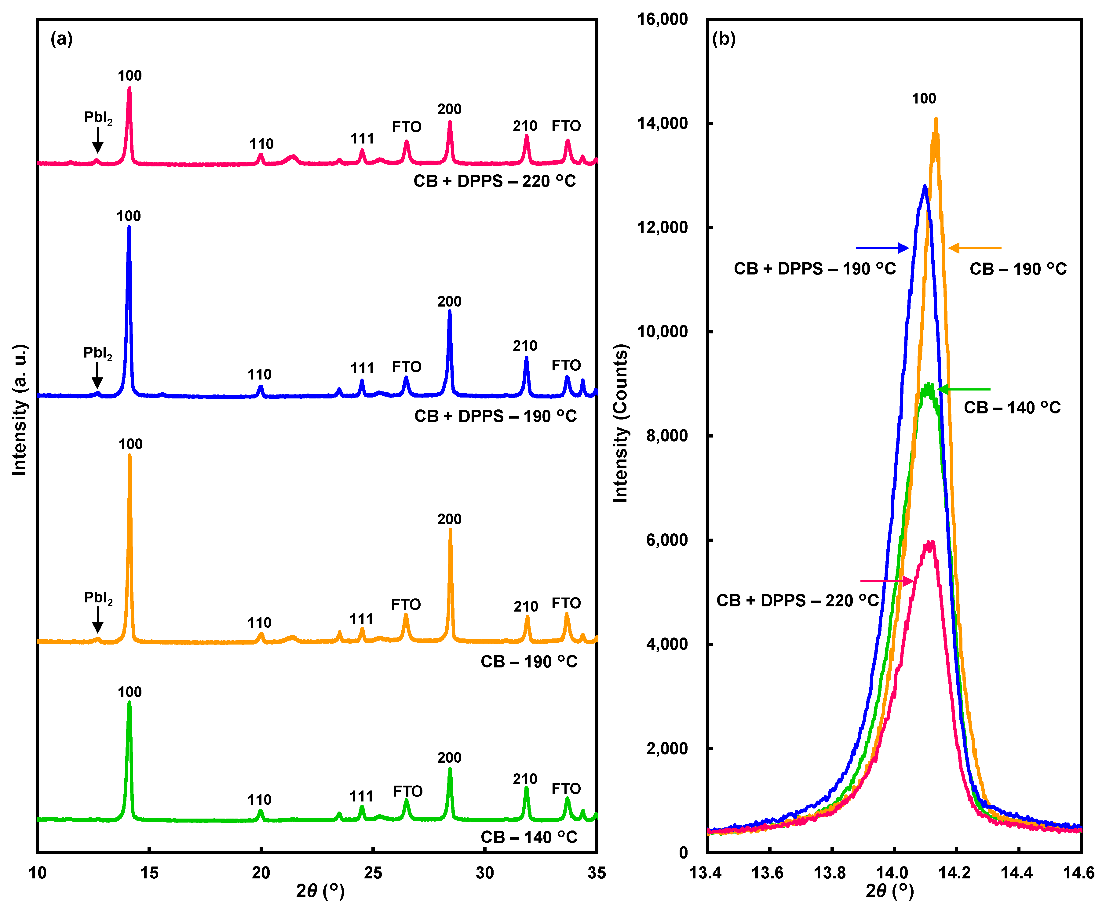
| Solution | Annealing (°C, min) | JSC (mA cm−2) | VOC (V) | FF | RS (Ω cm2) | RSh (Ω cm2) | η (%) | ηave (%) | HI |
|---|---|---|---|---|---|---|---|---|---|
| * | 100, 15 | 15.8 | 0.800 | 0.550 | 8.89 | 525 | 6.94 | 6.76 | 0.029 |
| CB | 140, 12 | 15.4 | 0.674 | 0.373 | 12.35 | 72 | 3.87 | 3.65 | −0.082 |
| CB | 190, 6 | 12.6 | 0.708 | 0.298 | 18.87 | 71 | 2.66 | 2.30 | −0.034 |
| CB + DPPS | 140, 60 | 12.6 | 0.903 | 0.660 | 8.13 | 916 | 7.51 | 6.06 | 0.076 |
| CB + DPPS | 190, 30 | 22.5 | 0.753 | 0.554 | 11.92 | 5670 | 9.40 | 8.99 | 0.334 |
| CB + DPPS | 220, 2 | 22.4 | 0.808 | 0.554 | 9.33 | 831 | 10.04 | 9.40 | 0.125 |
| CB + DPPS | 250, 1.5 | 20.5 | 0.875 | 0.524 | 9.90 | 268 | 9.40 | 8.71 | 0.043 |
| CB + DPPS | 260, 1 | 13.5 | 0.884 | 0.483 | 24.37 | 709 | 5.75 | 5.42 | 0.327 |
| After 255 days | - | - | - | - | - | - | - | - | - |
| CB | 140, 12 | 13.3 | 0.643 | 0.543 | 8.35 | 330 | 4.64 | 4.54 | 0.102 |
| CB | 190, 6 | 10.6 | 0.620 | 0.311 | 23.71 | 86 | 2.05 | 1.70 | −0.087 |
| CB + DPPS | 190, 30 | 22.2 | 0.884 | 0.634 | 7.35 | 5830 | 12.44 | 11.84 | 0.086 |
| CB + DPPS | 220, 2 | 19.3 | 0.849 | 0.618 | 8.03 | 2700 | 10.15 | 9.39 | 0.044 |
| Solution | Annealing (°C, min) | Lattice Constant a (Å) | Orientation I100/I210 |
|---|---|---|---|
| CB | 140, 12 | 6.270(0) | 3.6 |
| CB | 190, 6 | 6.265(1) | 7.5 |
| CB + DPPS | 190, 30 | 6.276(0) | 4.4 |
| CB + DPPS | 220, 2 | 6.270(1) | 2.7 |
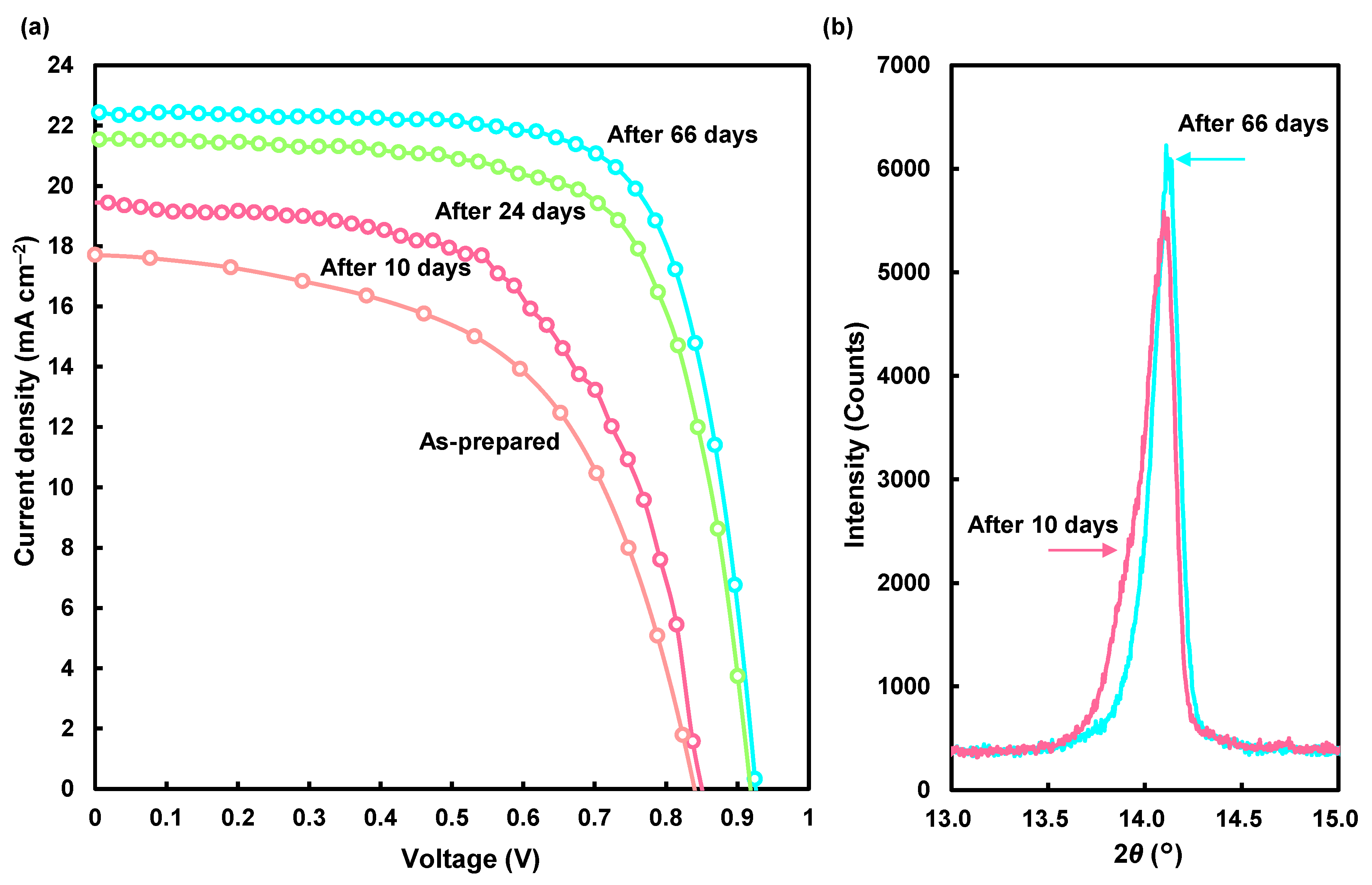
| Time (Day) | JSC (mA cm−2) | VOC (V) | FF | RS (Ω cm2) | RSh (Ω cm2) | η (%) | ηave (%) | HI |
|---|---|---|---|---|---|---|---|---|
| 0 | 17.7 | 0.839 | 0.558 | 4.41 | 908 | 8.30 | 6.58 | 0.268 |
| 10 | 19.4 | 0.850 | 0.593 | 3.49 | 1440 | 9.80 | 8.81 | 0.034 |
| 24 | 21.6 | 0.918 | 0.699 | 3.96 | 1610 | 13.82 | 12.48 | 0.046 |
| 58 | 22.3 | 0.930 | 0.724 | 3.66 | 2120 | 15.03 | 13.31 | 0.073 |
| 66 | 22.4 | 0.923 | 0.727 | 3.72 | 3070 | 15.10 | 13.38 | 0.085 |
| Time (Day) | Lattice Constant a (Å) | Orientation I100/I210 | Crystallite Size D100 (Å) |
|---|---|---|---|
| 10 | 6.272(1) | 1.9 | 486 |
| 66 | 6.268(1) | 2.6 | 617 |
Publisher’s Note: MDPI stays neutral with regard to jurisdictional claims in published maps and institutional affiliations. |
© 2021 by the authors. Licensee MDPI, Basel, Switzerland. This article is an open access article distributed under the terms and conditions of the Creative Commons Attribution (CC BY) license (https://creativecommons.org/licenses/by/4.0/).
Share and Cite
Oku, T.; Taguchi, M.; Suzuki, A.; Kitagawa, K.; Asakawa, Y.; Yoshida, S.; Okita, M.; Minami, S.; Fukunishi, S.; Tachikawa, T. Effects of Polysilane Addition to Chlorobenzene and High Temperature Annealing on CH3NH3PbI3 Perovskite Photovoltaic Devices. Coatings 2021, 11, 665. https://doi.org/10.3390/coatings11060665
Oku T, Taguchi M, Suzuki A, Kitagawa K, Asakawa Y, Yoshida S, Okita M, Minami S, Fukunishi S, Tachikawa T. Effects of Polysilane Addition to Chlorobenzene and High Temperature Annealing on CH3NH3PbI3 Perovskite Photovoltaic Devices. Coatings. 2021; 11(6):665. https://doi.org/10.3390/coatings11060665
Chicago/Turabian StyleOku, Takeo, Masaya Taguchi, Atsushi Suzuki, Kaede Kitagawa, Yugo Asakawa, Satoshi Yoshida, Masanobu Okita, Satoshi Minami, Sakiko Fukunishi, and Tomoharu Tachikawa. 2021. "Effects of Polysilane Addition to Chlorobenzene and High Temperature Annealing on CH3NH3PbI3 Perovskite Photovoltaic Devices" Coatings 11, no. 6: 665. https://doi.org/10.3390/coatings11060665
APA StyleOku, T., Taguchi, M., Suzuki, A., Kitagawa, K., Asakawa, Y., Yoshida, S., Okita, M., Minami, S., Fukunishi, S., & Tachikawa, T. (2021). Effects of Polysilane Addition to Chlorobenzene and High Temperature Annealing on CH3NH3PbI3 Perovskite Photovoltaic Devices. Coatings, 11(6), 665. https://doi.org/10.3390/coatings11060665