1. Introduction
Si and SiGe epitaxy can be performed using various techniques such as molecular beam epitaxy, low-pressure chemical vapor deposition (LPCVD), reduced-pressure chemical vapor deposition (RPCVD), and ultra-high vacuum chemical vapor deposition (UHVCVD). Currently, RPCVD is the most popular technique for Si and SiGe epitaxy; however, it requires a large amount of H
2 gas as the carrier gas. On the other hand, the epitaxial growth via UHVCVD is performed without a carrier gas, but the growth rate is limited, particularly at low temperatures, because the pressure is too low. High-order silanes are candidate Si precursors for low-temperature Si epitaxy due to the lower strength of the Si-Si bonds compared to the Si–H bonds. Previous studies have been conducted on high-order silane-based Si or SiGe epitaxy utilizing disilane [
1,
2], trisilane [
3,
4,
5,
6], tetrasilane [
7,
8], or neopentasilane [
9,
10]. However, these studies have focused on one or two high-order silanes compared to conventional precursors (silane; SiH
4 or dichlorosilane; SiCl
2H
2), and most were performed in RPCVD or LPCVD chambers with an abundance of ambient H
2 or N
2. Silane-based low-temperature CVD may also be applicable to the coating of sensing devices. For example, alkylsilane-based self-assembled monolayers (SAMs) deposited on metal oxides were suggested to replace expensive gold electrodes [
11]. Gabriunaite et al. demonstrated a transparent electrode system of octadecyltrichlorosilane-based SAM on fluorine-doped tin oxide (FTO) for biosensors [
12]; FTO can also be formed by using CVD techniques [
13]. In this study, we performed Si and SiGe epitaxy under UHVCVD (working pressure <0.1 mTorr) and LPCVD (working pressure 80 mTorr) conditions without a carrier gas. Various temperatures ranging from 400 to 650 °C were investigated using disilane, trisilane, and tetrasilane.
2. Experimental Procedure
First, we performed Si and SiGe epitaxy at 450 to 650 °C under UHVCVD conditions (<0.1 mTorr) on blanket Si (100) coupon wafers using a UHVCVD chamber (EURECA 3000, Jusung Engineering, Gwangju-si, Gyeonggi-do, Korea). The base pressure was maintained at a 5 × 10
−8 torr using a turbo-molecular pump (TMP) (Leybold, Köln, Germany). Graphite heaters were used to control the temperature. The working pressure was not identified precisely in these experiments due to the absence of a pressure controller, and the cold cathode gauge was automatically isolated during the process. However, the working pressure did not exceed 0.1 mTorr, which was the lower limit of the convectron gauge. All samples were dipped in dilute HF (1:100) for 1 min to remove the native oxides. Then, they were rinsed with deionized water prior to loading. Subsequently, the samples were loaded into the CVD chamber within 3 min to inhibit native oxide regrowth. In situ plasma cleaning was performed before the epitaxial growth process. SF
6 and Cl
2 gases were then used with Ar plasma for 60 s each. High-order silane and germane precursors were supplied during this process without a carrier gas. Trisilane and tetrasilane are liquid precursors at room temperature unlike disilane. However, their vapor pressures are sufficiently high for the use of a conventional gas delivery system with a heated gas line, even though the flow rate is limited to either tens of standard cubic centimeters per minute (sccm; for trisilane) or a few sccm (for tetrasilane). A similar delivery system was demonstrated by Hazbun [
7]. In the case of Si epitaxy, the deposition of the SiGe marker layer was preceded by Si epitaxial growth. This was used to easily determine the resulting thickness.
Si epitaxy was also carried out at a higher pressure of approximately 100 mTorr and temperatures below 500 °C. The sample preparation and in situ cleaning methods were the same as those mentioned above unless otherwise stated. After in situ plasma cleaning, TMP was turned down for 10 min and the epitaxial growth process was conducted. No carrier gas was used during this process.
The epilayers were evaluated using various analysis techniques. The thicknesses of the epilayers were measured using transmission electron microscopy (TEM) (JEOL, Tokyo, Japan). The Ge concentrations were extracted using high-resolution x-ray diffraction (HR-XRD) (Rigaku, Tokyo, Japan) and the results were confirmed by energy-dispersive X-ray spectroscopy (EDS) (JEOL, Tokyo, Japan) and spectroscopic ellipsometry (SE) (J.A. Woollam, Lincoln, NE, USA). We note that the Ge concentration calculated via XRD is incorrect when strain relaxation occurs. Therefore, the crystal quality was confirmed upon the evaluation of the Ge concentration using HR-XRD. The crystal quality was analyzed via TEM, and the surface roughness was measured using atomic force microscopy (AFM) (Park Systems, Suwon, Korea).
3. Results and Discussion
Disilane- and trisilane-based Si epitaxy were carried out at 500 to 650 °C under UHVCVD conditions below 0.1 mTorr. Tetrasilane was excluded due to the limitation of its low flow rate. SiGe marker layers of approximately 5 nm were inserted between the Si epilayers and the substrates because the epilayers may be indistinguishable from the substrate. The Si growth rate can be increased, particularly in thin films, if the Ge concentration of the marker layer is adequately high. This phenomenon occurs because surface Ge atoms can act as hydrogen desorption centers due to the lower strength of the Ge–H bond compared to that of the Si–H bond [
14]. Therefore, the Ge concentration of the SiGe marker should be sufficiently low and should be targeted at 10%. The growth rates of these epitaxial layers were similar regardless of the existence of the marker layer, as shown in
Supplementary Materials Figure S1. The difference in the growth rate was less than 3%. There were no evident defects such as stacking faults at the interface between the SiGe marker layer and the Si epilayer or substrate as shown in
Supplementary Materials Figure S2. Therefore, all Si epitaxy experiments were performed using SiGe marker layers for ease of evaluation.
The flow rates of the Si precursors (disilane and trisilane) were fixed at 20 sccm. The growth time was 1000 s at ≥550 °C and 4000 s below 550 °C.
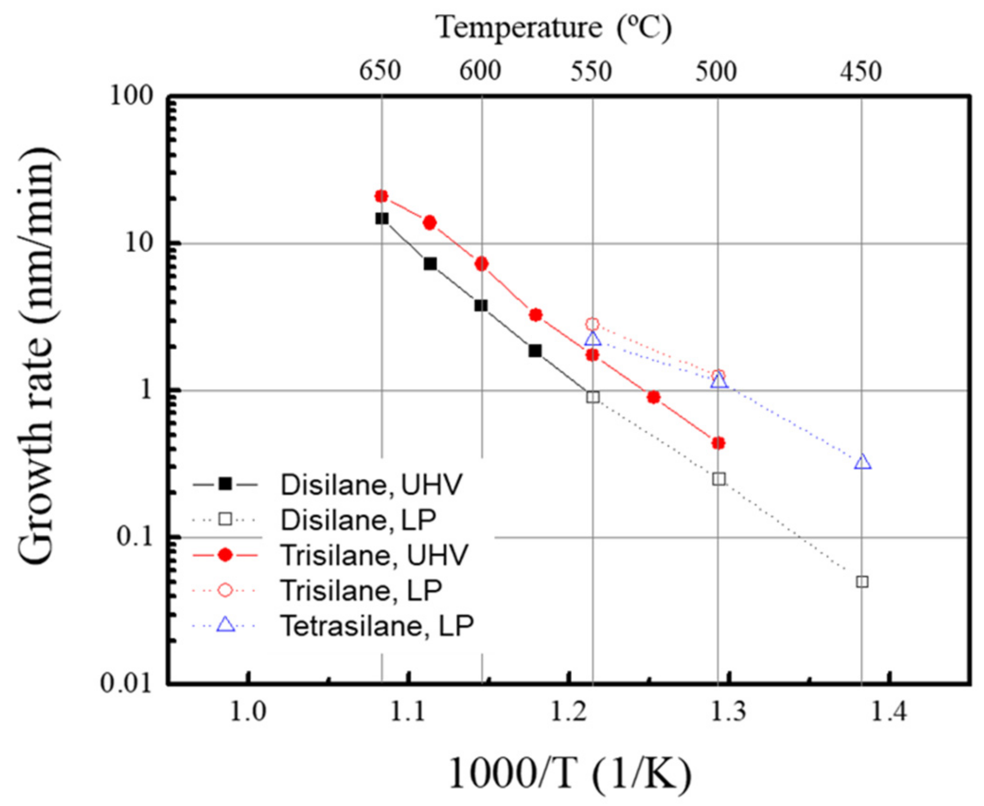
Figure 1 and
Figure 2 show the cross-sectional TEM images of the Si epilayers grown using disilane and trisilane, respectively. All epilayers were successfully grown epitaxially, and no defects such as stacking faults or contamination were found. The activation energies extracted from these experiments at low temperatures (reaction rate limited regime) are 2.1 eV, which is well consistent with the values reported by Hartmann et al. [
2] and Chung et al. [
9]. The growth rate in this study was the lowest because the partial pressure of the silane precursor was the lowest. Trisilane-based Si epitaxy also showed similar growth kinetics. Solid symbols and lines in
Figure 3 show the above-described UHVCVD results.
The high-order silane-based Si epitaxy at temperatures below 500 °C was also examined under LPCVD conditions. The Arrhenius plot of the Si epitaxial growth is shown in
Figure 3. The closed and open symbols represent the Si epilayers grown under UHVCVD and LPCVD conditions, respectively. Surprisingly, the growth rates of disilane for the two process conditions are the same. Conversely, the growth rate of trisilane under LPCVD conditions was three times higher than that under UHVCVD conditions. The same growth rate of disilane being achieved in both conditions indicates the saturation of the surface reactions with increasing gas flow. The increased growth rate of trisilane is assumed to originate from gas-phase reactions.
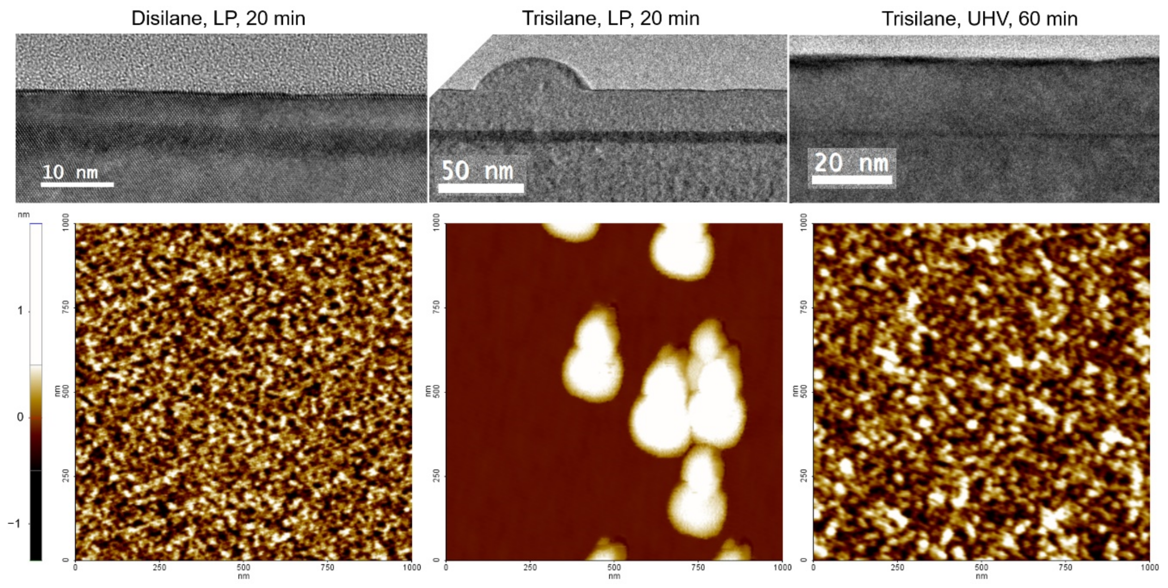
Figure 4 shows the AFM measurements and the root mean square (RMS) surface roughness (Rq) of the Si epilayers grown using disilane and trisilane under UHVCVD conditions at 550 and 600 °C. No particles were found in either case, while the RMS surface roughness of the trisilane samples was higher than that of the disilane samples due to the high growth rate. However, the Si epilayer grown using trisilane at a low pressure demonstrated island formation phenomena, whereas no such phenomena were found for disilane or when using UHVCVD conditions, as shown in
Figure 5.
In the case of silane or dichlorosilane, it is well known that the epitaxial growth behaviors can be simply divided into two regimes: the mass flow limited regime at high temperatures and the reaction rate limited regime at low temperatures. On the other hand, high-order silanes have complicated behaviors depending on the temperature; there are intermediate regions, called plateaus, between the mass flow limited regime and the reaction limited regime [
2,
4]. The growth rate in the intermediate region is relatively independent of the temperature or even increases slightly despite decreasing temperature. This region appears clearly in RPCVD, particularly in H
2 ambient conditions, whereas does not appear in UHVCVD as shown in
Figure 3 (solid line), also reported by Adam et al. [
1]. Hartmann suggested an alternative reaction pathway at the intermediate region, such as Si
2H
6(g) + 2SiH(a) → 2SiH
4(g) + 2Si(s) [
2], and Gouyé suggested similar reactions of trisilane [
4]. However, the intermediate region did not appear in our disilane experiments and appeared very slightly in trisilane and tetrasilane under LPCVD conditions, although the partial pressure of high-order silane of approximately 80 mTorr is similar to the RPCVD studies. This result indicates that the carrier gas plays an important role in the enhancement of growth rates at low temperatures.
Next, disilane- and trisilane-based SiGe epitaxy processes were carried out at 550–650 °C under UHVCVD conditions below 0.1 mTorr. The flow rate of disilane was fixed at 20 sccm, that of trisilane was 5 sccm, and the flow rate of germane varied from 5 to 30 sccm. The growth time was 500 s for all splits. All SiGe epilayers were grown epitaxially, but relaxation occurred in some of the samples because the thickness exceeded the critical thickness. Ge concentrations were measured by HR-XRD, EDS, and SE, as shown in
Table S1. HR-XRD curves are presented in
Figure S3. The results are well-matched except for disilane at 550 °C. The HR-XRD results were used because EDS measures only significantly small regions while HR-XRD is more reproducible than SE. However, when relaxation was observed in TEM images, the Ge concentrations extracted by the HR-XRD curves were considerably smaller than those of EDS and SE. Thus, the Ge concentrations of the highest GeH
4 flow rate at 600 °C were obtained from EDS. Hereafter, the Ge concentration mentioned was obtained from HR-XRD, unless otherwise stated. We note that the Ge concentrations of the SiGe epilayers grown using trisilane are comparable to those grown using disilane even though the flow rate of trisilane is four times lower than that of disilane. This indicates that the Si incorporation of trisilane is four times more effective than that of disilane even though the growth rate of Si epitaxy using trisilane was only two times higher than that of disilane.
The growth rate and Ge concentration versus the Ge flow rate are shown in
Figure 6. The growth rate was proportional to the germane flow rate due to the weaker strength of the Ge–H bond compared to the Si-H bond. When silane is used for SiGe epitaxy at temperatures below 650 °C, the growth rate is highest at a Ge concentration of approximately 10% [
15]. The monotonic increase in the growth rate at a low Ge content is due to the weak strength of the Ge-H bond, as mentioned above. Conversely, the monotonic decrease of the growth rate at high Ge content, particularly at high temperatures, is due to the decrease in the sticking coefficient of silane with increasing Ge content [
15]. However, disilane and trisilane demonstrated a linearly increasing growth rate until the Ge content reached 22% (disilane) or 25% (trisilane) because the sticking coefficient of high-order silane is higher than that of silane. Therefore, high-order silane has the advantage of having a higher growth rate of SiGe epilayers than silane at the same Ge content. The Ge concentration of the SiGe epilayers grown by disilane did not change with increasing temperature, whereas that of trisilane grown at 600 °C was slightly higher than that obtained at 550 °C, as shown in
Figure 6. Gouyé et al. reported the same trend for trisilane in terms of the Ge content in SiGe epitaxy [
4]. However, silane exhibits the opposite characteristics, with the Ge concentration decreasing with increasing temperature [
16]. This phenomenon occurs because the sticking coefficient varies depending on the temperature. Buss et al. reported that the sticking coefficient of disilane is less dependent on the temperature than that of silane [
17]. They fitted the reactive sticking coefficient to the Arrhenius plot for these substances, and the activation energies of silane and disilane at temperatures below 800 °C were calculated to be 55–60 and 35 kJ/mol, respectively. Therefore, the higher-order silane showed a lower dependence of the Ge content on the process temperature.
The RMS surface roughness values of the SiGe epilayers grown by disilane and trisilane at 550 °C were 0.105 and 0.104 nm, respectively, as shown in
Figure 7. These values are below the limitations of the AFM measurements. Conversely, the RMS surface roughness values of the SiGe epilayers grown at 600 °C were 0.386 and 0.736 nm as shown in
Figure 7. These values are slightly higher than those obtained at 550 °C because of the higher obtained growth rate. Similar to Si epitaxy, the surface roughness values of the SiGe epilayers grown under UHVCVD conditions were only affected by the growth rate and not by the precursor species.
SiGe epitaxial growth at 450 °C under UHVCVD conditions was attempted using trisilane; however, epitaxial growth did not occur. Subsequently, high-order silane-based SiGe epitaxy at temperatures below 500 °C was examined under LPCVD conditions. First, various high-order silane and germane ratios were examined. The lack of adequate surface diffusion length is critical for epitaxial growth at low temperatures. If the Ge concentration of a SiGe layer is low, the surface diffusion of an adatom is more difficult to achieve because of the high hydrogen coverage and high strength of the Si-Si and Si-H bonds. Therefore, tetrasilane was first tested because the lowest Ge concentration was expected to be obtained using this compound.
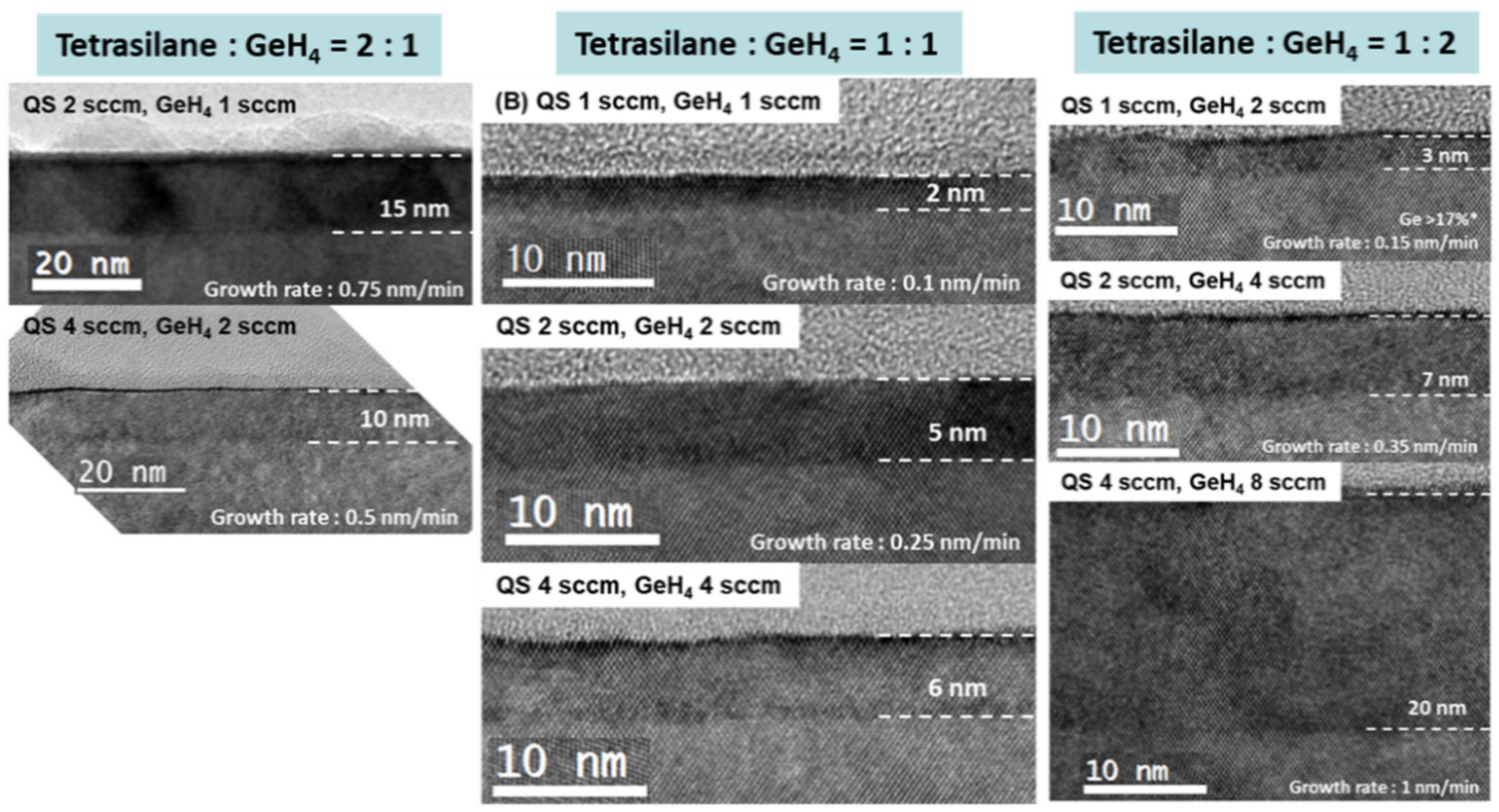
Figure 8 shows the SiGe epilayers grown using tetrasilane at 450 °C. The tetrasilane and germane ratios were 2:1, 1:1, and 1:2. High-quality SiGe layers were obtained at the ratio of 1:2. Consequently, disilane and trisilane were also utilized at the 1:2 ratio. Ge concentrations of the 2:1 ratio samples were lower than those of the other samples; however, most SiGe epilayers grown at 450 °C were too thin to determine the Ge concentration precisely, as shown in
Figure S4.
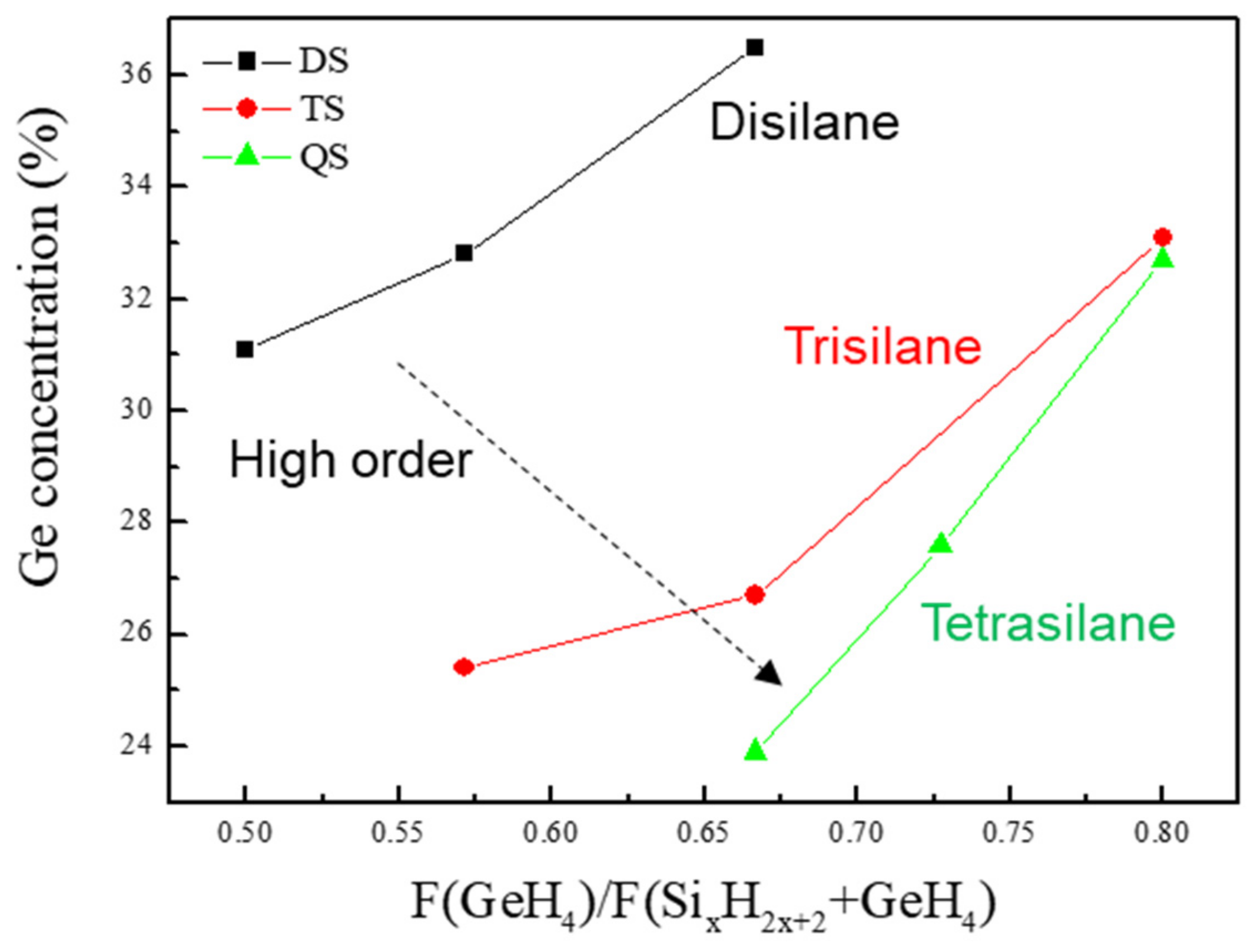
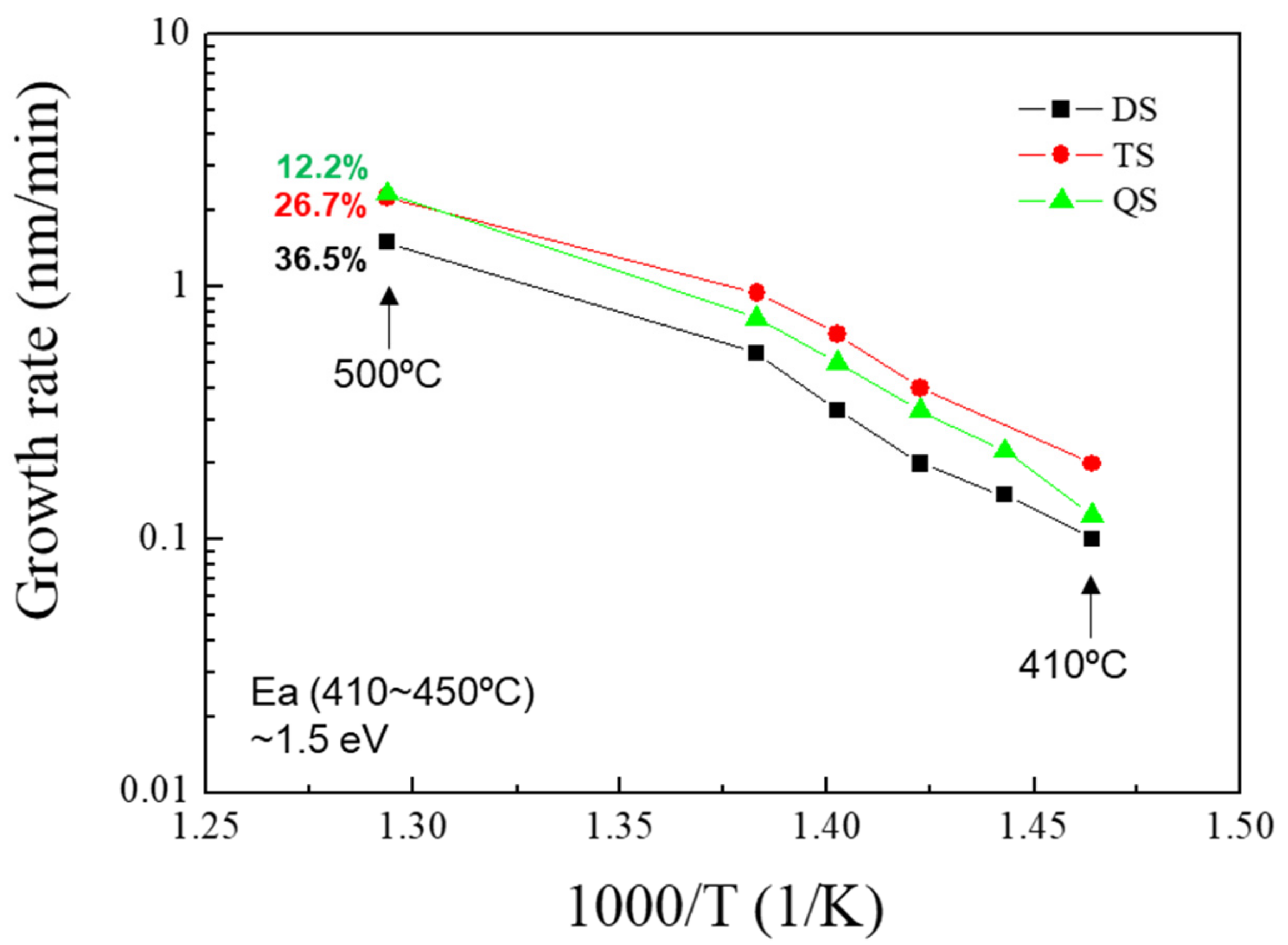
Figure 9 shows the Ge flow rate plotted versus the Ge concentration of the SiGe epilayers grown at 500 °C as the Si precursors. The order of silane was increased while the Ge concentration of the SiGe epilayer was lowered, as expected. The Arrhenius plot for the SiGe epilayers as the Si precursors grown at 410–500 °C is shown in
Figure 10. Trisilane showed the highest growth rate while disilane demonstrated the lowest; however, these rates should not be directly compared due to the different Ge contents. The activation energy was 1.5 eV at 410–450 °C regardless of either the precursor species or the Ge content in the SiGe layer. This is consistent with the values previously reported by Hart et al. for tetrasilane and digermane [
8]. The surface morphology of epitaxial SiGe grown at 500 °C was reported in our previous study [
18]. Similar to Si epitaxy, good morphology was obtained when disilane was used, whereas particle formation was observed when trisilane or tetrasilane was used.


