Review

Variable-Angle Spectroscopic Ellipsometry of Graphene-Based Films

by
Grazia Giuseppina Politano
1,* and
Carlo Versace
1,2
1
Dipartimento di Fisica, Università della Calabria, 87036 Rende, CS, Italy
2
Licryl CNR/Nanotec c/o, Dipartimento di Fisica, Università della Calabria, 87036 Rende, CS, Italy
*
Author to whom correspondence should be addressed.
Coatings 2021, 11(4), 462; https://doi.org/10.3390/coatings11040462
Submission received: 17 March 2021 / Revised: 11 April 2021 / Accepted: 14 April 2021 / Published: 16 April 2021
(This article belongs to the Special Issue Graphene-Based Nanomaterials: Synthesis, Properties, and Applications)

Abstract

:
A review of the authors’ research works on Variable-Angle Spectroscopy (VASE) of graphene-based films is presented. The interaction of graphene oxide (GO) with magnetron-sputtered metals is a promising research area. VASE optical models of GO thin films deposited on magnetron-sputtered titanium (Ti), silver (Ag) and gold (Au) are discussed. Moreover, the optical properties of graphene nanoplatelet (GNPS) films and reduced graphene oxide (RGO) stabilized with Poly(Sodium 4-Styrenesulfonate) (PSS) films, which are less studied graphene-related materials, are shown. Finally, different optical behaviors of chemical vapor deposition (CVD)-grown monolayer, bilayer, and trilayer graphene films on silicon and polyethylene terephthalate (PET) substrates are recapitulated.

1. Introduction

A transparent conductor is a relevant constituent in several photoelectronic appliances. Indium tin oxide (ITO) is principally used for fabricating transparent conductors due to its properties [1]. Nevertheless, ITO has many disadvantages; for instance, it is expensive and it does not find application in flexible devices because of its brittle nature [2]. Consequently, consideration in the semiconductor field has been drawn to graphene [3], which shows broadband light absorption, linear dispersion band structure and an ultrahigh charge-carrier mobility. Graphene-based materials are thus advantageous materials that can be produced in ultrathin sheet form and may be used in several applications [4,5,6,7,8,9,10,11].
Chemical vapor deposition (CVD) is a technique used for high-quality graphene production [12]. The employment of CVD technology in ultradense photonic, optoelectronic, and electronic instruments has been reported [13,14,15].
Graphene oxide (GO) is a graphene-based material that has more oxygen-containing groups and defects in comparison with mechanically exfoliated or CVD-grown graphene. These defects are advantageous to enhance the performance of photodetectors [16]. Additionally, GO thin films show high optical transmittance in the visible region that allows their use as protective coatings and optically transparent electrodes, crucial in solar cells and for optical applications [17].
GO reduction is a method for large scale graphene manufacturing [18]. Reduced graphene oxide (RGO) is achieved using chemical methods [19], which eliminate or diminish the oxygen-containing groups. Additional reduction methods are thermal annealing that should be carried out above 200 °C [20] and “green reducers” (for instance vitamin C) [21].
RGO can be functionalized with Poly(Sodium 4-Styrenesulfonate) (PSS), which is a polyelectrolyte that avoids RGO aggregation. PSS interacts with graphene by means of π-π interactions, is soluble in water and safe to use [22].
Presently graphene nanoplatelets (GNPs) have arisen as a new graphene-based material. GNPs show some of the beneficial properties of single layer graphene [23]. GNPs are composed of mono- to few-layer sheets of sp2 bonded carbon atoms that overlap creating nanometers thick 2D particles [24]. They can be obtained by means of exfoliation of cheap graphite flakes and then through chemical oxidation and graphite oxide nanoplatelets reduction [24].
Graphene-based materials show notable optical properties such as highly transparency in visible spectrum, photo-response up to Terahertz frequency range and tunable infrared optical absorbance [25].
Spectroscopic Ellipsometry (SE) [26] is an highly precise optical method designed for studying the optical properties of materials.
SE has been extensively used to study graphene-based films. The complex refractive index of monolayer graphene has been investigated using SE [25,27,28]. In Ref. [29] the optical constants of graphene were studied by means of a phenomenological Fano model. The optical properties of thick as well as few-layer GO and RGO were studied using SE [30,31].
We present a review of the authors’ research works on Variable-Angle Spectroscopy (VASE) of graphene-based films [32,33,34,35,36,37,38,39].
Despite the availability of literature on SE of graphene-based materials [40], there are not reviews about the optical interaction of GO with magnetron-sputtered metals studied using VASE, which is a promising research area. Moreover, we report about VASE optical model of less studied graphene-based materials such as GNPs and RGO stabilized with PSS films; particular attention to CVD-grown graphene on flexible substrates is given.
The “Results and discussion” part of this review is divided in three main sections. In Section 3.1: “Interaction of graphene oxide with magnetron-sputtered films” the optical properties of GO dip-coated on magnetron-sputtered titanium (Ti), gold (Au) and silver (Ag) thin films were discussed.
In Section 3.2: “Optical properties of graphene-based thin films” the optical properties of GO, thermally reduced graphene oxide, RGO stabilized with PSS and GNPs films were summarized.
Finally, in Section 3.3 “Optical properties of CVD-grown monolayer, bilayer, and trilayer graphene” the optical properties of CVD-grown monolayer graphene samples were reported. In addition, the optical study of CVD-grown bilayer and trilayer graphene samples on silicon and polyethylene terephthalate (PET) substrates was summarized.

2. Materials and Methods

Ellipsometry measures two values ∆ and Ψ.
The two quantities (∆ and ψ ) are measured as a function of incident angle and wavelength and are defined in Equations (1) and (2) [26]:
tan ψ = | R p | | R s |
Δ = δ p δ s
The tangent of the angle Ψ provides thus the ratio of the amplitude attenuation or magnification upon reflection for the p and s polarizations, its value can be from zero to 90°. ∆, instead, provides the difference between the phase shifts experienced upon reflection by the p and s polarizations. The value of ∆ can be between zero and 360°.
The terms p and s denote the incident plane and the perpendicular direction to the incident plane.
The complex quantity ρ , which is the complex ratio of the total reflection coefficients, is defined in Equation (3):
ρ = tan ( Ψ ) e i Δ = R p R s
where Rp and Rs include information on the properties of the materials that are investigated. The use of a capital R implies that the actual material structure can be multilayered and/or multicomponent.
The ellipsometric angles ψ and Δ spectra were obtained using a V-Vase (Woollam Co., Lincoln, NE, USA) ellipsometer (Rotating Analyzer Ellipsometer configuration with AutoRetarder) or a M2000 F (Woollam Co., Lincoln, NE, USA) ellipsometer (Rotating Compensator Ellipsometer).
The optical models were evaluated using WVASE32 application by means of the nonlinear Levenberg-Marquardt algorithm [41]. The minimum value of the Mean Square Error (MSE) [26] is defined in Equation (4):
MSE = 1 2 N M i = 1 N [ ( ( ψ i mod ψ i exp ) σ ψ , i exp ) 2 + ( ( Δ i mod Δ i exp ) σ Δ , i exp ) 2 ]  
where N is the data points number, M is the fitting parameters number, ( Ψ exp , Δ exp )   and ( Ψ mod , Δ mod )   are the experimental and modeled ellipsometric angles, σ ψ and σ Δ are the measured ellipsometric angles standard deviations. The modeled ellipsometric angles ( Ψ mod , Δ mod )   are functions of all fit parameters.
GO and graphene-based dispersions, discussed in this review, were bought from “Sigma Aldrich (St. Louis, MO, USA)” and “Punto Quantico (Roma, Italy)”.
CVD-grown monolayer, bilayer, and trilayer were bought from Graphenea Co. (San Sebastián, Spain). Additional details about the materials and the substrates discussed in this review can be found in Refs. [32,33,34,36,37,38,39].

3. Results and Discussion

3.1. Interaction of Graphene Oxide with Magnetron-Sputtered Films

3.1.1. VASE Study of Electrophoretically Deposited Graphene Oxide and Reduced Graphene Oxide Thin Films

Electrophoretic deposition (EPD) is extensively employed for GO thin films deposition [42,43,44]. The GO platelets are negatively charged because of the plentiful deprotonated carboxylate groups, hence they are electrophoretically drawn to the positive electrode and make a film when a direct current voltage is applied.
The optical study of the GO films electrophoretically deposited on Ti was carried out using VASE, before and after the annealing, and reported in Ref. [39].
The optical models of GO and RGO films are represented respectively by a combination of two and three Lorentz oscillators (Equation (5)):
ε ˜ ( h ν ) = ε 1 + i ε 2 = ε + k = 1 N A k E k 2 E 2 i Γ k E
E is the incident photons energy, ε is the dielectric function real part with E , A k is the contribution of each oscillator k to the system, Γ k is the broadening end E k is the central energy of the k-th oscillator.
Figure 1a,b shows the optical constants dispersion curves in the (300–1000) nm wavelength range.
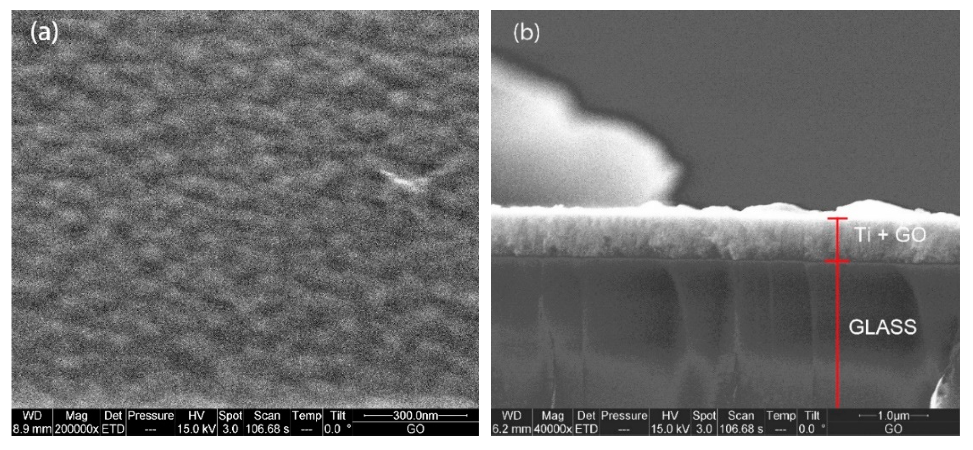
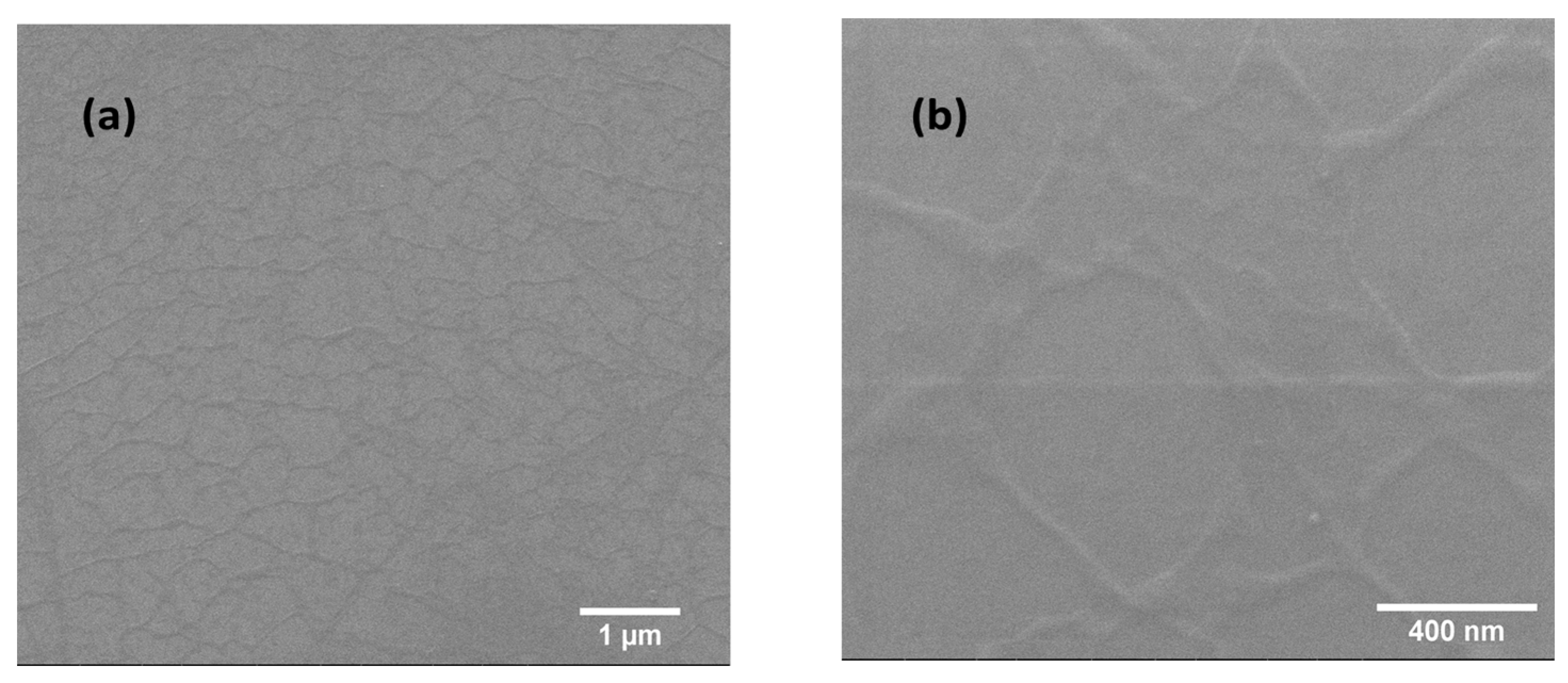
In Figure 2 and Figure 3 Scanning Electron Microscope (SEM) images of GO and RGO samples deposited using EPD technique on Ti are reported.
After GO reduces to RGO, the amount of oxygen declines, a change from sp3 to sp2 hybridization happens and the main peak moves from 5.1 to 4.6 eV [31,45]. It has been shown previously that increased electron-hole (e-h) interactions in RGO implied an increased excitonic effect with a red-shift of the absorption peak of RGO [46,47]. This result is attributable to the Van Hove singularity in the density of states of graphene [48].
In comparison with other research works [31,45,49], using EPD we have obtained higher optical constants.

3.1.2. VASE Investigation of the Optical Properties of Graphene Oxide Dip-Coated on Magnetron-Sputtered Gold Thin Films

Dip-coating [50] was employed for the deposition of GO films on magnetron-sputtered Au thin films [38].
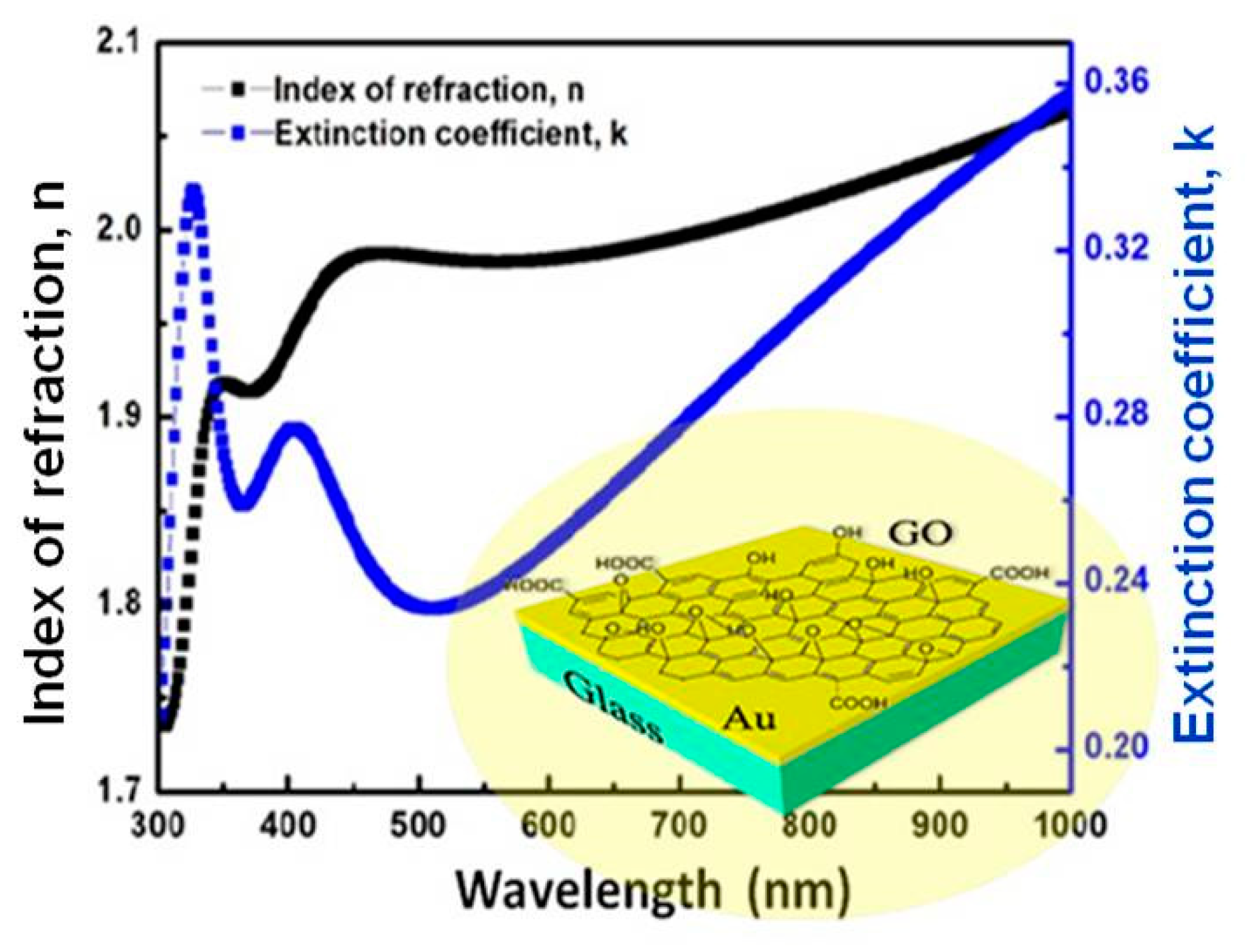
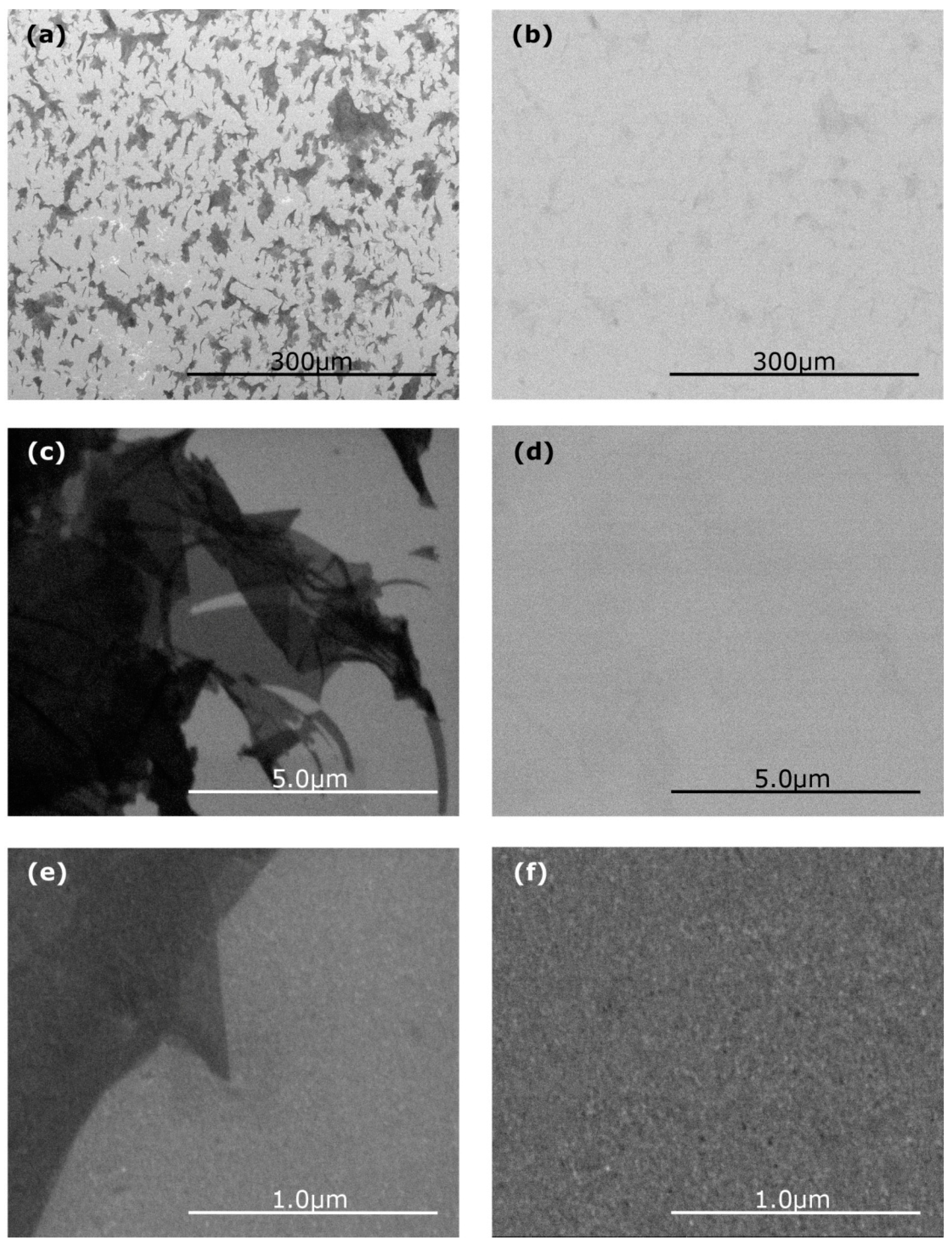
Figure 4 shows the dispersion laws of the GO/Au samples in the (300–1000) nm wavelength range. In Figure 5, SEM images of the GO thin film dip-coated on magnetron-sputtered Au are shown.
The dispersion model of GO/Au samples was described using a combination of three Lorentz oscillators (Equation (5)).
The optical model for GO/Au samples is described by three oscillators at 3.1, 1.8 and 3.8 eV.
GO absorbs mostly in the UV region [1]; the oscillator at 3.8 eV is due to n π * transition of C=O bond [51]. The oscillator at about 1.8 eV denotes different coverage of mixed hydroxyl groups and oxygen atoms [31]. By means of Au magnetron-sputtered thin films as substrates, GO absorbs also in the visible region and the peak of the extinction coefficient k is at ~3.1 eV, which may be described in terms of strong metal-GO interactions.
As reported in Ref. [38], GO/Au thin films could improve GO optical properties, conserving the oxygen amount of GO without the reduction method [52].

3.1.3. VASE Investigation of the Optical Properties of Graphene Oxide on Magnetron-Sputtered Silver Thin Films

The optical characterization was performed on GO deposited by dip-coating on magnetron-sputtered Ag as reported in Ref. [37].
The optical model of GO dip-coated on Ag is described using a combination of three Lorentz oscillators and a Drude-like oscillator (Equation (5)).
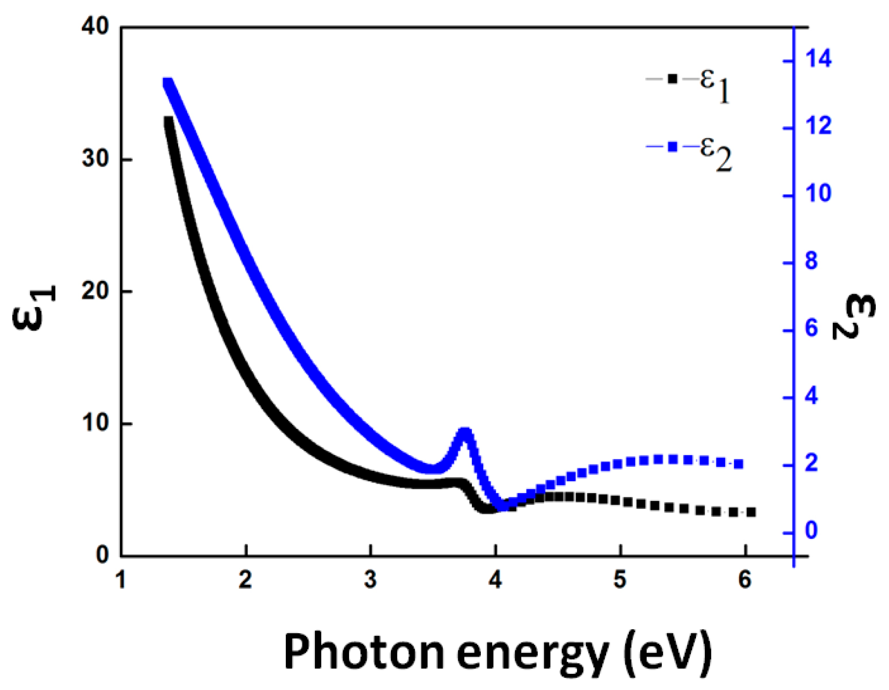
In Figure 6, the optical constants dispersion curves are reported in the (190–900) nm wavelength range.
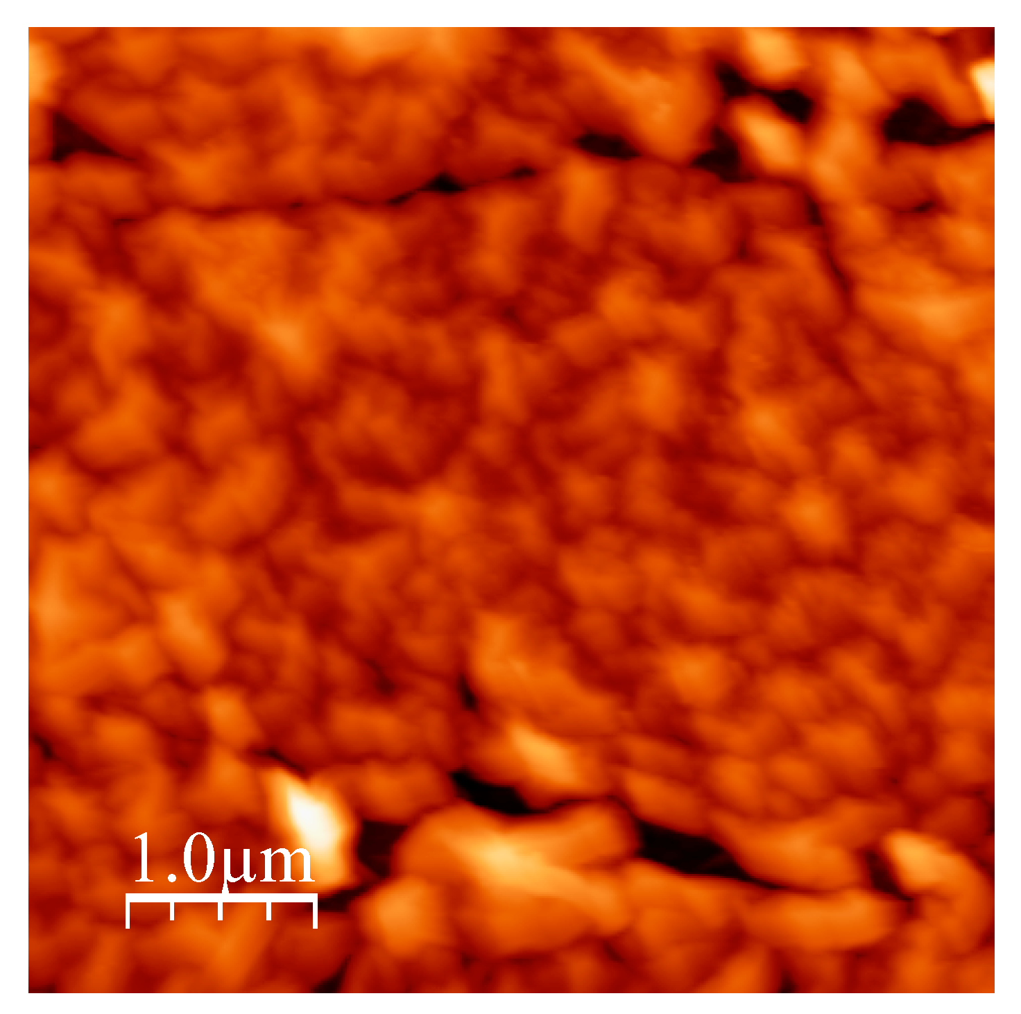
Figure 7 shows a 5 μm × 5 μm an Atomic Force Microscopy (AFM) image of GO thin film dip-coated on magnetron-sputtered Ag.
The optical model in the visible and in the ultraviolet region is represented by three Lorentz oscillators (Equation (5)). The Drude oscillator describes the free-carriers in the near-infrared and, consequently, the conductive properties of GO on magnetron-sputtered Ag. The oscillator at 3.8 eV is attributable to the silver volume plasmon [53], whereas the oscillator at 5.4 eV is due to the π plasmon above ~4 eV in graphene and graphite [54].
Remarkably, these films may be useful for hyperbolic metamaterials, as reported in the Effective medium Theory simulations in our work in Ref. [37].
It is worth noticing that VASE measurements were carried out also for Ag/GO/Au sandwich structures, as reported in Ref. [35].

3.2. Optical Properties of Graphene-Based Thin Films

3.2.1. VASE Characterization of GO and Thermally Reduced RGO Thin Films on Si/SiO2 Substrates

The optical properties of GO and thermally reduced GO (RGO) films were investigated in Ref. [32].
GO and RGO optical properties were obtained using a Lorentz oscillator model (Equation (5)), in accordance with Kramers-Kronig relationships [55].
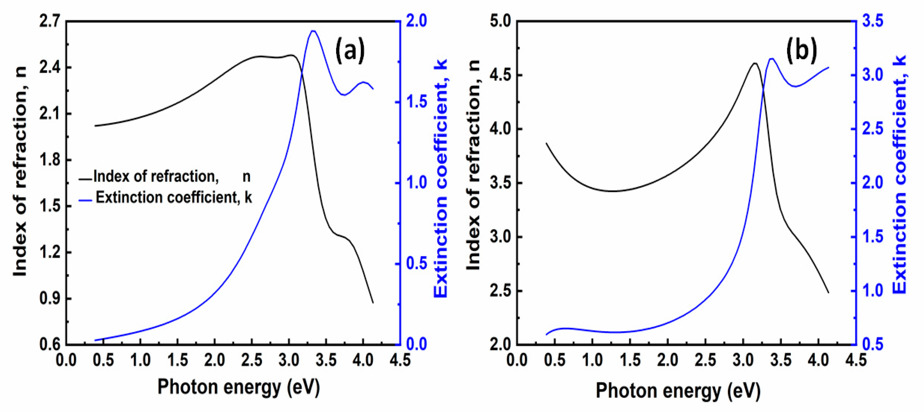
In GO optical model, the oscillator at ~ 2.8 eV represents a coverage of mixed oxygen atoms and hydroxyl groups [31,56]. The oscillator at ~ 3.2 eV denotes a transition that is close to the shoulder of GO absorbance spectrum and near the wavelength of RGO’s blue luminescence [57]. The oscillator at ~ 3.9 eV is attributable to the small shoulder of GO in the absorbance spectrum [57].
In RGO optical model, the oscillator at ~ 2.1 eV represents coverage of mixed oxygen atoms and hydroxyl groups [31]. The oscillator at ~ 3.17 eV could be attributable to the narrow photoluminescence peak of RGO [57]. In Ref. [58] excitonic features noticeable on RGO films between 4 and 4.4 eV are reported. The oscillator at ~ 4 eV is included in that range.
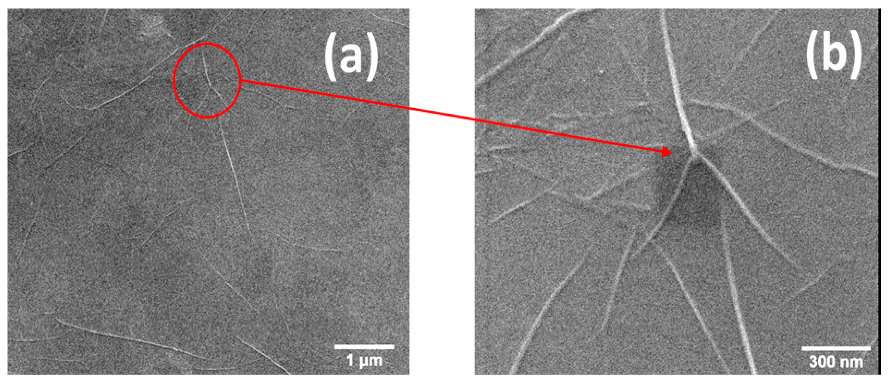
Figure 8a,b show the dispersion laws of GO and RGO films on Si/SiO2 substrates in the (0.38–4.1) eV photon energy range. Figure 9 and Figure 10 show SEM images of GO and RGO films on SiO2/Si.

3.2.2. VASE Characterization of Reduced Graphene Oxide Stabilized with Poly(Sodium 4-Styrenesulfonate)

The optical properties of PSS-functionalized RGO films were investigated in Ref. [32] and were described by a Lorentz model (Equation (5)).
In PSS-RGO optical model, the oscillator at ~ 2.8 eV is attributable to new states that are created by macro sp2 carbon sheet formation throughout the reduction process [59].
Figure 11 shows the dispersion laws of PSS-functionalized RGO films on Si/SiO2 substrates in the (0.38–4.1) eV photon energy range.
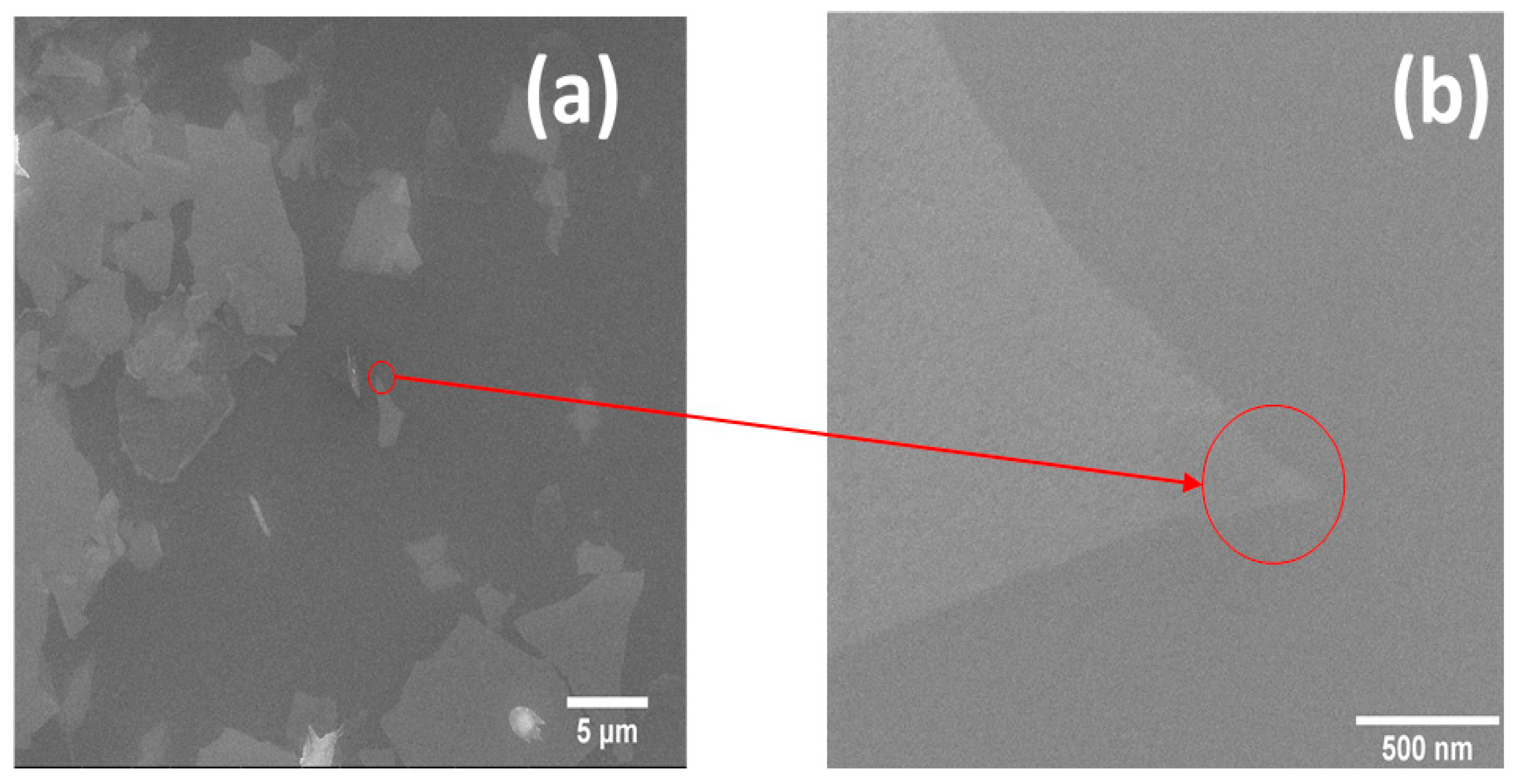
In Figure 12, SEM images of PSS-functionalized RGO films on SiO2/Si substrates are shown.

3.2.3. VASE Study of Graphene Nanoplatelets Thin Films on Si/SiO2 Substrates

The optical study of GNPs films was carried out using VASE in Ref. [34] and the optical model is described using three Gaussian oscillators [60]. Each oscillator has three fit parameters (energetic position, amplitude, and broadening). Equation (6) describes the Gaussian oscillators:
ε 2 , Gauss = A [ exp ( 2 ln 2 ( E ph E c ) B ) 2 exp ( 2 ln 2 ( E ph + E c ) B ) 2 ]
A is the amplitude, B is the broadening, E ph   is the light energy and E c is the oscillator energy [60].
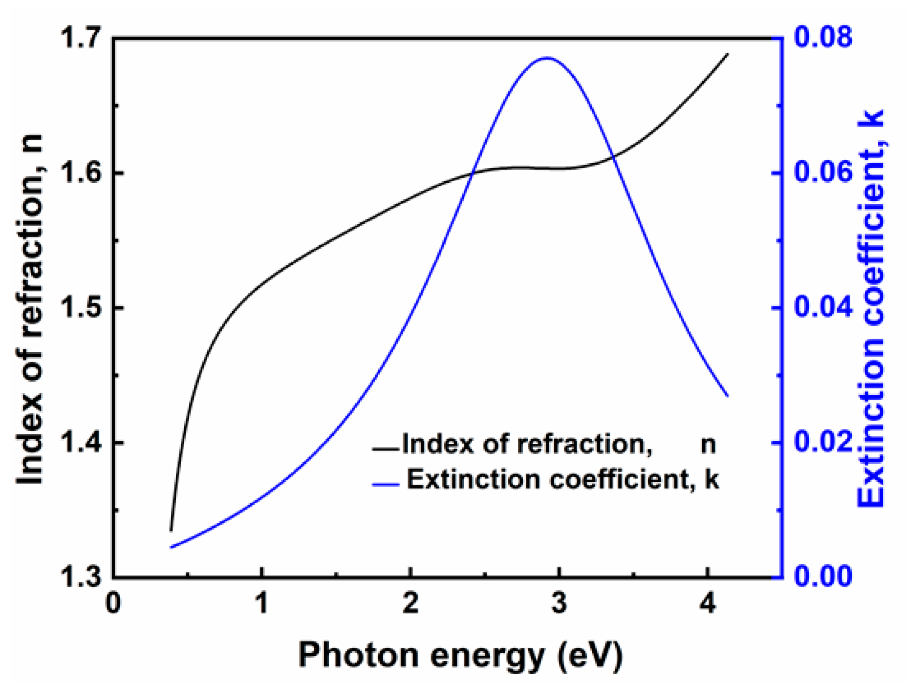
The dispersion laws of GNPs dip-coated on Si/SiO2 substrates are reported in Figure 13 in the (300–1000) nm wavelength range. SEM images of GNP thin film dip-coated on Si/SiO2 substrates are reported in Figure 14.
The oscillator at 3.7 eV agrees with the bulk and surface interlayer state of graphite, whereas the oscillator at 2.7 eV is attributable to defects [61] and the oscillator at ~ 1.5 eV is in accordance with π* band of graphite [61].
In Ref. [62], it was stated that GNPs show an index of refraction n of 1.42 at 482 nm. Therefore, GNPs thin films display lower optical constants than GO [32] and graphene [36].

3.3. Optical Properties of CVD-Grown Monolayer, Bilayer, and Trilayer Graphene

3.3.1. VASE Investigation of CVD-Grown Monolayer Graphene

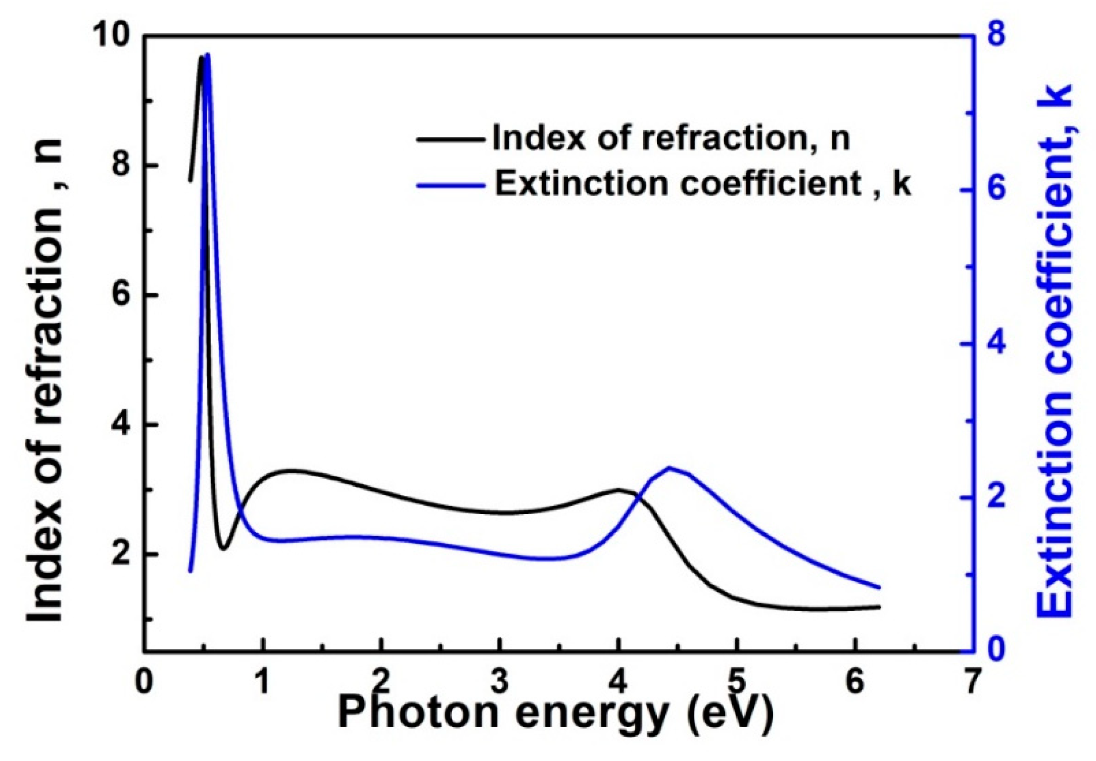
The optical properties of CVD-grown graphene on Si/SiO2 were reported in Ref [36] and were described using four Lorentz oscillators (Equation (5)). The absorption peak at 4.5 eV is attributable to the effects of resonant excitons on the interband transition peak [63]. The oscillator at 2.36 eV is linked to the resonant excitonic effects attributable to the e-h interaction in the π and π * at the M point [63], whereas the oscillator at ∼2.8 eV is due to the hopping amplitude that gives rise to the Dirac nature of low lying excitations [64]. At ~0.5 eV a conducting layer with Drude-like electrons is observed.
Figure 15 shows the estimated dispersion laws of CVD-grown monolayer graphene in the photon energy range between 0.38 and 6.2 eV. Figure 16 shows a 1 μm × 1 μm AFM image of the sample.
The doping concentration, whose extracted value is n 7.8 × 10 13 c m 2 , was obtained from the optical conductivity data.

3.3.2. VASE Characterization of Turbostratic CVD-Grown Bilayer and Trilayer Graphene on Si/SiO2

The VASE study of bilayer and trilayer graphene with random stacking orientation obtained by CVD synthesis on Si/SiO2 is reported in Ref. [33].
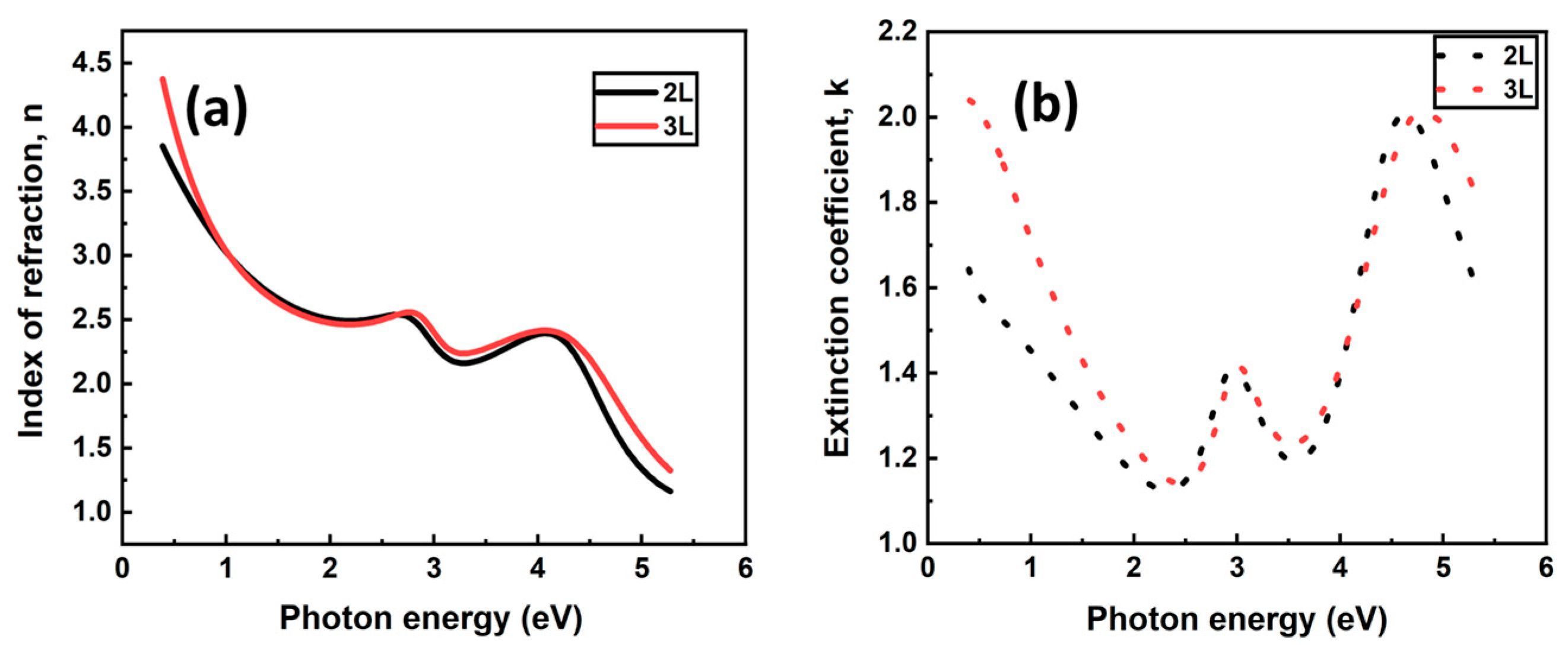
The optical models of bilayer and trilayer graphene on silicon are composed of two Lorentz oscillators (Equation (5)) and a pole.
The oscillator energy at ~ 4.4 eV for CVD-grown bilayer graphene is due to the peak due to the Van Hove singularity in the density of states [65], with a red-shift from 4.6 eV in single layer graphene to 4.4 eV for bilayer graphene [66]. Hence, such peak shift happens also in non-AB stacked graphene samples, as discussed in Ref. [25].
The oscillator energy at ~ 4.56 eV for trilayer graphene is linked to the above-mentioned peak that is visible in the absorbance pattern of trilayer graphene at ~4.6 eV [67].
The extinction coefficient peaks in the optical spectra of bilayer and trilayer graphene on silicon at ~ 3 eV are due to the nearest neighbor term t ≈ 3 eV [65].
In Figure 17a,b, the dispersion laws of CVD-grown bilayer and trilayer graphene samples on silicon in the (0.38–5.2) eV photon energy range are reported.
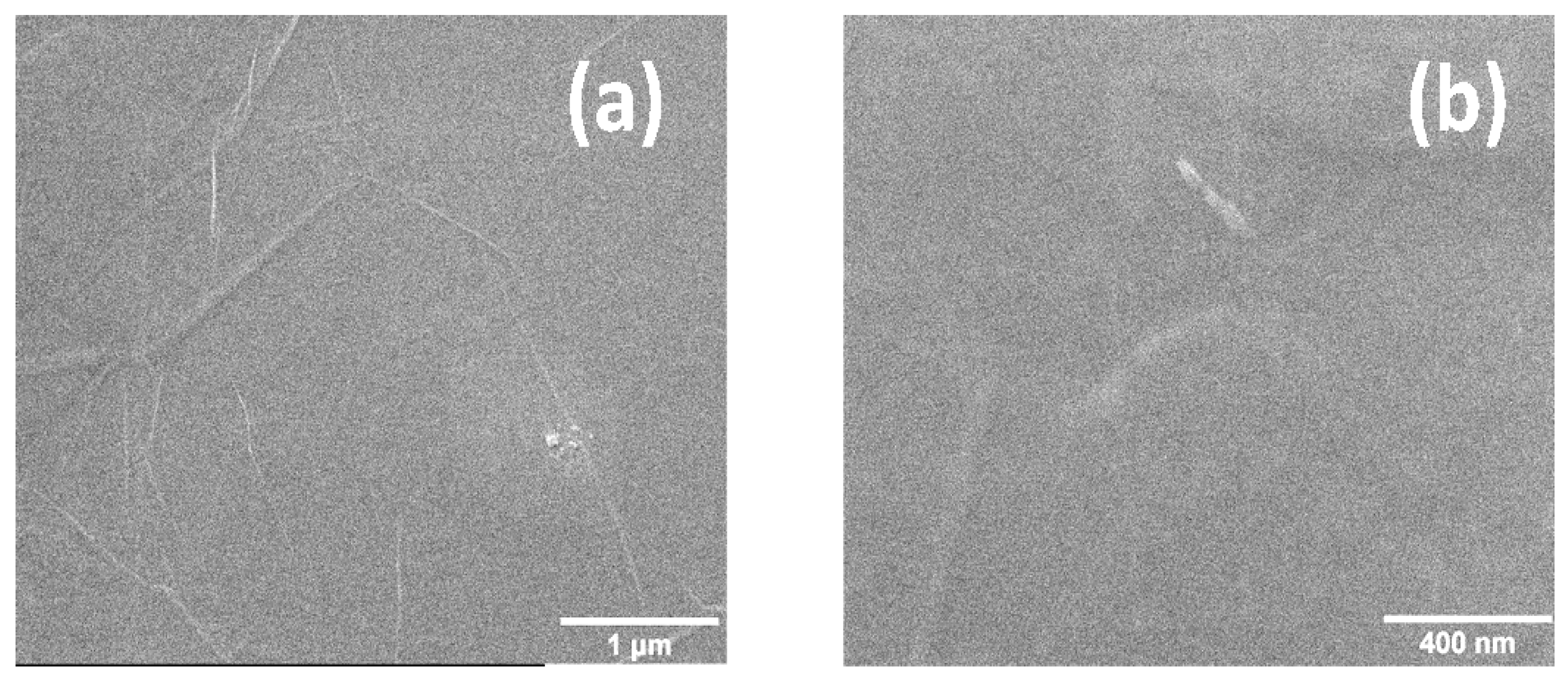
In Figure 18 and Figure 19, SEM images of CVD-grown bilayer and trilayer graphene on SiO2/Si are reported.

3.3.3. VASE Characterization of Turbostratic CVD-Grown Monolayer, Bilayer and Trilayer Graphene on PET

The optical models of monolayer, bilayer, and trilayer graphene samples on PET were represented using two Lorentz oscillators (Equation (5)) and were reported in Ref. [33]. The oscillators at 4.6 eV are due to the Van Hove singularity in the graphene’s density of states. Remarkably, the red-shift of this peak is not reported, while it was visible on bilayer graphene on silicon. Consequently, the red-shift of the absorption peak is dependent on the substrate. Oscillators at ~ 4 eV are attributable to transitions between π and π* in graphite [68].
In Figure 20a,b, the dispersion laws of CVD-grown monolayer graphene, bilayer and trilayer on PET substrates in the (4–5.2) eV photon energy range are reported.

4. Conclusions and Outlook

This article presents a review of the authors’ research works on VASE of graphene-based films.
In the section “Interaction of graphene oxide with magnetron-sputtered films” the optical properties of GO dip-coated on magnetron-sputtered Ti, Au, and Ag thin films are reported.
GO and RGO thin films deposited on Ti substrates were obtained by EPD. The thermal annealing changes the optical properties because some sp3 bonds initially existing in GO were eliminated during this process. In comparison with other investigations, using EPD we obtained higher optical constants.
In addition, the optical properties of GO dip-coated on magnetron-sputtered Au are reported and three Lorentz oscillators were used for the model. Due to the strong interaction Au-GO, GO thin films dip-coated on Au absorbed in the visible region, with a peak of the extinction coefficient k at 3.1 eV. The improved optical properties of GO-Au thin films may be useful in many applications.
The optical properties of GO layers dip-coated on magnetron-sputtered Ag substrates are summarized in the same section. The optical constants were described with a set of Drude-like and Lorentz oscillators. An oscillator at 3.8 eV is attributable to the volume plasmon of silver, whereas another at 5.4 eV is due to the π plasmon above ~4 eV in graphene and graphite. Remarkably, these composite structures of GO on magnetron-sputtered Ag thin films may find use in the field of multilayer hyperbolic metamaterials.
In the section “Optical properties of graphene-based thin films” the optical properties of GO, RGO, and RGO stabilized with PSS on SiO2 substrates are reported. The optical models of GO and RGO films are described using three Lorentz oscillators, while the model of PSS-functionalized RGO films is composed of a Lorentz oscillator and a pole.
In addition, the VASE optical model of GNPs thin films on silicon substrates is discussed. The optical model of GNPs was described with three Gaussian oscillators: the oscillator at 3.7 eV agrees with the surface and bulk interlayer state of graphite, whereas another at 2.7 eV is attributable to defects and the oscillator near 1.5 eV is linked to the π* band of graphite.
In the section “Optical properties of CVD-grown monolayer, bilayer, and trilayer graphene” the broadband optical properties of commercial monolayer CVD-grown monolayer graphene samples are reviewed. The CVD-grown monolayer graphene was modeled with four Lorentz oscillators and the carrier density extracted from optical conductivity data is n 7.8 × 10 13 c m 2 .
In the same section, VASE measurements on random stacked oriented CVD-grown bilayer and trilayer graphene on silicon are recapitulated. Furthermore, VASE optical models of random stacked oriented CVD-grown monolayer, bilayer, and trilayer graphene samples on PET substrates are discussed. An absorption peak red-shift is observed from 4.6 to 4.4 eV on bilayer graphene on silicon, while this peak shift is not detected on PET substrates. An absorption peak at ~3 eV is evident on CVD-grown bilayer and trilayer graphene on silicon samples due to e-h interactions.
It is no doubt that VASE is among the most valuable tools for studying graphene-based films and it is well-suited for many industrial applications.
As in other fields, research on graphene-based applications using VASE has seen dramatic development and it is expanding fast. The advances made in this area are stimulating and hopeful; nevertheless, the challenges are also enormous and should be overcome.
Future investigation on VASE of GO films should mainly focus on a much deeper understanding of the reduction mechanism. In fact, further studies on the controllable oxidation and reduction of GO could improve its use as semiconductor for transistor and photoelectronic devices.
Moreover, there are several ways that graphene-based films can be functionalized for use in different applications. For instance, VASE could be used to study the optical properties of compounds made by combining graphene-based material with other 2D materials. For instance, multilayers made alternating GO and Molybdenum disulfide (MoS2) could be used for metamaterials with application in energy storage.
Another possible application of VASE may be the research on mixing graphene-based materials with matrix polymers, such as polyvinyl alcohol (PVA), to provide an original synthesis route to make graphene-polymers nanocomposites. It would be also interesting studying functional hybrid material composed of CVD-grown graphene on PET substrates and magnetron-sputtered Au and/or Ag for flexible high-performance graphene photodetectors.

Funding

This research received no external funding.

Institutional Review Board Statement

Not applicable.

Informed Consent Statement

Not applicable.

Conflicts of Interest

The authors declare no conflict of interest.

References

  1. Zheng, Q.; Li, Z.; Yang, J.; Kim, J.-K. Graphene oxide-based transparent conductive films. Prog. Mater. Sci. 2014, 64, 200–247. [Google Scholar] [CrossRef]
  2. Bouten, P.C.P.; Slikkerveer, P.J.; Leterrier, Y. Mechanics of ITO on plastic substrates for flexible displays. Flex. Flat Panel Displays 2005, 99–120. [Google Scholar] [CrossRef]
  3. Geim, A.K.N.; Novoselov, K.S. The Rise of Graphene. Nat. Mater. 2007, 6, 183–191. [Google Scholar] [CrossRef] [PubMed]
  4. Manasoglu, G.; Celen, R.; Kanik, M.; Ulcay, Y. An investigation on the thermal and solar properties of graphene-coated polyester fabrics. Coatings 2021, 11, 125. [Google Scholar] [CrossRef]
  5. Abakah, R.R.; Huang, F.; Hu, Q.; Wang, Y.; Jing, L. Comparative study of corrosion properties of different graphene nanoplate/epoxy composite coatings for enhanced surface barrier protection. Coatings 2021, 11, 285. [Google Scholar] [CrossRef]
  6. Dou, B.; Xiao, H.; Lin, X.; Zhang, Y.; Zhao, S.; Duan, S.; Gao, X.; Fang, Z. Investigation of the anti-corrosion properties of fluorinated graphene-modified waterborne epoxy coatings for carbon steel. Coatings 2021, 11, 254. [Google Scholar] [CrossRef]
  7. Baibarac, M.; Daescu, M.; Fejer, S.N. Optical evidence for the assembly of sensors based on reduced graphene oxide and polydiphenylamine for the detection of epidermal growth factor receptor. Coatings 2021, 11, 258. [Google Scholar] [CrossRef]
  8. Imae, I. Reduction of graphene oxide using an environmentally friendly method and its application to energy-related materials. Coatings 2021, 11, 297. [Google Scholar] [CrossRef]
  9. Zhou, Z.-M.; Wang, K.; Wang, Y.-H. High Performance of thermoplastic polyurethane-graphene oxide self-healing composite film. coatings 2021, 11, 128. [Google Scholar] [CrossRef]
  10. Chen, X.; Zhang, Y.; Li, S.; Geng, Y.; Hou, D. Influence of a new type of graphene oxide/silane composite emulsion on the permeability resistance of damaged concrete. Coatings 2021, 11, 208. [Google Scholar] [CrossRef]
  11. Yung, T.-Y.; Lu, Y.-C.; Chen, J.-S.; Cheng, Y.-W.; Liu, T.-Y.; Chen, P.-T. Reinforcement of epoxy resin by additives of amine-functionalized graphene nanosheets. Coatings 2021, 11, 35. [Google Scholar] [CrossRef]
  12. Zhang, Y.; Zhang, L.; Zhou, C. Review of chemical vapor deposition of graphene and related applications. Acc. Chem. Res. 2013, 46, 2329–2339. [Google Scholar] [CrossRef] [PubMed]
  13. Ahmadivand, A.; Gerislioglu, B.; Ramezani, Z. Gated graphene island-enabled tunable charge transfer plasmon terahertz metamodulator. Nanoscale 2019, 11, 8091–8095. [Google Scholar] [CrossRef] [PubMed]
  14. Wang, Z.; Uzlu, B.; Shaygan, M.; Otto, M.; Ribeiro, M.; Marín, E.G.; Iannaccone, G.; Fiori, G.; Elsayed, M.S.; Negra, R.; et al. Flexible one-dimensional metal–insulator–graphene diode. ACS Appl. Electron. Mater. 2019, 1, 945–950. [Google Scholar] [CrossRef] [Green Version]
  15. Kim, H.; Ahn, J.-H. Graphene for flexible and wearable device applications. Carbon N. Y. 2017, 120, 244–257. [Google Scholar] [CrossRef]
  16. Zhu, M.; Li, X.; Guo, Y.; Li, X.; Sun, P.; Zang, X.; Wang, K.; Zhong, M.; Wu, D.; Zhu, H. Vertical junction photodetectors based on reduced graphene oxide/silicon Schottky diodes. Nanoscale 2014, 6, 4909–4914. [Google Scholar] [CrossRef]
  17. Naumov, A.V. Optical properties of graphene oxide. In Graphene Oxide: Fundamentals and Applications; Dimiev, A.M., Eigler, S., Eds.; John Wiley & Sons, Ltd.: Hoboken, NJ, USA, 2016; pp. 147–174. [Google Scholar] [CrossRef]
  18. Pei, S.; Cheng, H.-M. The reduction of graphene oxide. Carbon N. Y. 2012, 50, 3210–3228. [Google Scholar] [CrossRef]
  19. Chua, C.K.; Pumera, M. Chemical reduction of graphene oxide: A synthetic chemistry viewpoint. Chem. Soc. Rev. 2014, 43, 291–312. [Google Scholar] [CrossRef]
  20. Jung, I.; Dikin, D.A.; Piner, R.D.; Ruoff, R.S. Tunable electrical conductivity of individual graphene oxide sheets reduced at “low” temperatures. Nano Lett. 2008, 8, 4283–4287. [Google Scholar] [CrossRef]
  21. MAunkor, T.H.; Mahbubul, I.M.; Saidur, R.; Metselaar, H.S.C. The green reduction of graphene oxide. RSC Adv. 2016, 6, 27807–27828. [Google Scholar] [CrossRef]
  22. Yan, W.; Yu, W.-J.; Wang, L.; Zhang, D.; Ge, X.-Q.; Hang, J.-Z.; Deng, W.; Shi, L.-Y. Preparation of partially reduced graphene oxide nanosheets/poly(sodium 4-styrenesulfonate) composite with high capacitance. Electrochim. Acta 2014, 147, 257–264. [Google Scholar] [CrossRef]
  23. Moosa, A.A.; Sa, A.R.; Ibrahim, M. Mechanical and electrical properties of graphene nanoplates and carbon-nanotubes hybrid epoxy. Nanocomposites 2016, 6, 157–165. [Google Scholar] [CrossRef]
  24. Laurenzi, S.; Santonicola, M.G. 7—Impact Response of Advanced Composite Structures Reinforced by Carbon Nanoparticles; Lopresto, V., Langella, A., Abrate, S., Eds.; Woodhead Publishing: Sawston, UK, 2017; pp. 217–235. [Google Scholar] [CrossRef]
  25. Li, W.; Cheng, G.; Liang, Y.; Tian, B.; Liang, X.; Peng, L.; Walker, A.R.H.; Gundlach, D.J.; Nguyen, N.V. Broadband optical properties of graphene by spectroscopic ellipsometry. Carbon N. Y. 2016, 99, 348–353. [Google Scholar] [CrossRef] [Green Version]
  26. Tompkins, H.; Irene, E.A. Handbook of Ellipsometry; William Andrew: Norwich, NY, USA, 2005. [Google Scholar]
  27. Weber, J.W.; Calado, V.E.; van de Sanden, M.C.M. Optical constants of graphene measured by spectroscopic ellipsometry. Appl. Phys. Lett. 2010, 97, 91904. [Google Scholar] [CrossRef]
  28. Nelson, F.J.; Kamineni, V.K.; Zhang, T.; Comfort, E.S.; Lee, J.U.; Diebold, A.C. Optical properties of large-area polycrystalline chemical vapor deposited graphene by spectroscopic ellipsometry. Appl. Phys. Lett. 2010, 97, 253110. [Google Scholar] [CrossRef]
  29. Matković, A.; Beltaos, A.; Milićević, M.; Ralević, U.; Vasić, B.; Jovanović, D.; Gajić, R. Spectroscopic imaging ellipsometry and Fano resonance modeling of graphene. J. Appl. Phys. 2012, 112, 123523. [Google Scholar] [CrossRef]
  30. Schöche, S.; Hong, N.; Khorasaninejad, M.; Ambrosio, A.; Orabona, E.; Maddalena, P.; Capasso, F. Optical properties of graphene oxide and reduced graphene oxide determined by spectroscopic ellipsometry. Appl. Surf. Sci. 2017, 421, 778–782. [Google Scholar] [CrossRef]
  31. Shen, Y.; Zhou, P.; Sun, Q.Q.; Wan, L.; Li, J.; Chen, L.Y.; Zhang, D.W.; Wang, X.B. Optical investigation of reduced graphene oxide by spectroscopic ellipsometry and the band-gap tuning. Appl. Phys. Lett. 2011, 99, 141911. [Google Scholar] [CrossRef]
  32. Politano, G.; Vena, C.; Desiderio, G.; Versace, C. Variable angle spectroscopic ellipsometry characterization of reduced graphene oxide stabilized with poly(sodium 4-styrenesulfonate). Coatings 2020, 743. [Google Scholar] [CrossRef]
  33. Politano, G.G.; Vena, C.; Desiderio, G.; Versace, C. Variable angle spectroscopic ellipsometry characterization of turbostratic CVD-grown bilayer and trilayer graphene. Opt. Mater. 2020, 107, 110165. [Google Scholar] [CrossRef]
  34. Politano, G.G.; Nucera, A.; Castriota, M.; Desiderio, G.; Vena, C.; Versace, C. Spectroscopic and morphological study of graphene nanoplatelets thin films on Si/SiO2 substrates. Mater. Res. Express. 2019, 6, 106432. [Google Scholar] [CrossRef]
  35. Politano, G.G.; Cazzanelli, E.; Versace, C.; Castriota, M.; Desiderio, G.; Davoli, M.; Vena, C.; Bartolino, R. Micro-Raman investigation of Ag/graphene oxide/Au sandwich structure. Mater. Res. Express. 2019, 6, 075605. [Google Scholar] [CrossRef]
  36. Castriota, M.; Politano, G.G.; Vena, C.; de Santo, M.P.; Desiderio, G.; Davoli, M.; Cazzanelli, E.; Versace, C. Variable Angle Spectroscopic Ellipsometry investigation of CVD-grown monolayer graphene. Appl. Surf. Sci. 2019, 467–468. [Google Scholar] [CrossRef]
  37. Politano, G.G.; Cazzanelli, E.; Versace, C.; Vena, C.; de Santo, M.P.; Castriota, M.; Ciuchi, F.; Bartolino, R. Graphene oxide on magnetron sputtered silver thin films for SERS and metamaterial applications. Appl. Surf. Sci. 2018, 427, 927–933. [Google Scholar] [CrossRef]
  38. Politano, G.G.; Vena, C.; Desiderio, G.; Versace, C. Spectroscopic ellipsometry investigation of the optical properties of graphene oxide dip-coated on magnetron sputtered gold thin films. J. Appl. Phys. 2018, 123, 055303. [Google Scholar] [CrossRef]
  39. Politano, G.G.; Versace, C.; Vena, C.; Castriota, M.; Ciuchi, F.; Fasanella, A.; Desiderio, G.; Cazzanelli, E. Physical investigation of electrophoretically deposited graphene oxide and reduced graphene oxide thin films. J. Appl. Phys. 2016, 120, 195307. [Google Scholar] [CrossRef]
  40. Losurdo, M.; Giangregorio, M.M.; Bianco, G.V.; Capezzuto, P.; Bruno, G. How spectroscopic ellipsometry can aid graphene technology? Thin Solid Films 2014, 571, 389–394. [Google Scholar] [CrossRef]
  41. Moré, J.J. The Levenberg-Marquardt algorithm: Implementation and theory. In Proceedings of the Biennial Conference, Dundee, UK, 28 June–1 July 1977; pp. 105–116. [Google Scholar] [CrossRef] [Green Version]
  42. Lee, V.; Whittaker, L.; Jaye, C.; Baroudi, K.M.; Fischer, D.A.; Banerjee, S. Large-area chemically modified graphene films: Electrophoretic deposition and characterization by soft x-ray absorption spectroscopy. Chem. Mater. 2009, 21, 3905–3916. [Google Scholar] [CrossRef]
  43. An, S.J.; Zhu, Y.; Lee, S.H.; Stoller, M.D.; Emilsson, T.; Park, S.; Velamakanni, A.; An, J.; Ruoff, R.S. Thin film fabrication and simultaneous anodic reduction of deposited graphene oxide platelets by electrophoretic deposition. J. Phys. Chem. Lett. 2010, 1, 1259–1263. [Google Scholar] [CrossRef]
  44. Chavez-Valdez, A.; Shaffer, M.S.P.; Boccaccini, A.R. Applications of graphene electrophoretic deposition. A review. J. Phys. Chem. B 2013, 117, 1502–1515. [Google Scholar] [CrossRef]
  45. Shen, Y.; Yang, S.; Zhou, P.; Sun, Q.; Wang, P.; Wan, L.; Li, J.; Chen, L.; Wang, X.; Ding, S.; et al. Evolution of the band-gap and optical properties of graphene oxide with controllable reduction level. Carbon N. Y. 2013, 62, 157–164. [Google Scholar] [CrossRef]
  46. Kravets, V.G.; Grigorenko, A.N.; Nair, R.R.; Blake, P.; Anissimova, S.; Novoselov, K.S.; Geim, A.K. Spectroscopic ellipsometry of graphene and an exciton-shifted van Hove peak in absorption. Phys. Rev. B 2010, 81, 155413. [Google Scholar] [CrossRef] [Green Version]
  47. Johari, P.; Shenoy, V.B. Modulating optical properties of graphene oxide: Role of prominent functional groups. ACS Nano 2011, 5, 7640–7647. [Google Scholar] [CrossRef] [PubMed]
  48. Chae, D.-H.; Utikal, T.; Weisenburger, S.; Giessen, H.; Klitzing, K.V.; Lippitz, M.; Smet, J. Excitonic fano resonance in free-standing graphene. Nano Lett. 2011, 11, 1379–1382. [Google Scholar] [CrossRef] [Green Version]
  49. Stebunov, Y.V.; Aftenieva, O.A.; Arsenin, A.V.; Volkov, V.S. Highly sensitive and selective sensor chips with graphene-oxide linking layer. ACS Appl. Mater. Interfaces 2015, 7, 21727–21734. [Google Scholar] [CrossRef] [PubMed]
  50. Scriven, L.E. Physics and applications of dip coating and spin coating. MRS Proc. 1988, 121, 717. [Google Scholar] [CrossRef]
  51. Luo, Z.; Lu, Y.; Somers, L.A.; Johnson, A.T.C. High yield preparation of macroscopic graphene oxide membranes. J. Am. Chem. Soc. 2009, 131, 898–899. [Google Scholar] [CrossRef] [PubMed]
  52. Kumar, P.V.; Bardhan, N.M.; Tongay, S.; Wu, J.; Belcher, A.M.; Grossman, J.C. Scalable enhancement of graphene oxide properties by thermally driven phase transformation. Nat. Chem. 2014, 6, 151–158. [Google Scholar] [CrossRef]
  53. Zacharias, P.; Kliewer, K.L. Dispersion relation for the 3.8 eV volume plasmon of silver. Solid State Commun. 1976, 18, 23–26. [Google Scholar] [CrossRef]
  54. Liou, S.C.; Shie, C.-S.; Chen, C.H.; Breitwieser, R.; Pai, W.W.; Guo, G.Y.; Chu, M.-W. π-plasmon dispersion in free-standing graphene by momentum-resolved electron energy-loss spectroscopy. Phys. Rev. B 2015, 91, 45418. [Google Scholar] [CrossRef]
  55. Kubo, R.; Ichimura, M. Kramers-Kronig relations and sum rules. J. Math. Phys. 1972, 13, 1454–1461. [Google Scholar] [CrossRef]
  56. Boukhvalov, D.W.; Katsnelson, M.I. Modeling of graphite oxide. J. Am. Chem. Soc. 2008, 130, 10697–10701. [Google Scholar] [CrossRef] [Green Version]
  57. Bansal, T.; Mohite, A.D.; Shah, H.M.; Galande, C.; Srivastava, A.; Jasinski, J.B.; Ajayan, P.M.; Alphenaar, B.W. New insights into the density of states of graphene oxide using capacitive photocurrent spectroscopy. Carbon N. Y. 2012, 50, 808–814. [Google Scholar] [CrossRef]
  58. Eda, G.; Lin, Y.-Y.; Mattevi, C.; Yamaguchi, H.; Chen, H.-A.; Chen, I.-S.; Chen, C.-W.; Chhowalla, M. Blue photoluminescence from chemically derived graphene oxide. Adv. Mater. 2010, 22, 505–509. [Google Scholar] [CrossRef]
  59. Liang, H.F.; Smith, C.T.G.; Mills, C.A.; Silva, S.R.P. The band structure of graphene oxide examined using photoluminescence spectroscopy. J. Mater. Chem. C 2015, 3, 12484–12491. [Google Scholar] [CrossRef] [Green Version]
  60. J. A. Woollam Co. WVASE Manual “Guide to Using WVASE32”; J. A. Woollam Co.: Lincoln, NE, USA, 2010. [Google Scholar]
  61. Tosatti, E.; Fuchs, H. Unoccupied electronic states of a graphite surface as observed by local tunnelling spectroscopy. EPL 1987, 3, 745. [Google Scholar]
  62. Kumar, D.; Singh, K.; Verma, V.; Bhatti, H.S. Microwave assisted synthesis and characterization of graphene nanoplatelets. Appl. Nanosci. 2016, 6, 97–103. [Google Scholar] [CrossRef] [Green Version]
  63. Yang, L.; Deslippe, J.; Park, C.-H.; Cohen, M.L.; Louie, S.G. Excitonic effects on the optical response of graphene and bilayer graphene. Phys. Rev. Lett. 2009, 103, 186802. [Google Scholar] [CrossRef] [PubMed]
  64. Hadipour, H.; Jafari, S. The importance of electron correlation in graphene and hydrogenated graphene. Eur. Phys. J. B 2015. [Google Scholar] [CrossRef]
  65. Neto, A.H.C.; Guinea, F.; Peres, N.M.R.; Novoselov, K.S.; Geim, A.K. The electronic properties of graphene. Rev. Mod. Phys. 2009, 81, 109–162. [Google Scholar] [CrossRef] [Green Version]
  66. Chang, Y.-C.; Liu, C.-H.; Liu, C.-H.; Zhong, Z.; Norris, T.B. Extracting the complex optical conductivity of mono- and bilayer graphene by ellipsometry. Appl. Phys. Lett. 2014, 104, 261909. [Google Scholar] [CrossRef] [Green Version]
  67. Ke, F.; Chen, Y.; Yin, K.; Yan, J.; Zhang, H.; Liu, Z.; Tse, J.S.; Wu, J.; Mao, H.-K.; Chen, B. Large bandgap of pressurized trilayer graphene. Proc. Natl. Acad. Sci. USA 2019, 116, 9186–9190. [Google Scholar] [CrossRef] [PubMed] [Green Version]
  68. Liu, J.-M.; Lin, I.-T. Graphene Photonics; Cambridge University Press: Cambridge, UK, 2018. [Google Scholar]
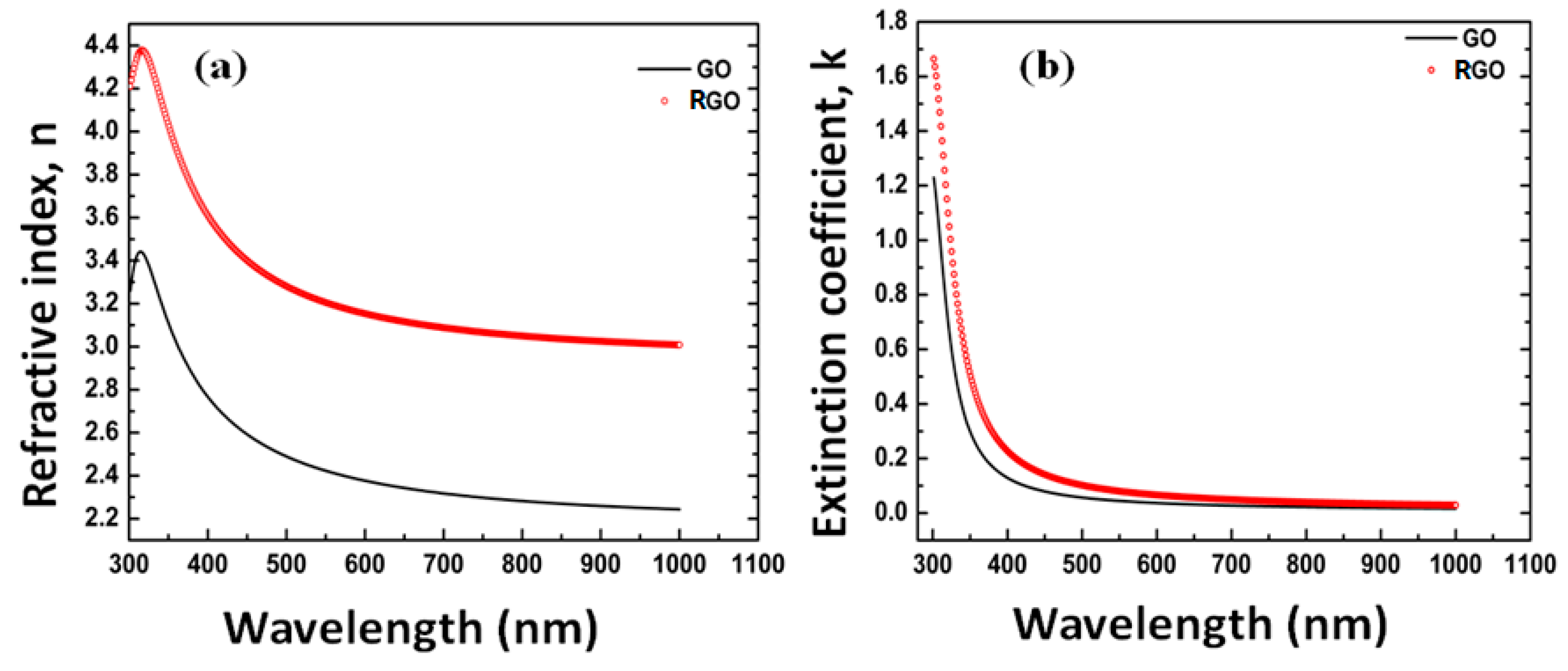
Figure 1. Estimated index of refraction (a) and extinction coefficient (b) of GO (black lines) and RGO (red lines) samples. Reprinted from Ref. [39] with permission from AIP Publishing. Copyright 2016 AIP Publishing.
Coatings 11 00462 g001
Figure 2. (a) Top view of GO on magnetron-sputtered Ti/glass and (b) cross section of the same sample. Reprinted from Ref. [39] with permission from AIP Publishing. Copyright 2016 AIP Publishing.
Coatings 11 00462 g002
Figure 3. (a) Top view of RGO/Ti bilayer on glass substrate and (b) cross section of the same sample. Reprinted from Ref. [39] with permission from AIP Publishing. Copyright 2016 AIP Publishing.
Coatings 11 00462 g003
Figure 4. Estimated index of refraction (black line) and extinction coefficient (blue line) of GO/Au thin film by VASE characterization with a sketch of the structure in the inset. Reprinted from Ref. [38] with permission from AIP Publishing. Copyright 2018 AIP Publishing.
Coatings 11 00462 g004
Figure 5. SEM images of GO thin film dip-coated on magnetron-sputtered Au (a,b), and related magnifications (cf). (a,c,e) were obtained using secondary electron detector, whereas (b,d,f) using backscattered electron detector. Reprinted from Ref. [38] with permission from AIP Publishing. Copyright 2018 AIP Publishing.
Coatings 11 00462 g005
Figure 6. Estimated real (black line) and imaginary (blue line) part of the dielectric constant of GO dip-coated on magnetron-sputtered Ag substrate by VASE characterization. Reprinted from Ref. [37] with permission from Elsevier. Copyright 2018 Elsevier.
Coatings 11 00462 g006
Figure 7. AFM image of GO dip-coated on magnetron-sputtered Ag. Reprinted from Ref. [37] with permission from Elsevier. Copyright 2018 Elsevier.
Coatings 11 00462 g007
Figure 8. Estimated index of refraction (black lines) and extinction coefficient (blue lines) of GO (a) and RGO (b) films on silicon substrates by VASE characterization. Reprinted from Ref. [32].
Coatings 11 00462 g008
Figure 9. SEM image of GO films on silicon substrates (a) and its magnification (b). Reprinted from Ref. [32].
Coatings 11 00462 g009
Figure 10. SEM image of RGO films on silicon substrates (a) and its magnification (b). Reprinted from Ref. [32].
Coatings 11 00462 g010
Figure 11. Estimated index of refraction (black line) and extinction coefficient (blue line) of RGO stabilized with PSS on silicon substrates by VASE characterization. Reprinted from Ref. [32].
Coatings 11 00462 g011
Figure 12. SEM image of RGO films stabilized with PSS on silicon substrates (a) and its magnification (b). Reprinted from Ref. [32].
Coatings 11 00462 g012
Figure 13. Estimated index of refraction (black line) and extinction coefficient (blue line) of GNPs thin films on Si/SiO2 substrates. Reprinted from Ref. [34] with permission from IOP Publishing. Copyright 2019 IOP Publishing.
Coatings 11 00462 g013
Figure 14. SEM image of GNPs dip-coated on Si/SiO2 substrates (a) and its magnification (b). Reprinted from Ref. [34] with permission from IOP Publishing. Copyright 2019 IOP Publishing.
Coatings 11 00462 g014
Figure 15. Estimated index of refraction (black line) and extinction coefficient (blue line) of monolayer graphene by VASE characterization. Reprinted from Ref. [36] with permission from Elsevier. Copyright 2019 Elsevier.
Coatings 11 00462 g015
Figure 16. AFM image of a CVD-grown monolayer graphene. Reprinted from Ref. [36] with permission from Elsevier. Copyright Elsevier.
Coatings 11 00462 g016
Figure 17. Estimated index of refraction (a) and extinction coefficient (b) of CVD-grown bilayer (black lines) and trilayer (red lines) graphene samples on silicon by VASE characterization. Reprinted from Ref. [33] with permission from Elsevier. Copyright 2020 Elsevier.
Coatings 11 00462 g017
Figure 18. SEM image of CVD-grown bilayer graphene transferred to SiO2/Si substrate (a) and related magnification (b). Reprinted from Supplementary material of Ref. [33] with permission from Elsevier. Copyright 2020 Elsevier.
Coatings 11 00462 g018
Figure 19. SEM image of CVD-grown trilayer graphene transferred to SiO2/Si substrate (a) and related magnification (b). Reprinted from Supplementary material of Ref. [33] with permission from Elsevier. Copyright 2020 Elsevier.
Coatings 11 00462 g019
Figure 20. Estimated index of refraction (a) and extinction coefficient (b) of CVD-grown monolayer (blue lines), bilayer (black lines) and trilayer graphene (red lines) on PET substrates by VASE characterization. Reprinted from Ref. [33] with permission from Elsevier. Copyright 2020 Elsevier.
Coatings 11 00462 g020
Publisher’s Note: MDPI stays neutral with regard to jurisdictional claims in published maps and institutional affiliations.