Article

Te-Embedded Nanocrystalline PbTe Thick Films: Structure and Thermoelectric Properties Relationship

1
Department of Chemical and Environmental Engineering, University of California-Riverside, Riverside, 900 University Ave, Riverside, CA 92521, USA
2
Department of Materials Science and Engineering, Gachon University, 1342 Seongnamdaero, Sujeong-gu, Seongnam-si 13120, Gyeonggi-do, Korea
3
Electrochemistry Department, Korea Institute of Materials Science, Changwon 51508, Gyeongsangnam-do, Korea
4
Materials Science and Chemical Engineering Center, Institute for Advanced Engineering, Yongin-si 17180, Gyeonggi-do, Korea
*
Authors to whom correspondence should be addressed.
Coatings 2021, 11(3), 356; https://doi.org/10.3390/coatings11030356
Submission received: 26 January 2021 / Revised: 27 February 2021 / Accepted: 9 March 2021 / Published: 21 March 2021
(This article belongs to the Special Issue Thin Films for Electronic Devices)

Abstract

:
The Te-embedded PbTe nanocrystallline thick films (i.e., 50 µm) were electrodeposited, where the fraction and average grain size of PbTe and Te phases were tuned by adjusting the applied potential followed by post thermal treatment. The crystal grain boundary and Te nano-inclusion in the films played critical roles in their thermoelectric properties. The Te-embedded PbTe thick film with the average grain size of around 100 nm showed lower energy barrier height (EB = 0.023 eV) than thick films with the average grain size of a few tens of nm (EB = 0.11). Although decrease in the energy barrier reduced the Seebeck coefficient, however, it enhanced the electrical conductivity, which resulted in an increase in power factor (PF). The highest power factor was 183 μw K−2 cm−1, achieved at the energy barrier of 0.023 eV.

Graphical Abstract

1. Introduction

Heat is the natural by-product of the energy conversion processes. Of the ~4 × 10²⁰ J of energy the USA consumes every year, greater than 60% is wasted in the form of heat [1,2,3]. Thus, waste heat recovery is a crucial step to improve the energy conversion and utilization efficiency. Thermoelectric (TE) materials, which can directly convert waste heat into energy, have been extensively researched for this purpose. The efficiency of a thermoelectric device can be presented by the thermoelectric-figure-of-merit called ZT = S2σT/κ, where S, σ, T, and κ are the Seebeck coefficient, electrical conductivity, temperature, and thermal conductivity, respectively. Two different approaches have been utilized to enhance the ZT of thermoelectric materials, which include the finding of proper thermoelectric materials with suitable carrier concentration values, n, since three interdependent thermoelectric parameters (S, σ, and κ) are functional to the carrier concentration [4]. In addition, nanoengineering of thermoelectric materials (e.g., dimension, superlattices, and second phase-inclusion) has been highlighted as the way to decouple the thermoelectric parameters [5,6,7,8,9,10,11,12,13].
Thermal management of miniaturized electronic components led to need of solid-state micro-coolers and generators. Therefore, fabrication of micro-thermoelectric devices, which typically are based on thin- and thick-films, has drawn a significant amount of attention lately [14]. Especially, the film-based thermoelectric devices have been shown to have many advantages over conventional bulk thermoelectric modules because of their compact size and flexibility. In addition, a micro-thermoelectric device is able to operate under smaller temperature gradients with fast response time, which allow the handling of a wider range of thermal and power management microelectronic systems [14,15,16,17,18]. The electrodeposition has a low operating and facility cost and high deposition rate, which is suitable for commercial application. Additionally, the electrodeposition is able to have selective deposition, which allows easy patterning for small sized-features as well as reduction of waste materials [19]. Various types of micro-thermoelectric devices mostly consisted of Bi2Te3 alloys (n-type) and Sb2Te3 alloys (p-type) were fabricated using the electrodeposition technique [20]. However, approaches to enhance the thermoelectric efficiency were limited to changes of device configuration and heat flow direction, therefore, it is important to combine nano-engineering to manipulate the charge transfer mechanism to further enhance the thermoelectric efficiency.
Using the electrodeposition process, precise control over the chemical composition and microstructure (e.g., crystallinity, crystal structure, preferred orientation, and the attainment of nano-inclusions and/or intermetallic phases) yields improved thermoelectric properties. Additionally, for lead telluride, nanoengineering can also introduce phonon scattering and quantum confinement effect to optimize the thermoelectric properties [9,10,11]. Lead telluride (PbTe) is a known candidate for mid-range temperature thermoelectrics showing the great performance at temperature range between 400 and 600 K. The electrodeposition method has been also applied for a synthesis of the PbTe thin films in acidic media [21,22,23,24,25,26,27,28]. However, the acidic baths have their drawbacks such as a low deposition-rate and mass transfer limited reaction due to low solubility of Te ions [29]. On the other hand, the solubility of Te ions (i.e., TeO32−) is much higher in an alkaline solution. The electrodeposition of PbTe films in alkaline solution was investigated by several groups [29,30,31,32,33,34]. Unfortunately, all of these works demonstrated the few-micron thick PbTe films and only few works investigated their thermoelectric performance. Therefore, it is meaningful to thoroughly investigate the thermoelectric performance of PbTe thick films along with systematical engineering their crystallinity properties for its thermoelectric performance enhancement.
In this study, the nanocrystalline PbTe thick (i.e., 50 µm) films with Te inclusions were electrodeposited in alkaline solution with high deposition-rate (>100 µm/h) at different applied potentials. Depending on the growth rate, the initial volume fraction of the PbTe phase and its grain size were differed in the as-deposited films. The crucial factors (e.g., grain size, inclusion of a secondary phase) to determine the thermoelectric property of the Te embedded PbTe were found by comparison of electrical and thermoelectric properties as a function of the volume fraction of PbTe and the grain size. The thermoelectric properties (e.g., electrical conductivity, mobility, carrier concentration, Seebeck coefficient, and power factor (PF)) at room temperature were correlated with the barrier height (EB).

2. Materials and Method

All the solutions were prepared by dissolving various amounts of lead nitrate (Pb(NO3)2, Fisher Chemical, Hampton, NH, USA), ethylenediaminetetraacetic acid disodium salt (Na2H2EDTA, Fisher Chemical, Hampton, NH, USA), tellurium dioxide (TeO2, 99+%, Acros Organics, Waltham, MA, USA) in sodium hydroxide solutions (NaOH, 10 N, Fisher Chemical) and pH of the solutions were adjusted by NaOH. All the electrodeposition experiments were performed in a conventional three-electrode cell using a rotating disk electrode (RDE) (6.4 mm in diameter gold coated copper rods embedded in a cylindrical Teflon holder) as working electrodes, platinum coated titanium stripe as counter electrode, and saturated Ag/AgCl as reference electrode. All the solutions are deaerated by bubbling N2 for 40 min [35]. The PbTe thick films (approx. 50 µm) were electrodeposited at different applied potential (i.e., −0.9, −0.95, −1.0 and −1.05 V vs. sat. Ag/AgCl) in the solution with 550 mM [TeO32−], 100 mM [Pb(NO3)2], and [EDTA4−]/[Pb2+] of 7.5 at pH of 12.3 and temperature of 23 °C. The process for electrodeposition of PbTe were the same as our previous publication [36].
For electrical and thermoelectric characterization, the thick films were detached from the Au/Cu substrate and transferred to a non-conductive epoxy substrate (Loctite, epoxy instant mix). The entire film was successfully transferred without cracking [37]. The final dimensions of the sample for characterization were around 0.4 × 0.4 cm2 to fit the van der Pauw configuration for Hall measurement. The morphology, composition and crystal orientation of the thick PbTe films were studied by field emission-scanning electron microscopy (FE-SEM, FEI NNS450, Hillsboro, OR, USA), energy dispersive X-ray (EDS, FEI NNS450) and X-ray diffraction (XRD, PANalytical Empyrean, Malvern, UK). The samples were annealed at 200 °C for 2 and 10 h in 5% H2 + 95% N2 environment. During the annealing process, the temperature was ramped up at 5 °C/min. The sample was naturally cooled down to room temperature. The electrical conductivity, Hall mobility, and carrier concentration of the film were examined using a custom-made Hall measurement system by the van der Pauw configuration with four-point probes. The Seebeck coefficient was investigated by a custom-made Seebeck measurement system [38,39].

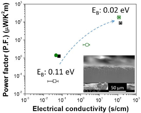
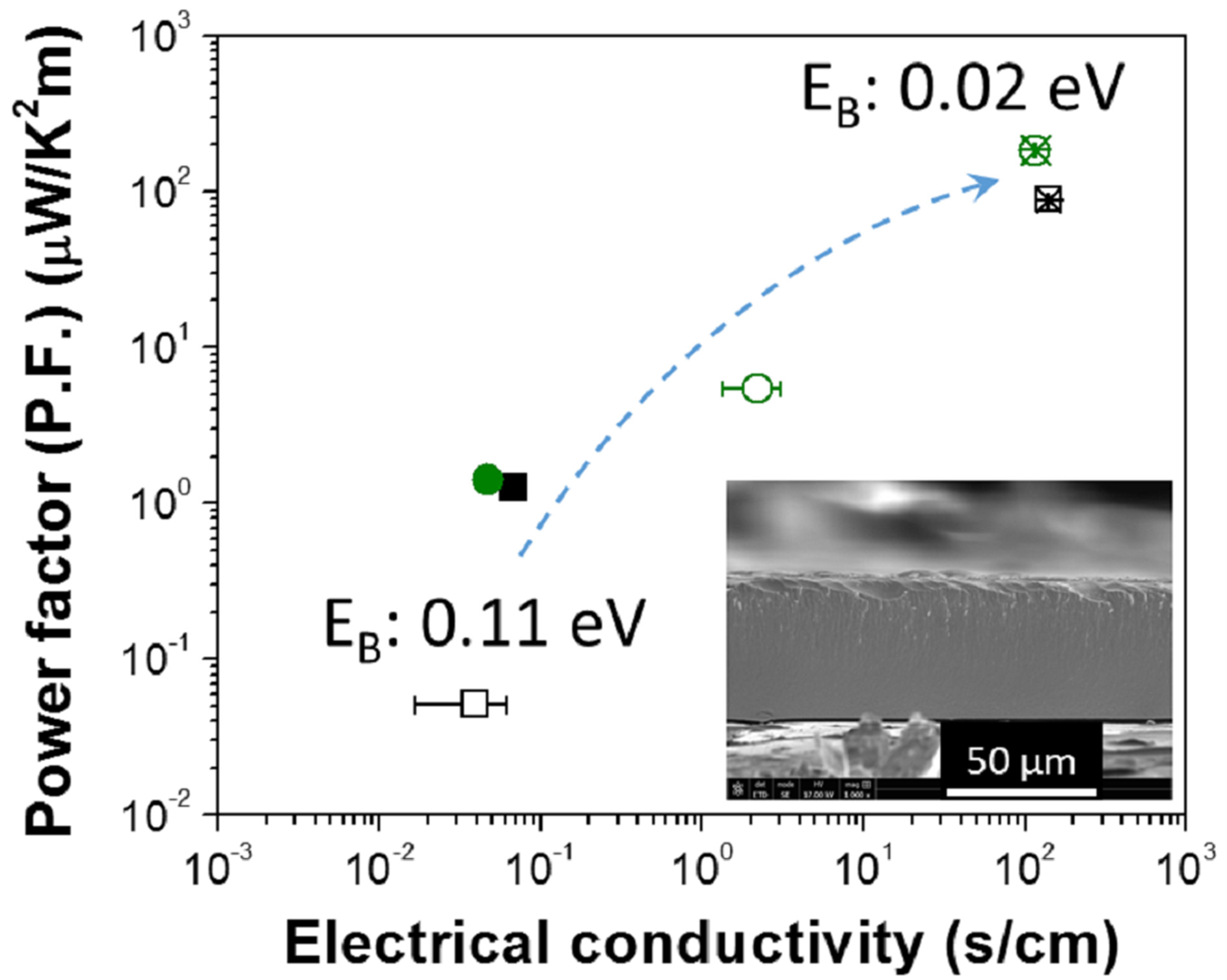
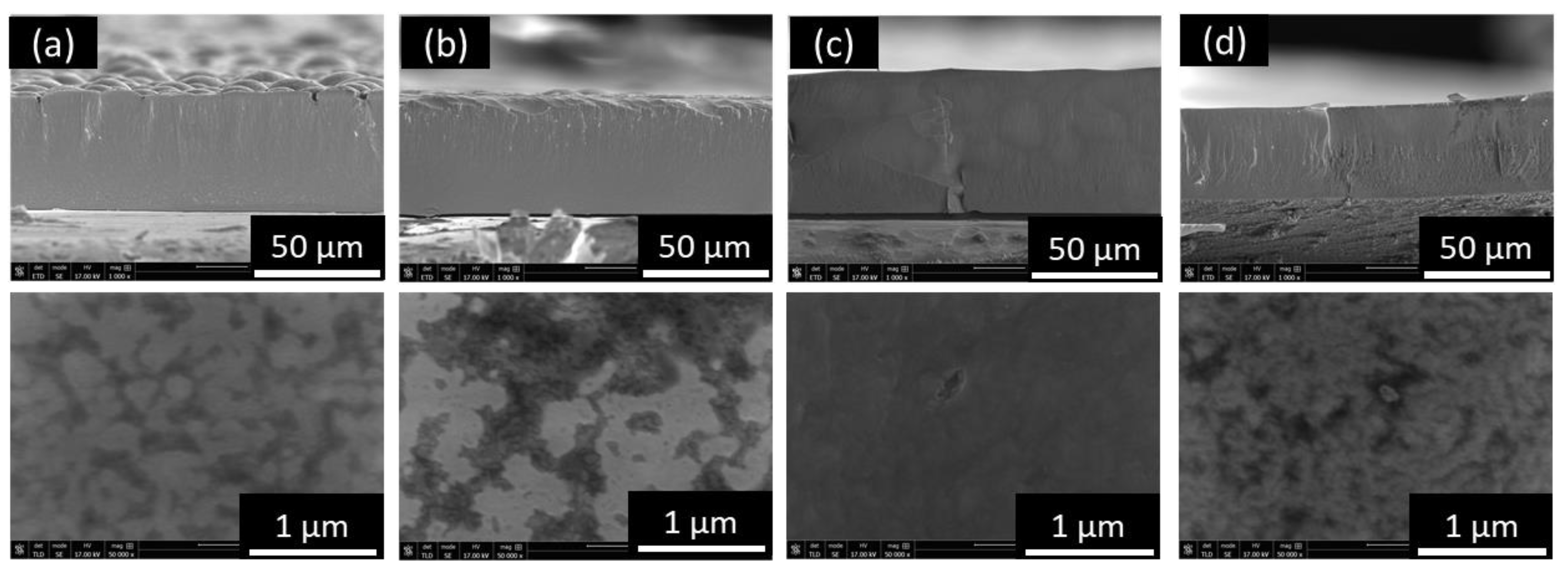
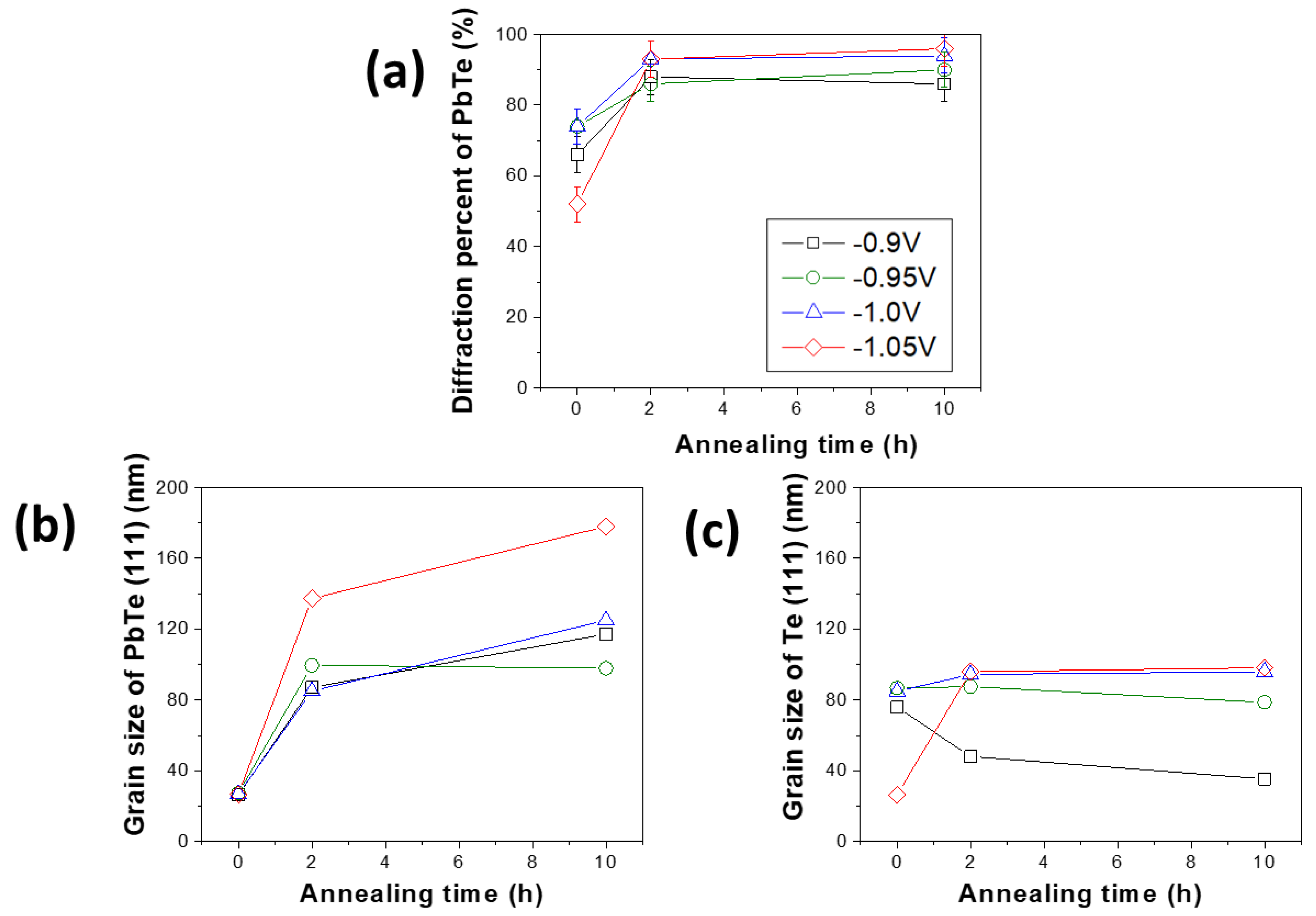
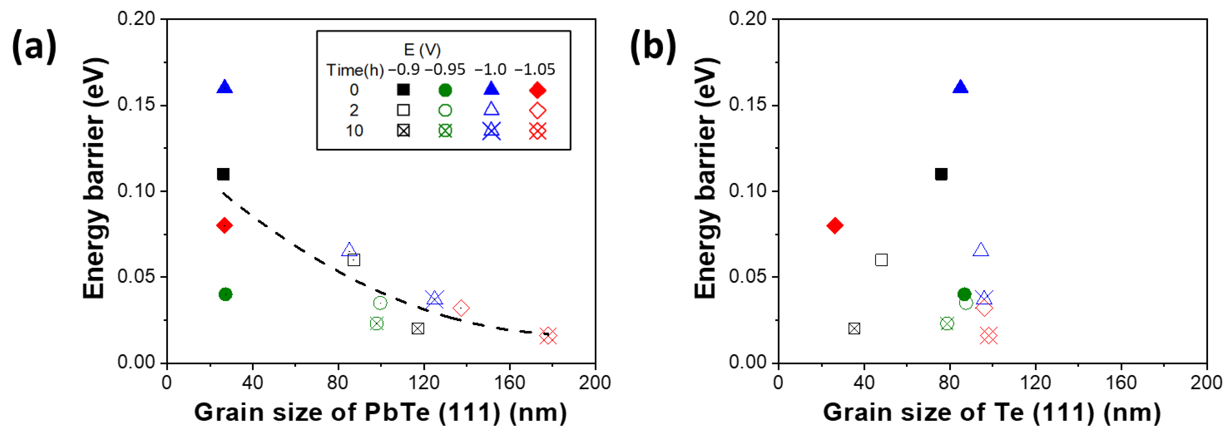
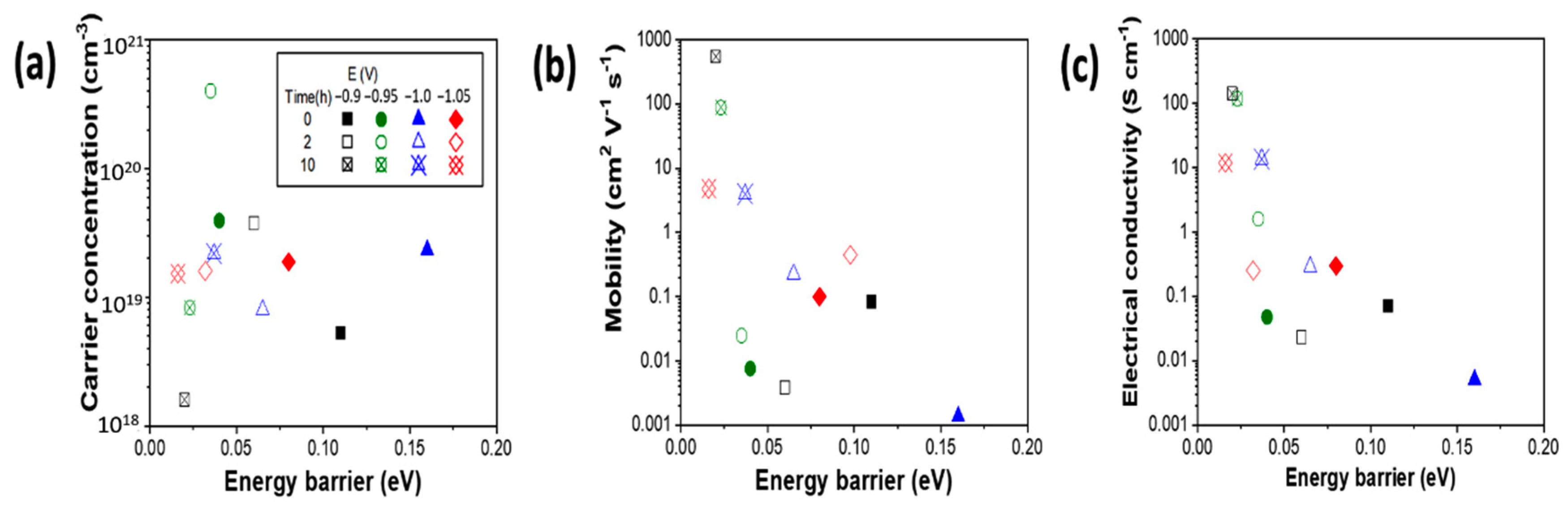
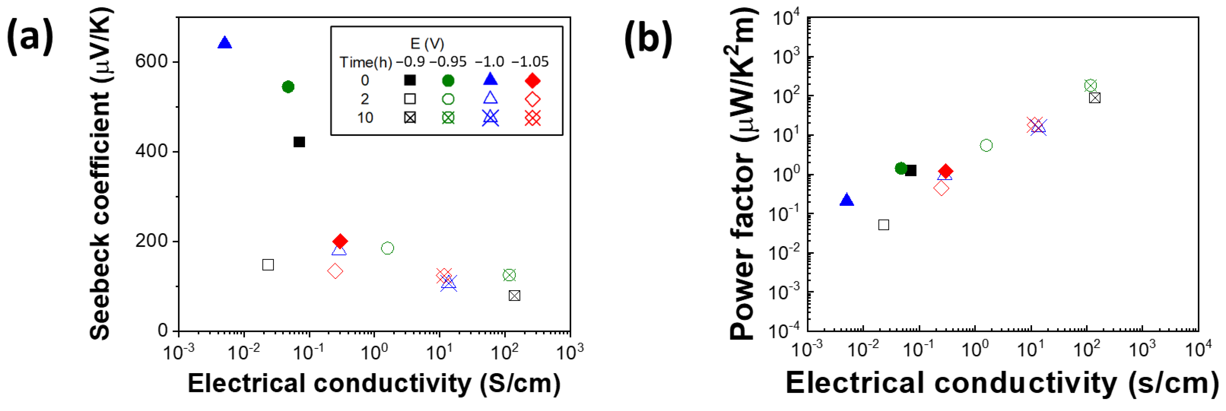
3. Results and Discussion

The four PbTe thick films (50 µm) were electrodeposited at different applied potentials resulting in different deposition rates (i.e., 115, 138, 167 and 163 µm/h), respectively. It is expected that the crystal structure and crystallinity would be different due to different growth rates. Additionally, the applied potential had effects not only on the growth rate, but also on the nucleation rate, where normally high overpotential results in high nucleation rates [40,41,42]. The nucleation rate of alloy as a function of applied overpotential have been expressed as the following equation:
d ln J d η = ( n A z A + n B z B + q ) e k T
where J is the nucleation rate, η is overpotential, nA and nB are number of atoms for element A and B, z is number of critical nuclei, q = αAzA or αBzB, α is ion transition coefficient, k is Boltzmann’s constant, T is temperature and e is elementary electric charge [42].
Based on this, the appropriate applied overpotential would lead to the films consisted of the small crystal size.
As shown in Figure 1, the four electrodeposited films are compact based on the cross-section SEM image (Figure 1a–d, top row) with slightly different surface morphology (Figure 1a–d, bottom row). At the applied potential of −0.90 and −0.95 V vs. sat. Ag/AgCl, the surface morphology is nodular (Figure 1a,b), while at the applied potential of −1.0 V vs. sat. Ag/AgCl (Figure 1c), the surface was smoother. Moreover, at the applied potential of −1.05 V the surface morphology became rougher, which may be caused by further reduction of Te at higher applied potential [36,43]. The composition of the four films determined by EDS analysis showed that it was independent of the applied potential (i.e., Pb content of 47 at.%) [36] due to under potential deposition (UPD) deposition mechanism [30,31].
The XRD patterns of as-deposited PbTe films are shown in Figure 2. Further adjustment of the crystallinity of the films were achieved by thermal treatment in a reductive atmosphere (i.e., 95 vol.% N2 + 5 vol.% H2). The thermal treatment process was carried out in a reductive atmosphere to prevent the oxidation of PbTe during the treatment. The annealing process was carried out at 200 °C for 2 and 10 h. The deposition rate increase from 120 to about 160 µm h−1 when applied potential changed from −0.9 to −1.05 V. According to Equation (1) and Buttler–Volmer’s equation, both nucleation rate and grain growth rate is enhanced dramatically by applied potential. Namely, the grain size of PbTe turned out to be almost the same with dominant crystal orientation of (111) (Figure 2) and nano-crystalline structure. For Tellurium, the preferred orientation is (111).
When the annealing process was carried out for 10 h, there was a contamination issue that the copper, which is a substrate material being used as the counter electrode, was diffused into the PbTe films electrodeposited −1.00 and −1.05 V (Figure S1a). However, PbTe samples electrodeposited at −0.90 and −0.95 V did not show copper diffusion (Figure S1a). The XRD patterns of the electrodeposited PbTe thick films match with the standard reference data (JCPDS-International Center for Diffraction Data, for Te No. 36-1452 and PbTe No. 38-1435). The un-indexed peak at 29.5 degree is attributed to the reflection of a frequency doubling radiation wave [44]. According to these XRD data, the electrodeposited films consisted of crystallized Te and PbTe with dominant orientation of (111) for both Te and PbTe phases. During the thermal treatment, the films were further crystallized which was identified by the decrease in FWHM of XRD peaks compared to as-deposited films. For the Te phase, because of its anisotropic hexagonal structure (i.e., six spiral chains at each corner and one in the center bound together via van der Waals forces) Te crystal normally has preferred orientation of (001) [45,46,47]. The fact that (111) orientation was dominant in Te crystal probably because it was surrounded by PbTe which had preferred orientation of (111). Two sets of information were extracted from the XRD data: one is the grain size of PbTe and Te, which is calculated by Scherrer equation [48], where the instrument peak broadening was corrected by substrate, and the stress-induced peak broadening from was corrected using Williamson–Hall analysis [49,50]; the other one is the quantitative information of crystalline PbTe and Te phases. This information was extracted by phase identification and estimation of the quantity of all identified phases of a mixture, which was realized using software (i.e., HighScore). The crystallite size and phase fraction of PbTe and Te, were plotted as a function of thermal treatment time (Figure 3). As the annealing time increased, the diffraction percentage of PbTe increased from 66 to 86% for the film electrodeposited at −0.9 V, 74 to 90% for the film electrodeposited at −0.95 V, 74 to 94% for the film electrodeposited at −1.0 V, and 52% to 96% for the film electrodeposited at −1.05 V. As expected, the average grain size of PbTe increased with increased in thermal treatment time. For example, the average grain size of PbTe increased from 26 to 117 nm (E = −0.9 V), 27 to 98 nm (E = −0.95 V), 26 to 125 nm (E = −1.0 V), and 27 to 178 nm (E = −1.05 V) respectively. However, the rate of increase of grain size decreased as an increase in annealing time. When the films were annealed for 2 h, the grain size of PbTe increased compared to as-deposit sample (i.e., from 26 to 117 nm for the film deposited at −0.9 V vs. Ag/AgCl, from 27 to 98 nm for the film deposited at −0.95 V vs. Ag/AgCl), from 27 to 85 nm for the film deposited at −1.0 V vs. Ag/AgCl), and from 27 to 137 nm for the film deposited at −0.95 V vs. Ag/AgCl); but when annealing time increased to 10 h, the increase of PbTe grain size was relatively small. At the same time, the grain size of Te phase decreased as the annealing time increased for the samples deposited at −0.9 and 0.95 V, for instance the grain size of Te decreased from 76 to 35 nm (E = −0.9 V) and 87 to 78 (E = −0.95 V) nm. This phenomenon contradicted with normal trend of grain size increase after the annealing. This may be caused by the evaporation of Te during the thermal treatment [51,52,53,54,55,56,57,58]. If this is the reason, after annealing the Te/(Te + Pb) ratio would decrease, however the data in Figure S1a showed that the Te/(Te + Pb) ratio remained constant, which indicated that Te evaporation is not the reason for the decrease of Te grain. The Ostwald ripening process, in which larger particles grow while smaller particles shrink, is a thermodynamically-driven spontaneous process because larger particles are more energetically stable [59,60,61]. In the Te-rich PbTe system, PbTe compound formation have a Gibbs free energy of −69.5 kJ/mol, which is thermodynamically favorable [62]. Moreover, Te has hexagonal crystal structure contains six spiral chains at each corner and one in the center, and the spiral chains are bound together via van der Waals forces [45], which are much weaker forces compared to chemical bond of Pb–Te. As a consequence, the possible explanation for decrease of Te grain size is that: the Te nanocrystal, which was relatively small amount, was embedded in the PbTe crystals, when the PbTe crystal grains started to growth, it may consume the Te atoms to fill its crystal imperfection and vacancy during the annealing process. Rojas-Chavez et al. also reported this phenomenon during PbTe milling. Their results show that during milling process, smaller particles and quantum dots are eventually dissolved completely to lower the total energy surface energy. They also mentioned that the formation of larger particles can be attributed to atom migration due to detachment of the atoms from amorphous zones [63].
For the two samples deposited at −1.0 and −1.05 V, Te grains increased slightly after annealing. In the nanocrystalline PbTe film, the dominant charge transfer mechanism would be significantly affected because its grain size changes as well as the interfaces as two different phases are formed. The energy barrier height of thick films was calculated using temperature-dependent electrical conductivity data (Figure S2) based on the Equation (2):
σ T 1 / 2 e x p [ E b k T ]
where σ is electrical conductivity, k is Boltzmann’s constant, T is temperature and Eb is energy barrier height [64,65]. The plot used to extract energy barrier height was shown in Figure S3. The energy barrier was influenced by grain size of the PbTe phase. According to literatures, the energy barrier from the dislocations at the grain boundaries can be ranged from 0.01 to 0.1 eV [66,67]. The difference of the initial energy barrier heights of the as-deposited films were distinctive (i.e., 0.11, 0.04, 0.16 and 0.08 eV for the film deposited at −0.9, −0.95, −1.0 and −1.05 V vs. Ag/AgCl, respectively as shown in Figure 4), which might be caused by crystal imperfection and vacancy formed at different growth rate (Figure 4). The difference in the energy barrier between samples became smaller after annealing (e.g., 0.02, 0.023, 0.037 and 0.016 eV for the film deposited at −0.9, −0.95, −1.0 and −1.05 V vs. Ag/AgCl, respectively, after annealed at 200 °C for 10 h). This is because the PbTe films tend to approach thermodynamically stable crystal structures after annealing so that the difference of energy barrier height of the films was diminished after annealing.
The carrier concentration, mobility and electrical conductivity as a function of energy barrier were plotted in Figure 5. The results showed that the carrier concentration does not have significant trend as a function of energy barrier height (Figure 5a). The increased carrier concentration of Te-embedded PbTe films can result from multiple reasons. For example, the excessed Te in the PbTe acted as acceptor, and the grain boundary may also contribute the increase of hole concentration [68]. Strauss et al. reported that the carrier concentration at of Te-saturated PbTe was typically about 3 × 1018 cm−3 and the maximum carrier concentration according to his data was 8 × 1018 cm−3, additionally he claimed that the carrier concentration of Te-saturated PbTe can barely go below 1017 cm−3 at room temperature, even after long-term annealing. [69] Allgaier et al. also reported the carrier concentration of p-type PbTe had a carrier concentration range of 4.85 × 10¹⁷ to 1.67 × 1019 cm−3 [70]. The mobility decreased significant as energy barrier increased (Figure 5b). The mobility can be presented by the following equations:
μ = L e [ 1 2 π m × k T ] 1 2 e x p ( E b k T )
where µ is mobility, L is grain size, e is elementary electric charge and m* is effective mass [64]. The relatively high mobility of 587 cm2 V−1 s−1 was achieved at low energy barrier range of about 0.02 eV, and the lowest mobility of 1.4 × 10⁻³ cm2·V−1 s−1 was obtained when energy barrier is 0.16 eV. Brebrick et al. reported that the hole mobility of Te rich PbTe was about 830 to 930 cm2·V−1 s−1 [71].
The electrical conductivity followed the same trend as mobility behavior when changing the energy barrier height, which can be expressed by following equation:
σ = L p e 2 [ 1 2 π × m k T ] 1 2 e x p ( E b k T )
where σ is electrical conductivity and p is average carrier concentration. Additionally, the Equations (3) and (4) was utilized base on the assumption that when Eb is not much smaller than kT [64]. According to the equation, the larger energy barrier height (Eb) leads to smaller electrical conductivity (σ). The best electrical conductivity (140 and 115 S cm−1) was achieved when the films showed the lowest energy barrier heights of about 0.02 eV for the films deposited at −0.9 and −0.95 V. The mobility and the electrical conductivity of the as-deposited sample at −0.9 V is larger than expected, which may be caused by a lower effective mass according to Equations (3) and (4). The as-deposited film at −0.9 V have an energy barrier of 0.11 eV, compared the samples have been annealed for 2 h with energy barrier of 0.06 eV, the as-deposited sample is supposed to have lower mobility and electrical conductivity. The bulk p-type PbTe has electrical conductivity higher than 103 S cm−1 at carrier concentration range of 1019 cm−3 at room temperature [72,73]. There are few studies reported the Cu doped PbTe. The results in this study showed that the thick films with Cu contamination have relatively high carrier concentration, and relatively low mobility and electrical conductivity. The two films deposited at −1.0 and −1.05 V have relatively low electrical conductivity (i.e., 13.7 and 11.7 S cm−1, respectively) after annealing for 10 h, which possibly because the formation of CuTe as a result of Cu diffusion during the annealing process. Introduction of the energy barrier by Te nano-inclusion and grain boundaries reduced the electrical conductivity of PbTe, which is consistent with the Equation (4). Compared to bulk Te-rich PbTe without other doping elements (Table 1), the electrodeposited Te-rich PbTe films have relatively high electrical conductivity and carrier concentration, but relatively low carrier mobility after annealing [38,39].
The Seebeck coefficient of four films were plotted as a function of the electrical conductivity. As shown in Figure 6a, the as-deposited films consisted of tens of nanometer-sized grains had the larger Seebeck coefficient values which is expected due to interdependency between Seebeck coefficient and electrical conductivity. As the films were annealed longer, the Seebeck coefficient decreased and the electrical conductivity increased at the same time. The calculated power factor (PF) showed the best values in the films annealed for 10 h where the films show the lowest barrier heights (Figure 6b). The highest power factor (183 μW K−2 m−1) was achieved at energy barrier of 0.023 eV. However, at even higher conductivity, Seebeck coefficient will decrease, hence the power factor will reach a peak and start decreasing. For the bulk p-type PbTe materials doped with 0.3% Na, the Seebeck coefficient is 120 µV K−1, and the electrical conductivity is about 2000 S cm−1 at room temperature [84]. Compared to the sample in this study, the Seebeck coefficient of the samples in the study is higher for the as-deposited thick films. However, the electrical conductivity of the thick films study in this study is lower than the bulk PbTe materials even after annealed for 10 h. Popescu et al. calculated the effect of the energy barrier on electrical conductivity, the results showed that higher energy barrier would result in lower electrical conductivity and lower Seebeck coefficient. Their results showed that the maximum thermoelectric power factor was achieved at the energy barrier of 0.095 eV [85]. Accordingly, in order to apply the nanocrysatlline PbTe thick films for thermoelectric applications, instead of the nano-inclusion of second phase, the engineering of grain size of single-phase PbTe films would be promising.

4. Conclusions

Nanocrystalline PbTe thick films were electrodeposited in alkaline solution with high deposition-rates (i.e., >100 µm/h). By adjusting the growth rate, the initial fraction of PbTe phase and its grain size were controlled whereas the formation of a secondary Te embedded phase was controlled by film composition. As-deposited PbTe thick films were thermal treated with a control of various temperature and duration to tailor the crystal structure and crystallinity. The thermoelectric properties (i.e., Seebeck coefficient and electrical conductivity, and power factor (PF)) of these films were measured at room temperature and correlated to their crystal structure, average grain size, and the fraction of Te phase. Additionally, the energy barrier heights (EB) were determined from the temperature dependent electrical conductivity. The highest PF of 183 μW K−2 cm−1 with a Seebeck coefficient of 125 µV K−1 and electrical conductivity of 116 S cm−1 were observed from Te embedded PbTe thick films with the average grain size of 100 nm.

Supplementary Materials

The following are available online at https://www.mdpi.com/2079-6412/11/3/356/s1, Figure S1. Cu content (a) and ration of Te/(Pb+Te) (b) as a function of annealing temperature for as-deposited and annealed (2 and 10 h) PbTe film deposited at −0.9, −0.95, −1.0, −1.05 V vs. Ag/AgCl; Figure S2. Electrical conductivity as a function of measurement temperature for as-deposited and annealed (2 and 10 h) PbTe film deposited at −0.9, −0.95, −1.0, −1.05 V vs. Ag/AgCl; Figure S3. Ln(σ*T1/2) as a function of 1/kT used to extract energy barrier height.

Author Contributions

Funding acquisition, J.-H.L. and K.-H.L.; Writing—original draft, T.W.; Writing—review & editing, J.K. and N.V.M. All authors have read and agreed to the published version of the manuscript.

Funding

This work was supported by the Global Frontier Program through the Global Frontier Hybrid Interface Materials (GFHIM) project of the National Research Foundation of Korea (NRF), funded by the R&D Center for Valuable Recycling (Global-Top R&BD Program) of the Ministry of Environment (ProjectNo.:2016002250005).

Institutional Review Board Statement

Not Applicable.

Informed Consent Statement

Not Applicable.

Data Availability Statement

Data is contained within the article or supplementary material.

Conflicts of Interest

The authors declare no conflict of interest.

References

  1. Curzon, F.L.; Ahlborn, B. Efficiency of a Carnot engine at maximum power output. Am. J. Phys. 1975, 43, 22–24. [Google Scholar] [CrossRef]
  2. Vining, C.B. An inconvenient truth about thermoelectrics. Nat. Mater. 2009, 8, 83–85. [Google Scholar] [CrossRef]
  3. Shakouri, A. Recent developments in semiconductor thermoelectric physics and materials. Annu. Rev. Mater. Res. 2011, 41, 399–431. [Google Scholar] [CrossRef]
  4. Snyder, G.J.; Toberer, E.S. Complex thermoelectric materials. Nat. Mater. 2008, 7, 105–114. [Google Scholar] [CrossRef]
  5. Poudel, B.; Hao, Q.; Ma, Y.; Lan, Y.; Minnich, A.; Yu, B.; Yan, X.; Wang, D.; Muto, A.; Vashaee, D.; et al. High-thermoelectric performance of nanostructured bismuth antimony telluride bulk alloys. Science 2008, 320, 634–638. [Google Scholar] [CrossRef] [PubMed] [Green Version]
  6. Faleev, S.V.; Léonard, F. Theory of enhancement of thermoelectric properties of materials with nanoinclusions. Phys. Rev. B 2008, 77. [Google Scholar] [CrossRef] [Green Version]
  7. Sumithra, S.; Takas, N.J.; Misra, D.K.; Nolting, W.M.; Poudeu, P.; Stokes, K.L. Enhancement in thermoelectric figure of merit in nanostructured Bi2Te3 with semimetal nanoinclusions. Adv. Energy Mater. 2011, 1, 1141–1147. [Google Scholar] [CrossRef]
  8. Chen, J.; Sun, T.; Sim, D.; Peng, H.; Wang, H.; Fan, S.; Hng, H.H.; Ma, J.; Boey, F.Y.C.; Li, S.; et al. Sb2Te3Nanoparticles with enhanced seebeck coefficient and low thermal conductivity. Chem. Mater. 2010, 22, 3086–3092. [Google Scholar] [CrossRef]
  9. Han, L.; Fang, H.; Du, C.; Sun, J.; Li, Y.; Ma, W. Synthesis of ultra-narrow PbTe nanorods with extremely strong quantum confinement. J. Mater. Sci. Technol. 2019, 35, 703–710. [Google Scholar] [CrossRef]
  10. Rojas-Chávez, H.; Juárez-García, J.; Herrera-Rivera, R.; Flores-Rojas, E.; González-Domínguez, J.; Cruz-Orea, A.; Cayetano-Castro, N.; Ávila-García, A.; Mondragón-Sánchez, M. The high-energy milling process as a synergistic approach to minimize the thermal conductivity of PbTe nanostructures. J. Alloys Compd. 2020, 820, 153167. [Google Scholar] [CrossRef]
  11. Hsieh, H.-C.; Wang, C.-H.; Lan, T.-W.; Lee, T.-H.; Chen, Y.-Y.; Chu, H.-S.; Wu, A.T. Joint properties enhancement for PbTe thermoelectric materials by addition of diffusion barrier. Mater. Chem. Phys. 2020, 246, 122848. [Google Scholar] [CrossRef]
  12. Ohta, M.; Jood, P.; Murata, M.; Lee, C.-H.; Yamamoto, A.; Obara, H. An integrated approach to thermoelectrics: Combining phonon dynamics, nanoengineering, novel materials development, module fabrication, and metrology. Adv. Energy Mater. 2018, 9, 1–29. [Google Scholar] [CrossRef]
  13. Novak, T.G.; Kim, K.; Jeon, S. 2D and 3D nanostructuring strategies for thermoelectric materials. Nanoscale 2019, 11, 19684–19699. [Google Scholar] [CrossRef]
  14. Fleurial, J.-P.; Snyder, G.J.; Herman, J.A.; Giauque, P.H. Thick-film thermoelectric microdevices. In Proceedings of the Eighteenth International Conference on Thermoelectrics, Baltimore, MD, USA, 29 August–2 September 1999. [Google Scholar]
  15. Semeniouk, V.; Fleurial, J.-P. Modeling and minimization of intercascade thermal resistance in multi-stage thermoelectric cooler. In Proceedings of the XVI International Conference on Thermoelectrics, Dresden, Germany, 26–29 August 1997. [Google Scholar]
  16. Anatychuk, L.; Luste, O.; Vikhor, L. Optimal functions as an effective method for thermoelectric devices design. In Proceedings of the Fifteenth International Conference on Thermoelectrics, Pasadena, CA, USA, 26–29 March 1996; pp. 223–226. [Google Scholar]
  17. Anatychuk, L.I.; Luste, O.J. Physical principles of microminiaturization in thermoelectricity. In Proceedings of the Fifteenth International Conference on Thermoelectrics, Pasadena, CA, USA, 26–29 March 1996. [Google Scholar]
  18. Snyder, G.J.; Lim, J.R.; Huang, C.-K.; Fleurial, J.-P. Thermoelectric microdevice fabricated by a MEMS-like electrochemical process. Nat. Mater. 2003, 2, 528–531. [Google Scholar] [CrossRef]
  19. Dini, J.W. Electrodeposition—The Materials Science of Coating and Substrates; Noyes Publications: Westwood, NJ, USA, 1993. [Google Scholar]
  20. Rostek, R.; Stein, N.; Boulanger, C. A review of electroplating for V–VI thermoelectric films: From synthesis to device integration. J. Mater. Res. 2015, 30, 2518–2543. [Google Scholar] [CrossRef]
  21. Xiao, F.; Hangarter, C.; Yoo, B.; Rheem, Y.; Lee, K.-H.; Myung, N.V. Recent progress in electrodeposition of thermoelectric thin films and nanostructures. Electrochim. Acta 2008, 53, 8103–8117. [Google Scholar] [CrossRef]
  22. Beaunier, L.; Cachet, H.; Cortes, R.; Froment, M. Epitaxial electrodeposition of lead telluride films on indium phosphide single crystals. J. Electroanal. Chem. 2002, 532, 215–218. [Google Scholar] [CrossRef]
  23. Li, G.-R.; Yao, C.-Z.; Lu, X.-H.; Zheng, F.-L.; Feng, Z.-P.; Yu, X.-L.; Su, C.-Y.; Tong, Y.-X. Facile and efficient electrochemical synthesis of PbTe dendritic structures. Chem. Mater. 2008, 20, 3306–3314. [Google Scholar] [CrossRef]
  24. Ni, Y.; Zhang, Y.; Hong, J. Potentiostatic electrodeposition route for quick synthesis of featherlike PbTe dendrites: Influencing factors and shape evolution. Cryst. Growth Des. 2011, 11, 2142–2148. [Google Scholar] [CrossRef]
  25. Mondal, A.; Mukherrjee, N.; Bhar, S.; Banerjee, D. An electrochemical technique to deposit thin films of PbTe. Thin Solid Film. 2006, 515, 1255–1259. [Google Scholar] [CrossRef]
  26. Li, X.; Nandhakumar, I.S. Direct electrodeposition of PbTe thin films on n-type silicon. Electrochem. Commun. 2008, 10, 363–366. [Google Scholar] [CrossRef]
  27. Ivanova, Y.A.; Ivanou, D.K.; Streltsov, E.A. Electrochemical deposition of PbTe onto n-Si(100) wafers. Electrochem. Commun. 2007, 9, 599–604. [Google Scholar] [CrossRef]
  28. Xiao, F.; Yoo, B.; Ryan, M.A.; Lee, K.-H.; Myung, N.V. Electrodeposition of PbTe thin films from acidic nitrate baths. Electrochim. Acta 2006, 52, 1101–1107. [Google Scholar] [CrossRef]
  29. Pourbaix, M. Atlas of Electrochemical Equilibria in Aqueous Solutions; Pergamon Press Inc.: Long Island City, NY, USA, 1966. [Google Scholar]
  30. Saloniemi, H.; Kanniainen, T.; Ritala, M.; Leskelä, M. Electrodeposition of PbTe thin films. Thin Solid Films 1998, 326, 78–82. [Google Scholar] [CrossRef]
  31. Saloniemi, H.; Kemell, M.; Ritala, M.; Leskelä, M. PbTe electrodeposition studied by combined electrochemical quartz crystal microbalance and cyclic voltammetry. J. Electroanal. Chem. 2000, 482, 139–148. [Google Scholar] [CrossRef]
  32. Miranda, C.R.B.; Abramof, P.G.; De Melo, F.C.L.; Ferreira, N.G. Morphology and stress study of nanostructured porous silicon as a substrate for PbTe thin films growth by electrochemical process. Mater. Res. 2004, 7, 619–623. [Google Scholar] [CrossRef] [Green Version]
  33. Qiu, X.; Lou, Y.; Samia, A.C.S.; Devadoss, A.; Burgess, J.D.; Dayal, S.; Burda, C. PbTe Nanorods by Sonoelectrochemistry. Angew. Chem. Int. Ed. 2005, 44, 5855–5857. [Google Scholar] [CrossRef]
  34. Erdoğan, İ.Y.; Ozer, T.O.; Bülbül, F.; Demir, Ü. Characterization of size-quantized PbTe thin films synthesized by an electrochemical co-deposition method. Thin Solid Films 2009, 517, 5419–5424. [Google Scholar] [CrossRef]
  35. Butler, I.B.; Schoonen, M.A.A.; Rickard, D.T. Removal of dissolved oxygen from water: A comparison of four common techniques. Talanta 1994, 41, 211–215. [Google Scholar] [CrossRef]
  36. Wu, T.; Lee, H.-K.; Myung, N.V. Electrodeposition of dense lead telluride thick films in alkaline solutions. J. Electrochem. Soc. 2016, 163, D801–D808. [Google Scholar] [CrossRef]
  37. Yoo, I.-J.; Song, Y.; Lim, D.C.; Myung, N.V.; Lee, K.H.; Oh, M.; Lee, D.; Kim, Y.D.; Kim, S.; Choa, Y.-H.; et al. Thermoelectric characteristics of Sb2Te3 thin films formed via surfactant-assisted electrodeposition. J. Mater. Chem. A 2013, 1, 5430–5435. [Google Scholar] [CrossRef]
  38. Kim, J.; Zhang, M.; Bosze, W.; Park, S.-D.; Lim, J.-H.; Myung, N.V. Maximizing thermoelectric properties by nanoinclusion of γ-SbTe in Sb2Te3 film via solid-state phase transition from amorphous Sb–Te electrodeposits. Nano Energy 2015, 13, 727–734. [Google Scholar] [CrossRef]
  39. Kim, J.; Lee, K.H.; Kim, S.-D.; Lim, J.-H.; Myung, N.V. Simple and effective fabrication of Sb2Te3 films embedded with Ag2Te nanoprecipitates for enhanced thermoelectric performance. J. Mater. Chem. A 2017, 6, 349–356. [Google Scholar] [CrossRef]
  40. Mostany, J.; Scharifker, B.R.; Saavedra, K.; Borras, C. Electrochemical nucleation and the classical theory: Overpotential and temperature dependence of the nucleation rate. Russ. J. Electrochem. 2008, 44, 652–658. [Google Scholar] [CrossRef]
  41. Moti’, E.; Shariat, M.H.; Bahrololoom, M.E. Influence of cathodic overpotential on grain size in nanocrystalline nickel deposition on rotating cylinder electrodes. J. Appl. Electrochem. 2008, 38, 605–612. [Google Scholar] [CrossRef]
  42. Milchev, A.; Lacmann, R. On the nucleation theory of electrochemical alloy formation I. overvoltage dependence of the stationary nucleation rate. J. Cryst. Growth 1991, 110, 919–924. [Google Scholar] [CrossRef]
  43. Wu, T.; Zhang, M.; Lee, K.-H.; Lee, C.-M.; Lee, H.-K.; Choa, Y.; Myung, N.V. Electrodeposition of compact tellurium thick films from alkaline baths. J. Electrochem. Soc. 2016, 164, D82–D87. [Google Scholar] [CrossRef]
  44. Mo, M.; Zeng, J.; Liu, X.; Yu, W.; Zhang, S.; Qian, Y. Controlled hydrothermal synthesis of thin single-crystal tellurium nanobelts and nanotubes. Adv. Mater. 2002, 14, 1658–1662. [Google Scholar] [CrossRef]
  45. Hippel, G.A.v. Structure, conductivity in the VIb group of the periodic system. J. Chem. Phys. 1948, 16, 372–380. [Google Scholar] [CrossRef]
  46. Wu, T.; Zhang, M.; Lee, K.-H.; Kim, S.-I.; Choa, Y.; Myung, N.V. Synthesis of tellurium heterostructures by galvanic displacement reaction of zinc in alkaline baths. Electrochim. Acta 2014, 150, 298–307. [Google Scholar] [CrossRef]
  47. Wu, T.; Myung, L.Y.; Zhang, M.; Lee, K.-H.; Lee, Y.L.; Lim, H.-R.; Kim, B.S.; Choa, Y.-H.; Myung, N.V. Size controlled synthesis of tellurium nanorices by galvanic displacement reaction of aluminum. Electrochim. Acta 2015, 176, 1382–1392. [Google Scholar] [CrossRef]
  48. Patterson, A.L. The scherrer formula for X-ray particle size determination. Phys. Rev. 1939, 56, 978–982. [Google Scholar] [CrossRef]
  49. Williamson, G.; Hall, W. X-ray line broadening from filed aluminium and wolfram. Acta Met. 1953, 1, 22–31. [Google Scholar] [CrossRef]
  50. Burton, A.W.; Ong, K.; Rea, T.; Chan, I.Y. On the estimation of average crystallite size of zeolites from the Scherrer equation: A critical evaluation of its application to zeolites with one-dimensional pore systems. Microporous Mesoporous Mater. 2009, 117, 75–90. [Google Scholar] [CrossRef]
  51. Weidmann, E.; Anderson, J. Structure and growth of oriented tellurium thin films. Thin Solid Films 1971, 7, 265–276. [Google Scholar] [CrossRef]
  52. Sciences, C. Large grain tellurium thin films. Thin Solid Films 1972, 11, 229–236. [Google Scholar]
  53. Santucci, S.; Di Nardo, S.; Lozzi, L.; Passacantando, M.; Picozzi, P. XPS, LEED and AFM investigation of the Si(100) surface after the deposition and annealing of tellurium thin films. Surf. Sci. 1996, 352–354, 1027–1032. [Google Scholar] [CrossRef]
  54. Bhandarkar, V.; Sen, S.; Muthe, K.; Kaur, M.; Kumar, M.S.; Deshpande, S.; Gupta, S.; Yakhmi, J.V.; Sahni, V. Effect of deposition conditions on the microstructure and gas-sensing characteristics of Te thin films. Mater. Sci. Eng. B 2006, 131, 156–161. [Google Scholar] [CrossRef]
  55. Kim, D.-H.; Lee, G.-H. Effect of rapid thermal annealing on thermoelectric properties of bismuth telluride films grown by co-sputtering. Mater. Sci. Eng. B 2006, 131, 106–110. [Google Scholar] [CrossRef]
  56. Rostek, R.; Sklyarenko, V.; Woias, P. Influence of vapor annealing on the thermoelectric properties of electrodeposited Bi2Te3. J. Mater. Res. 2011, 26, 1785–1790. [Google Scholar] [CrossRef]
  57. Kim, D.H.; Kwon, I.H.; Kim, C.; Han, B.; Im, H.J.; Kim, H. Tellurium-evaporation-annealing for p -type bismuth—Antimony—Telluride thermoelectric materials. J. Alloys Compd. 2013, 548, 126–132. [Google Scholar] [CrossRef]
  58. Zalar, S.M. High-Temperature Resistivity of the Chalcopyritic Compound CulnTe2. J. Electrochem. Soc. 1966, 113, 230. [Google Scholar] [CrossRef]
  59. Ostwald, W. Studies on the formation and transformation of solid bodies. Z. Phys. Chem. 1897, 22, 289–330. [Google Scholar]
  60. McNaught, A.D.; Wilkinson, A. Compendium of Chemical Terminology; International Union of Pure and Applied Chemistry: Raleigh, NC, USA, 1997. [Google Scholar]
  61. Ratke, L.; Voorhees, P.W. Growth and Coarsening Ostwald Ripening in Material Processing; Springer: Berlin, Germany, 2002. [Google Scholar]
  62. CRC Handbook of Chemistry and Physics; CRC Press: Boca Raton, FL, USA, 2002.
  63. Rojas-Chávez, H.; Cruz-Martínez, H.; Flores-Rojas, E.; Juárez-García, J.M.; Gonzalez-Dominguez, J.L.; Daneu, N.; Santoyo-Salazar, J.; Santoyo, J. The mechanochemical synthesis of PbTe nanostructures: Following the Ostwald ripening effect during milling. Phys. Chem. Chem. Phys. 2018, 20, 27082–27092. [Google Scholar] [CrossRef] [PubMed]
  64. Seto, J.Y.W. The electrical properties of polycrystalline silicon films. J. Appl. Phys. 1975, 46, 5247–5254. [Google Scholar] [CrossRef]
  65. Scheele, M.; Oeschler, N.; Veremchuk, I.; Peters, S.-O.; Littig, A.; Kornowski, A.; Klinke, C.; Weller, H. Thermoelectric properties of lead chalcogenide core–shell nanostructures. ACS Nano 2011, 5, 8541–8551. [Google Scholar] [CrossRef] [Green Version]
  66. Kishimoto, K.; Yamamoto, K.; Koyanagi, T. Influences of potential barrier scattering on the thermoelectric properties of sintered n-Type PbTe with a small grain size. Jpn. J. Appl. Phys. 2003, 42, 501–508. [Google Scholar] [CrossRef]
  67. Kishimoto, K.; Koyanagi, T. Preparation of sintered degenerate n-type PbTe with a small grain size and its thermoelectric properties. J. Appl. Phys. 2002, 92, 2544. [Google Scholar] [CrossRef]
  68. Schenk, M.; Berger, H.; Klimakow, A.; Mühlberg, M.; Wienecke, M. Nonstoichiometry and point defects in PbTe. Cryst. Res. Technol. 1988, 23, 77–84. [Google Scholar] [CrossRef]
  69. Strauss, A.J. Effect of Pb- and Te-saturation on carrier concentrations in impurity-doped PbTe. J. Electron. Mater. 1973, 2, 553–569. [Google Scholar] [CrossRef]
  70. Allgaier, R.S. Valence bands in lead telluride. J. Appl. Phys. 1961, 32, 2185. [Google Scholar] [CrossRef]
  71. Brebrick, R.F.; Gubner, E. Composition stability limits of PbTe. II. J. Chem. Phys. 1962, 36, 1283–1289. [Google Scholar] [CrossRef]
  72. Fritts, R.W. Thermoelectric Materials and Devices; Reinhold Publication Corporation: New York, NY, USA, 1960; pp. 143–162. [Google Scholar]
  73. LaLonde, A.D.; Pei, Y.; Wang, H.; Snyder, G.J. Lead telluride alloy thermoelectrics. Mater. Today 2011, 14, 526–532. [Google Scholar] [CrossRef]
  74. Shogenji, K.; Uchiyama, S. On electrical resistivity and hall coefficient of PbTe crystals. J. Phys. Soc. Jpn. 1957, 12, 252–258. [Google Scholar] [CrossRef]
  75. Allgaier, R.S.; Scanlon, W.W. Mobility of electrons and holes in PbS, PbSe, and PbTe between room temperature and 4.2 °K. Phys. Rev. 1958, 111, 1029–1037. [Google Scholar] [CrossRef]
  76. Miller, E.; Komarek, K.; Cadoff, I. Interrelation of electronic properties and defect equilibria in PbTe. J. Appl. Phys. 1961, 32, 2457–2465. [Google Scholar] [CrossRef]
  77. Scanlon, W.W. Precipitation of Te and Pb in PbTe crystals. Phys. Rev. 1962, 126, 509–513. [Google Scholar] [CrossRef]
  78. Crocker, A.J.; Rogers, L.M. Interpretation of the Hall coefficient, electrical resistivity and Seebeck coefficient of p-type lead telluride. Br. J. Appl. Phys. 1967, 18, 563–573. [Google Scholar] [CrossRef]
  79. Das, V.D.; Bhat, K.S. Anomalous temperature dependence of thermoelectric power of PbTe thin films. J. Appl. Phys. 1983, 54, 6641. [Google Scholar] [CrossRef]
  80. Heremans, J.P.; Thrush, C.M.; Morelli, D.T. Thermopower enhancement in lead telluride nanostructures. Phys. Rev. B 2004, 70, 115334. [Google Scholar] [CrossRef]
  81. Martin, J.; Wang, L.; Chen, L.; Nolas, G.S. Enhanced Seebeck coefficient through energy-barrier scattering in PbTe nanocomposites. Phys. Rev. B 2009, 79, 115311. [Google Scholar] [CrossRef] [Green Version]
  82. Bagiyeva, G.Z.; Mustafayev, N.B.; Abdinova, G.D.; Abdinov, D.S. Electrical properties of PbTe single crystals with excess tellurium. Semiconductors 2011, 45, 1391–1394. [Google Scholar] [CrossRef]
  83. Rawat, P.K.; Paul, B.; Banerji, P. Lead telluride based thermoelectrics: Approaches for higher efficiency. In Materials and Processes for Energy: Communicating Current Research and Technological Developments; Formatex Research Center: Badajoz, Spain, 2013; Volume 1, pp. 840–851. [Google Scholar]
  84. Wright, D.A. Materials for direct-conversion thermoelectric generators. Metallurg. Rev. 1970, 15, 147–160. [Google Scholar]
  85. Popescu, A.; Woods, L.M.; Martin, J.; Nolas, G.S. Model of transport properties of thermoelectric nanocomposite materials. Phys. Rev. B 2009, 79, 205302. [Google Scholar] [CrossRef] [Green Version]
Figure 1. SEM images of PbTe electrodeposited at different applied potential: (a) −0.9, (b) −0.95, (c) −1.0, and (d) −1.05 V with 550 mM (TeO32−), 100 mM (Pb2+), and (EDTA4−)/(Pb2+) of 7.5 at pH of 12.3 and temperature of 23 °C. The top row im-ages are cross-section view, and the bottom row images are top view. Pb content of the four samples are 47%.
Coatings 11 00356 g001
Figure 2. XRD analysis of as deposited and annealed at 200 °C for 2 and 10 h. The PbTe films were electrodeposited at different applied potential of (a) −0.9, (b) −0.95, (c) −1.0 and (d) −1.05 V with 550 mM (TeO32−), 100 mM (Pb2+), and [EDTA4−]/[Pb2+] of 7.5 at pH of 12.3 and temperature of 23 °C.
Coatings 11 00356 g002
Figure 3. Diffraction percent (a) and grain size of PbTe (b), grain size of Te (c) as a function of annealing time (0, 2 and 10 h). The PbTe film electrodeposited at different applied potential: −0.9, −0.95, −1.0 and −1.05 V with 550 mM (TeO32−), 100 mM (Pb2+), and (EDTA4−)/(Pb2+) of 7.5 at pH of 12.3 and temperature of 23 °C.
Coatings 11 00356 g003
Figure 4. Change of energy barrier (EB) of as-deposited and annealed PbTe films at 200 °C for 2 and 10 h as a function of grain size of PbTe phase (a) and Te phase (b).
Coatings 11 00356 g004
Figure 5. Carrier concentration (a), mobility (b) and electrical conductivity (c) as a function of energy barrier (EB) of as-deposited and annealed PbTe films at 200 °C for 2 and 10 h.
Coatings 11 00356 g005
Figure 6. Seebeck coefficient (a) and power factor (PF) (b) of as-deposited and annealed PbTe films at 200 °C for 2 and 10 h as a function of electrical conductivity.
Coatings 11 00356 g006
Table 1. Summary of electrical and thermoelectric properties of Te-rich PbTe.
Ref.YearGrain SizeS (µV K−1)σ (S cm−1)PF (µW K−2 m−1)κ (W m−1 K−1)p (1019 cm−3)µ (cm2 V−1 s−1)
[74]195725500
[75]19583290.302724
[76]196126040560
[70]19610.0048–1.67
[77]196244017.23330.015715
42024.44300.019790
37038.55270.033730
34052.66080.048690
290109.99240.100680
[78]1967400629920.043900
[69]1973 0.4–0.8
[79]1983350–470
[68]1988 0.2–1.2
[80]2004≥60 nm4060.038
44 nm4560.046
42 nm5086.71730.021
4940.014
36 nm18922.2790.820
1740.760
2650.220
[81]2009316 nm32840.24322.20.095
396 nm32479.48342.50.150
[82]201118025.181
30052.5473
[83]201333025280
31550500
30583780
Publisher’s Note: MDPI stays neutral with regard to jurisdictional claims in published maps and institutional affiliations.

