Article

Compositional, Structural, Morphological, and Optical Properties of ZnO Thin Films Prepared by PECVD Technique

by
Noureddine Hacini
1,2,
Mostefa Ghamnia
1,*,
Mohamed Amine Dahamni
1,
Abdelwaheb Boukhachem
3,
Jean-Jacques Pireaux
2 and
Laurent Houssiau
2
1
Laboratoire des Sciences de la Matière Condensée (LSMC), Université Oran 1 Ahmed Ben Bella, Oran 31100, Algeria
2
LISE Laboratory, (NISM-LISE), Namur Institute of Structured Matter, Université de Namur, 5000 Namur, Belgium
3
Unité de Physique des Dispositifs à Semi-conducteurs, Faculté des Sciences de Tunis, Université de Tunis El Manar, Tunis 2092, Tunisia
*
Author to whom correspondence should be addressed.
Coatings 2021, 11(2), 202; https://doi.org/10.3390/coatings11020202
Submission received: 21 December 2020 / Revised: 25 January 2021 / Accepted: 28 January 2021 / Published: 10 February 2021

Abstract

:
ZnO thin films were synthesized on silicon and glass substrates using the plasma-enhanced chemical vapor deposition (PECVD) technique. Three samples were prepared at substrates temperatures of 200, 300, and 400 °C. The surface chemical composition was analyzed by the use of X-Ray Photoelectron spectroscopy (XPS). Structural and morphological properties were studied by using X-ray diffraction (XRD) and scanning electron microscopy (SEM). Optical properties were carried out by UV-visible spectroscopy. XPS spectra showed typical peaks of Zn(2p3/2), Zn(2p1/2), and O(1s) of ZnO with a slight shift attributed to the substrate temperature. XRD analysis revealed hexagonal wurtzite phases with a preferred (002) growth orientation that improved with temperature. Calculation of grain size and dislocation density revealed the crystallization improvement of ZnO when the substrate temperature varied from 200 to 400 °C. SEM images of ZnO films showed textured surfaces composed of grains of spherical shape uniformly distributed. The transmittance yields are reaching 80%, and the values of the band-gap energy indicate that the ZnO films prepared by PECVD present transparent and semiconducting properties.

1. Introduction

Many works have focused on the study of zinc oxide (ZnO) material, because it is one of the most interesting transparent conducting oxide (TCO) materials. The number of articles published on ZnO is increasing every year, and it is becoming a semiconductor as important as silicon. The advantages of ZnO are numerous: it is a non-toxic material, in abundance in nature and of low cost. ZnO is a II–VI compound semiconductor with a wide direct band gap (3.2–3.4 eV) [1,2,3,4,5] and a large exciton binding energy (60 meV) at room temperature [6,7,8] that is 3 times the binding energy of ZnS (20 meV) and 2.4 times the one of GaN (25 meV) [9,10]. These characteristics make it useful in various fields such as transparent conductive films, solar cells, photoconductors, and luminescent devices [11,12,13]. Therefore, ZnO is used in numerous applications in optoelectronics devices such as UV-laser diodes, light-emitting diodes, thin films transistors, etc. [14,15]. For these applications, ZnO should exhibit both high electrical conductivity and high optical transparency in the visible region. The pioneers of zinc oxide synthesis have succeeded in using this material as a window for silicon-based solar cells [16,17,18]. Due to these promising properties, we were interested in the synthesis and growth of ZnO thin nanostructured films, which can increase their electrical properties [19,20,21]. ZnO nanostructured films can be obtained by several methods which can be of physical type such as radio frequency magnetron sputtering [22,23], electron beam evaporation [24,25], pulsed laser deposition [26,27], molecular beam epitaxy (MBE) [28,29], or of chemical type as spin coating [30,31], dip coating [32,33], spray pyrolysis [34,35], chemical vapor deposition (CVD) [36,37] and plasma-enhanced chemical vapor deposition (PECVD) [38,39]. Out of these, PECVD is of particular interest due to its simplicity, lack of need for ultra-high vacuum requirement, and its capability of deposing films of good crystalline quality. In this regard, we report the synthesis and characterization of ZnO nanostructured films, deposited on silicon and glass substrates by the PECVD method. In this study, we report the synthesis and characterization of ZnO thin films deposited on silicon and glass substrates heated at 200, 300, and 400 °C. The goal of such study is to synthesize good ZnO films for the fabrication of window coatings for light detecting.

2. Experimental Part

ZnO nanostructured films were deposited on silicon (100) and glass substrates by plasma-enhanced chemical vapor deposition (PECVD). The precursor used in this study was zinc acetylacetonate Zn(acac)2 of chemical formula (Zn(C5H7O2)2, xH2O)2 99.99% purity purchased from Sigma Aldrich. The Zn(acac)2 powder was sublimated at 150 °C using a temperature controlled resistive heater. The obtained vapor was entered into plasma chamber using Ar as carrier gas at a 4 sccm flux. Dioxygen O2 was also introduced in the plasma chamber at 20 sccm. The gas flows were controlled with a Multi Gas Controller 647C from MKS (Munich, Germany). The Zn(acac)2 vapor mixed with Ar was injected near the substrates with a small ring shower (about 5 cm diameter). The plasma was generated with a planar helicoidal inductive coupling plasma source (ICP) from Plasma Consult (ICP-P-200, Nano_Master Inc, Austin, USA) operated at 13.56 MHz. The plasma power was fixed at 250 W and controlled with a Cesar RF Power Generator from Dressler (Stolberg Vicht, Germany). The decomposition under plasma discharge and reaction with oxygen takes place on heated substrate surfaces to form the ZnO films. The pressure inside the plasma chamber during deposition varied with the substrate temperature and was 1.24 Torr (165 Pa) at 200 °C, 2.15 Torr (286 Pa) at 300 °C, and 3.31 Torr (440 Pa) at 400 °C. The Zn(acac)2 vapor mixed with Ar was injected near the substrates with a small ring shower (about 5 cm diameter). The quality of the deposits depends on several parameters; among them, the temperature of the substrates, the pressure in the reaction chamber, and the flow rates of the argon and oxygen gases.
The selected substrates were silicon (001) for structural, morphological, and compositional characterization, and glass substrates for the optical study. To avoid any contamination with the film deposit, the substrates surfaces have undergone cleaning cycles using acetone, methanol, and deionized water in an ultrasonic bath for 10 min and ended by blowing with nitrogen gas to dry them. Our study focused on three types of samples indicated in Table 1.
These samples characterizations were carried out using X-ray photoelectron spectroscopy (XPS, K-Alpha from Thermo Scientific Instruments, East Grinstead, UK) for chemical composition analysis, X-ray diffraction (XRD, X’Pert PRO from PANalytical B. V. (Almelo, The Netherlands) using copper line of wavelength λ = 1.54 Å), and scanning electron microscopy (SEM, JEOL 7500-F, Tokyo, Japan) for the structural and morphological study and UV-visible spectroscopy for optical properties. The ZnO films thicknesses were not measured but estimated as several hundred nm (thick whitish deposit).

3. Results and Discussion

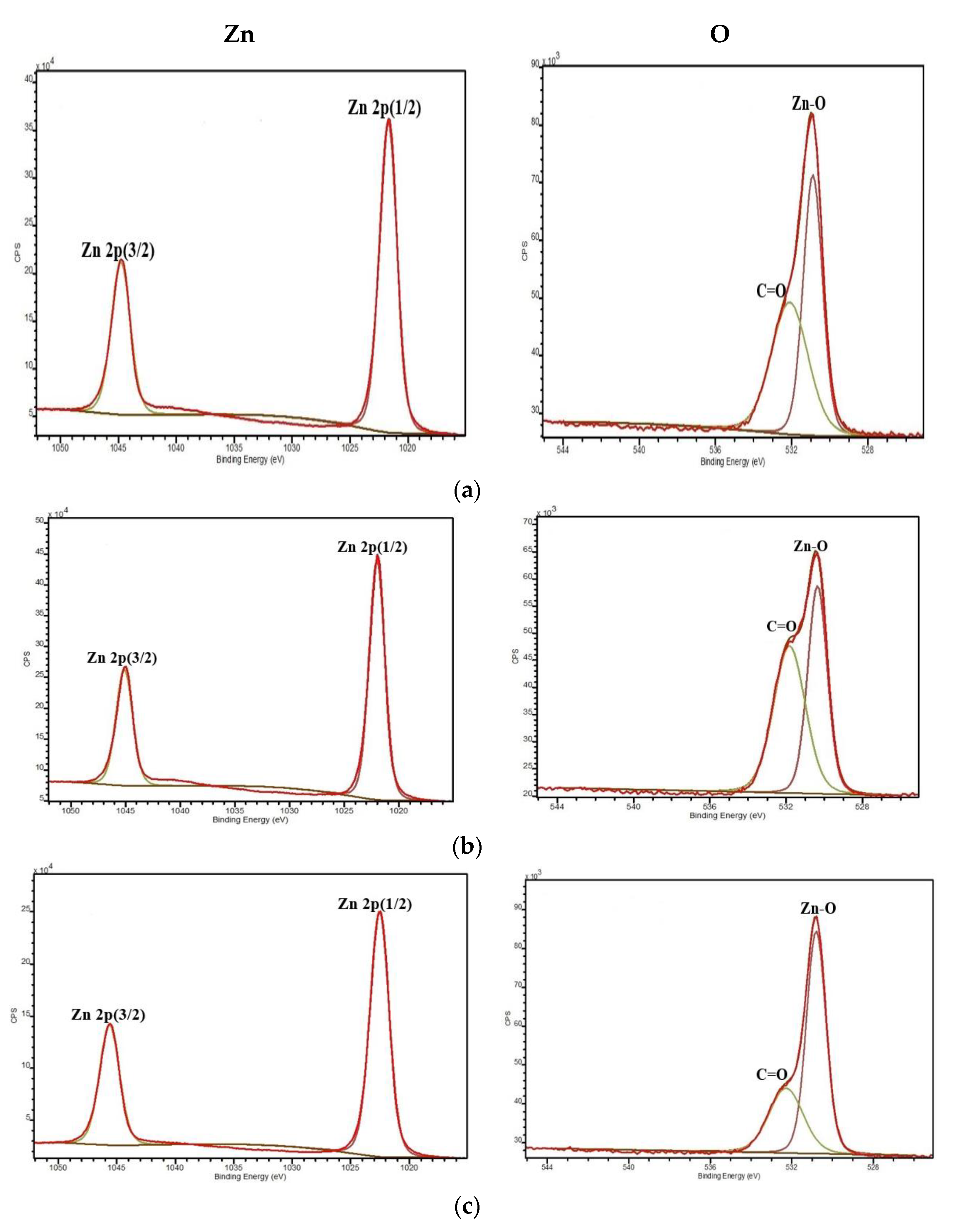
3.1. Chemical Composition Analysis

The chemical composition and the valence states of the zinc and oxygen species of the ZnO films (samples (#a), (#b) and (#c)) were monitored by XPS. Figure 1a–c show the complete survey XPS spectra of the prepared ZnO films. The peaks that appear in the spectra are mainly attributed to O, Zn, and C. Carbon detected by the C(1s) core level peak comes from the widespread presence of carbon contamination at the sample surfaces.
The principal core levels of Zn and O can be seen in Figure 2a–c. From this figure, we can observe a shift of Zn and O peaks from sample (#a) to (#c) certainly due to an effect of substrate’s temperature and to oxidation degree. Zn(2p1/2) and Zn(2p3/2) peaks shift from 1044.8 to 1045.8 eV and from 1021.5 to 1022.5 eV respectively for the three samples. The oxygen peak (O1s) is composed of two distinct components: the first one detected at 530.5 eV is due to Zn-O bonds and attributed to the difference in the electronegativity of oxygen and zinc, where the O2− ions are surrounded by Zn2+, showing the formation of the ZnO phase. The other oxygen peak, which is less intense and positioned at 532 eV, is related to C=O bonds probably coming from CO2 molecules loosely bounded on the surface.

3.2. Structural and Morphological Investigation

3.2.1. XRD Characterization

Figure 3a–c show the XRD patterns. For a better resolution of XRD spectra, we plot the intensity in logarithmic scale. From the figure, we can observe nine diffraction planes detected at 2θ around 33°, 35°, 36°, 44°, 60°, 62°, 67°, 69°, and 75°. According to the JCPDS card [40], the orientations at 33, 35, 36, and 67 are characteristic of the polycrystalline hexagonal wurtzite phases of the ZnO structure and correspond to the planes (100), (002), (101), and 67° respectively; they evolve significantly upon substrate heating. The peaks recorded at 44°, 60°, and 62° are attributed to SiO2 formed probably at the interface ZnO/Si under the heating effect. The two last peaks positioned at 2θ = 69° and 75° are due to the planes (004) and (113) of silicon substrate according to JCPDS 00-027-1402. The intensity of the (201) diffraction peak becomes the strongest at 400 °C because of the thickness of the ZnO, which is weak compared to that of the silicon substrate, which is thick. The increase of the intensity of the diffraction plane (103) testifies to the crystallization improvement of ZnO under heating of the substrate.
As we can see from Figure 3c, ZnO films deposited at 400 °C show the lowest peaks, which indicate that 400 °C is the optimum deposition temperature for obtaining structured ZnO with a good crystalline quality.
The lattice parameters a, b, and c were determined from the XRD spectra. The hexagonal structure is defined by a = bc, and the interplanar spacing d is a function that depends on a, b, c and on the indexed diffraction peaks (hkl), as shown in the following relation:
1 d 2 = 4 3 ( h 2 + h k + k 2 a 2 ) + l 2 c 2
The interplanar spacing d can also be determined from the following Bragg’s law below:
2dsinθ = nλ
where d is the interplanar spacing, θ is the Bragg diffraction angle, n is the order of diffraction (usually n = 1), and λ is the X-ray wavelength.
By combining Equations (1) and (2) and applying them to most intense peaks, we easily calculate the a and c lattice parameters. These values are summarized in Table 2.
It can be observed that the parameter a agrees reasonably with those reported in the literature, while c diverges slightly. This observation can be explained by the oxygen behavior in the subsurface of the film during the growth process conducting to the formation of ZnOx nanocrystaline phases. By using the X-ray line broadening method, the average ZnO crystallite sizes of the three synthesized samples ((#a), (#b), and (#c)) were estimated from the Debye–Scherrer formula [44].
D = 0.9 λ β ( 2 θ ) cos θ
where λ is the X-ray wavelength, θ is the Bragg diffraction angle, and β is the broadening of the diffraction peak measured at half of its maximum intensity.
The amount of defects in the synthesized ZnO films defined as the length of dislocation lines per unit volume of the crystal and representing the dislocation density can be estimated by the use of the equation.
δ = 1 D 2
where D is the average ZnO crystallite size determined from Equation (3).
We applied Equations (3) and (4) to the intense diffraction peak (002) of the samples (#a), (#b), and (#c). The obtained values of D and δ are shown in Table 3.
From these values, we can observe the decrease of the average crystallite size with the increase in substrate temperature. The crystallinity of the sample heated at 400 °C is more improved than for the other films prepared at lower temperature. The values of dislocation density for samples (#a), (#b), and (#c) confirm the improvement in ZnO crystallinity as the substrate temperature increases. That implied that the ZnO film prepared at 400 °C has good crystalline qualities.

3.2.2. SEM Results

The samples’ morphological properties are as important as the structural ones. Figure 4a,b show SEM images taken at resolution of 100 nm and with 200 × 103 magnification for samples (#a) and (#c). The samples show a textured and rough surfaces presented by granular structures composed of grains spherical in shape and uniformly distributed, which are small for sample (#a) and bigger for (#c). It is clear that the substrate temperature acts on ZnO grains which agglomerate into larger entities, which is in agreement with XRD results. Figure 4c shows the SEM image taken at magnification of 250 × 103 for sample (#c), which highlights the clustering of the ZnO grains with an increase of their size at 400 °C.

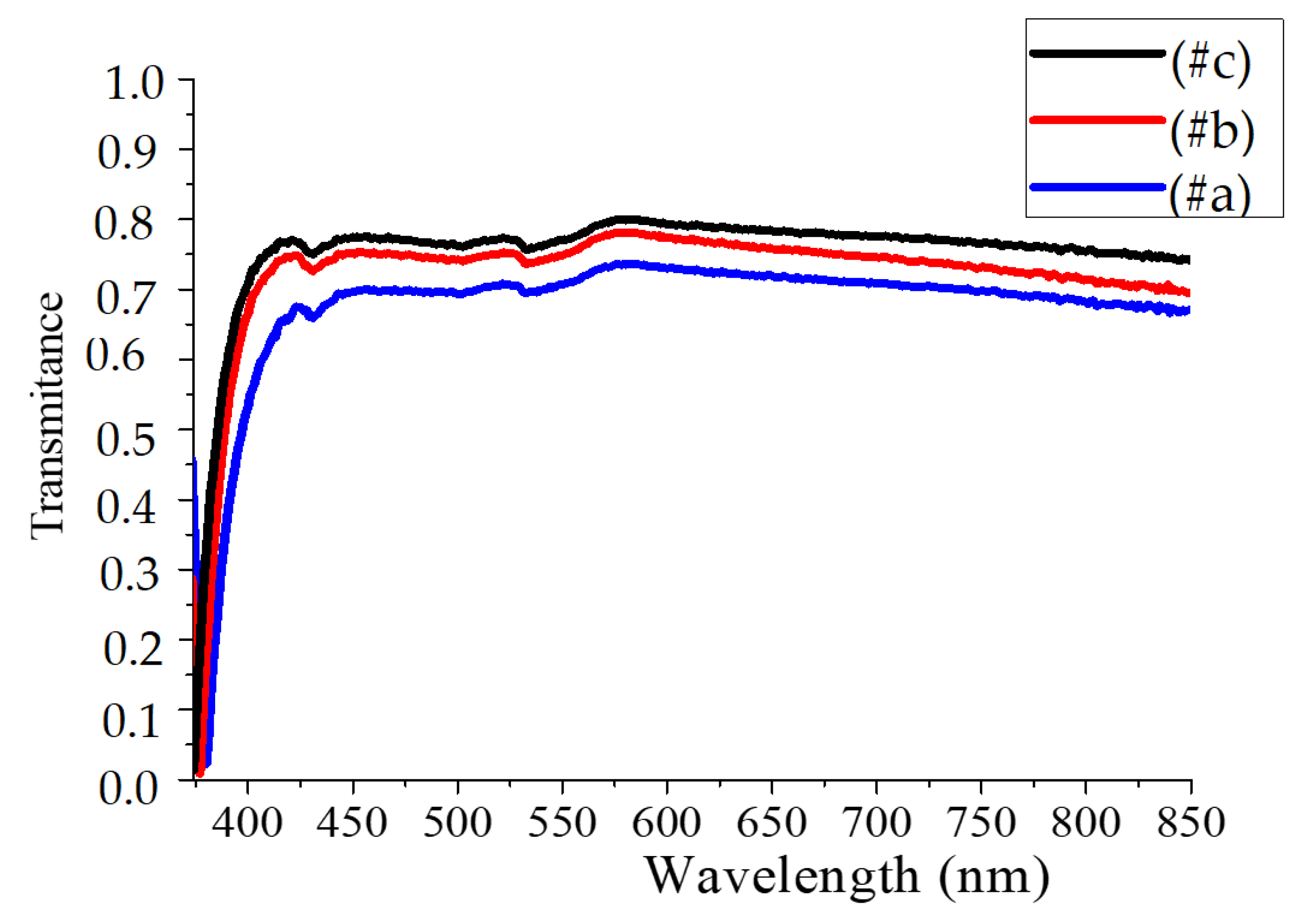
3.3. Optical Measurements

The optical properties of the ZnO thin films were studied with UV-visible spectroscopy using a double beam spectrophotometer in the wavelength range of 200–1000 nm. Figure 5 shows the transmittance spectra of the three samples ((#a), (#b), and (#c)). It may be observed that the transmittance yield of the samples (#a), (#b), and (#c) reaches a maximum of 70%, 75%, and 80% respectively. As we have discussed in previous paragraphs on the effect of substrate temperature, the ZnO films prepared on silicon heated to 400 °C are more transparent in the visible region compared to samples heated at 200 and 300 °C. By combining the data of the transmittance and absorption spectra, we can determine the value of the ZnO gap energy from the Tauc’s plot [45], using the equation below:
hν)2 = A(hν − Eg).
α is the absorption coefficient, hν is the photon energy, A is a constant and, Eg is the band-gap energy.
Figure 6 shows the Tauc plot where the value of the optical band gap is deduced from the intersection of the linear part on the hν energy axis. The values of Eg of samples (#a), (#b), and (#c) extracted from the linear extrapolation are reported in Table 4.
The values of the band gap obtained for our samples are in the range of some values reported in the literature [43,44,45,46]. Sample (#c) revealed a band-gap value of Eg = 3.3549 eV, which is close to the standard value of ZnO.

4. Conclusions

This paper studied the chemical composition, the structural, morphological, and optical properties of ZnO films deposited plasma-enhanced chemical vapor deposition. More particularly, the ZnO films were synthesized on silicon and glass substrates heated at 200, 300, and 400 °C. XPS characterization highlights the chemical composition of ZnO films, which are of good quality for the sample heated at 400 °C. XRD analysis showed polycrystalline phases of ZnO characterized by the hexagonal wurtzite structure with a high diffraction plane (002), which is the preferred growth orientation along this direction. The ZnO grain sizes determined from XRD spectra decreased with the increase of the substrate temperature. The crystallization of ZnO phases were improved at 400 °C, as confirmed by SEM images, which showed a coalescence of the ZnO nanograins with a size increase at 400 °C. UV-visible spectroscopy revealed a transmittance yield ranging between 70% and 80%, reaching 80% for the sample substrate heated at 400 °C. The optical band gap determined from Tauc plots indicated values in accordance with those of the literature. The determined transmittance yield and the band-gap energy values showed that our ZnO films synthesized by PECVD are of good transparency and semiconducting properties. The results are going to be tested for the fabrication of window coatings for light detection.

Author Contributions

M.G. proposed, designed the study and wrote the paper; N.H. and L.H. performed the experimental part and the processed of experimal spectra. M.A.D. contributed to the calculation of physical properties; A.B. treated XRD results; J.-J.P. revised the final manuscript’s english and discussed some results. In general all authors contributed to the discussion and interpretation of the results. All authors have read and agreed to the published version of the manuscript.

Funding

This research was funded by the Algerian Ministry of Education and Scientific Research (MESRS) in the framework of the PNE program.

Institutional Review Board Statement

Not applicable.

Informed Consent Statement

Not applicable.

Data Availability Statement

Data is contained within the article.

Acknowledgments

The authors thank the University of Chlef (Algeria) to have allowed to N. Hacini to benefit from the PNE Grant. M. Ghamnia would like to thank very much L. Houssiau for having welcomed the student N. Hacini at the LISE Laboratory of Namur University (Belgium) for carrying out this work.

Conflicts of Interest

The authors declare no conflict of interest.

References

  1. Choppali, U.; Kougianos, E.; Mohanty, S.P.; Gorman, B.P. Influence of annealing on polymeric precursor derived ZnO thinfilms on sapphire. Thin Solid Film. 2013, 545, 466–470. [Google Scholar] [CrossRef]
  2. Bedia, F.; Bedia, A.; Maloufi, N.; Aillerie, M.; Genty, F.; Benyoucef, B. Effect of tin doping on optical properties of nanostructured ZnO thin films grown by spray pyrolysis technique. J. Alloys Compd. 2014, 616, 312–318. [Google Scholar] [CrossRef]
  3. Hengehold, R.L.; Almassy, R.J.; Pedrotti, F.L. Electron energy loss and ultraviolet reflectivity spectra of crystalline ZnO. Phys. Rev. B 1970, 1, 4784–4791. [Google Scholar] [CrossRef]
  4. Gupta, T.K. Application of zinc oxide varistors. J. Am. Ceram. Soc. 1990, 73, 1817–1840. [Google Scholar] [CrossRef]
  5. Zeng, G.Y.; Nian, K.S.; Lee, K.Y. Characteristics of a dye-sensitized solar cell based on an anode combining ZnO nanostructures with vertically aligned carbon nanotubes. Diam. Relat. Mater. 2010, 19, 1457–1460. [Google Scholar] [CrossRef]
  6. Hassan, N.K.; Hashim, M.R. Structural and optical properties of ZnO thin film prepared by oxidation of Zn metal powders. In Proceedings of the 2012 International Conference on Enabling Science and Nanotechnology, Johor Bahru, Malaysia, 5–7 January 2012; Volume 42, pp. 1–2. [Google Scholar] [CrossRef]
  7. Saito, N.; Haneda, H.; Sekiguchi, T.; Ohashi, N.; Sakaguchi, I.; Koumoto, K. low-temperature fabrication of light-emitting zinc oxide micropatterns using self-assembled monolayers. Adv. Mater. 2002, 14, 418–421. [Google Scholar] [CrossRef]
  8. Chen, Y.; Bagnall, D.M.; Koh, H.-J.; Park, K.-T.; Hiraga, K.; Zhu, Z.; Yao, T. Plasma assisted molecular beam epitaxy of ZnO on c-plane sapphire: Growth and characterization. J. Appl. Phys. 1998, 84, 3912–3918. [Google Scholar] [CrossRef]
  9. Hvam, J.M. Temperature-induced wavelength shift of electron-beam-pumped lasers from CdSe, CdS and ZnO. Phys. Rev. B 1971, 4, 4459–4464. [Google Scholar] [CrossRef] [Green Version]
  10. Wang, L.-H.; Liang, J.; Ma, S.-F.; Liu, X.-G. Synthesis and characterization of the GaN film. Chin. J. Lumin 2008, 29, 152–155. [Google Scholar]
  11. Choudhary, S.; Gangopadhyay, S. Zincoxidenano-structures:Fromnano-walltonano-rodgrowthmorphology. AIP Conf. Proc. 2018, 1989, 020007–020012. [Google Scholar]
  12. Guileen, C.; Herrero, J. Structure, optical and electrical properties of indium tin oxide thin films prepared by sputtering at room temperature and annealed in air or nitrogen. J. Appl. Phys. 2007, 101, 073514–073521. [Google Scholar] [CrossRef]
  13. Chen, M.; Pei, Z.; Sun, C.; Wen, L.; Wang, X. Surface characterization of transparent conductive oxide Al-doped ZnO films. J. Cryst. Growth 2000, 220, 254–262. [Google Scholar] [CrossRef]
  14. Grundmann, M.; Rahm, A.; Nobis, N.; Lorenz, M.; Czekalla, C.; Evgeni, M.K.; Lenzner, J.; Boukos, N.; Travlos, A.; HeniniIn, M. Handbook of Self Assembled Semiconductor Nanostructures for Novel Devices in Photonics and Electronics; Elsevier: Amsterdam, The Netherlands, 2008; pp. 293–319. [Google Scholar]
  15. Ezema, F.I.; Nwankwo, U.O.A. Effect of annealing temperature on the structural and optical propertises of Al-doped zinc oxide (ZnO) crystals. J. Optoelectron. Biomed. Mat. 2010, 1, 167–173. [Google Scholar]
  16. Kluth, O.; Loffl, A.; Wieder, S.; Beneking, C.; Appenzeller, W.; Houben, L.; Rech, B.; Wagner, H.; Hoffmann, S.; Waser, R. Texture etched Al-doped ZnO: A new material for enhanced light trapping in thin film solar cells. In Proceedings of the Twenty Sixth IEEE Photovoltaic Specialists Conference—1997, Anaheim, CA, USA, 30 September–3 October 1997; pp. 715–718. [Google Scholar]
  17. Groenen, R.; Löffler, J.; Sommeling, P.; Linden, J.; Hamers, E.; Schropp, R.E.I.; VanDe Sanden, M. Surface textured ZnO films for thin film solar cell applications by expanding thermal plasma CVD. Thin Solid Film. 2001, 392, 226–230. [Google Scholar] [CrossRef]
  18. Löffler, J.; Groenen, R.; Linden, J.L.; Van de Sanden, M.C.M.; Schropp, R.E.I. Amorphous silicon solar cells on natively textured ZnO grown by PECVD. Thin Solid Film. 2001, 392, 315–319. [Google Scholar]
  19. Ouhaibi, A.; Ghamnia, M.; Dahamni, M.A.; Heresanu, V.; Fauquet, C.; Tonneau, D. The effect of strontium doping on structural and morphological properties of ZnO nanofilms synthesized by ultrasonic spray pyrolysis method. J. Sci. Adv. Mater. Devices 2018, 3, 29–36. [Google Scholar] [CrossRef]
  20. Hamzaoui, N.; Boukhachem, A.; Ghamnia, M.; Fauquet, C. Investigation of some physical properties of ZnO nanofilms synthesized by micro-droplet technique. Results Phys. 2017, 7, 1950–1958. [Google Scholar] [CrossRef]
  21. Bekhti, W.; Ghamnia, M.; Guerbous, L. Effect of some amines, dodecylamine (DDA) and hexadecyldimethylamine (DMHA), on the formation of ZnO nanorods synthesized by hydrothermal route. Philos. Mag. 2014, 94, 2886–2899. [Google Scholar] [CrossRef]
  22. Matsuo, T.; Okuda, S.; Washio, K. Growth and characterization of ZnO thin film by RF magnetron sputtering for photoacoustic tomography sensor. MRS Online Proc. Libr. Arch. 2013, 1494, 19–24. [Google Scholar] [CrossRef]
  23. Srinivasarao, K.; Srinivasarao, G.; Madhuri, K.V.; Murthy, K.K.; Mukhopadhyay, P.K. Preparation and characterization of RF magnetron sputtered Mo:ZnO. Thin Films Indian J. Mat. Sci. 2013, 2013, 1–7. [Google Scholar]
  24. Al Asmar, R.; Zaouk, D.; Bahouth, P.; Podleki, J.; Foucaran, A. Characterization of electron beam evaporated ZnO thin films and stacking ZnO fabricated by e-beam evaporation and RF magnetron sputtering for the realization of resonators. Microelectron. Eng. 2006, 83, 393–398. [Google Scholar] [CrossRef]
  25. Agarwal, D.C.; Chauhan, R.; Kumar, A.; Kabiraj, D.; Singh, F. Synthesis and characterization of ZnO thin film grown by electron beam evaporation. J. Appl. Phys. 2006, 99, 123105. [Google Scholar] [CrossRef]
  26. Vincze, A.; Bruncko, J.; Michalka, M.; Figura, D. Growth and characterization of pulsed laser deposited ZnO thin films. Open Phys. 2007, 5, 385–397. [Google Scholar] [CrossRef] [Green Version]
  27. Wisz, G.; Virt, I.; Sagan, P.; Potera, P.; Yavorskyi, R. Structural, optical and electrical properties of Zinc oxide layers produced by pulsed laser deposition method. Nanoscale Res. Lett. 2017, 12, 253. [Google Scholar] [CrossRef] [Green Version]
  28. Asghar, M.; Mahmood, K.; Raja, M.Y.; Hasan, M. Synthesis and characterization of ZnO nanorods using molecular beam epitaxy. Adv. Mat. Res. 2013, 622, 919–924. [Google Scholar] [CrossRef]
  29. Zhou, Y.; Yu, G.; Shi, X.; Zhang, X.; Yan, W.; Wei, S.; Xie, Y. Growth and characterization of ZnO thin film prepared by molecular beam epitaxy on Si(100). Nucl. Tech. 2003, 26, 9–12. [Google Scholar]
  30. Ilican, S.; Caglar, Y.Y.; Caglar, M. Preparation and characterization of ZnO thin films deposited by sol-gel spin coating method. J. Optoelectr. Adv. Mat. 2008, 10, 2578–2583. [Google Scholar]
  31. Firdaus, C.; Rizam, M.; Rusop, M.; Hidayah, S. Characterization of ZnO and ZnO: TiO2 thin films prepared by sol-gel spray-spin coating technique. Procedia Eng. 2012, 41, 1367–1373. [Google Scholar] [CrossRef]
  32. Cruz, M.R.A.; Zarzosa, G.O.; Castañón, G.M.; Martinez, J.R. Characterization of ZnO threads obtained using dipcoatingmethod at room temperature. Mat. Lett. 2012, 78, 159–161. [Google Scholar] [CrossRef]
  33. Rani, R.A.; Ab Ghafar, S.; Zoolfakar, A.S.; Rusop, M. Growth of ZnO nanorods on glass substrate deposited using dipcoatingmethod. Nanosci. Nanotechnol. Nano-Scitech 2018, 1963, 02007. [Google Scholar] [CrossRef]
  34. Ergin, B.; Ketenci, E.; Atay, F. Characterization of ZnO films obtained by ultrasonic spray pyrolysis technique. Int. J. Hydrog. Energy 2009, 34, 5249–5254. [Google Scholar] [CrossRef]
  35. Alver, U.; Solakyildirim, T.K.; Bacaksız, E.; Kucukomeroglu, T.; Nezir, S.; Mutlu, I.H.; Aslan, F. Synthesis and characterization of spray pyrolysis zinc oxide microrods. Thin Sol. Film. 2007, 515, 3448–3451. [Google Scholar] [CrossRef]
  36. Chen, Z.; Salagaj, K.S.; Strob, W.Z.K. ZnO thin films synthesized by chemical vapor deposition. In Proceedings of the 2010 IEEE Long Island Systems, Applications and Technology Conference, Farmingdale, NY, USA, 7 May 2010. [Google Scholar]
  37. Reuge, N.; Bacsa, R.R.; Serp, P.; Caussat, B. Chemical vapor synthesis of zinc oxide nanoparticles: Experimental and preliminary modeling studies. J. Phys. Chem. C 2009, 113, 19845–19852. [Google Scholar] [CrossRef]
  38. Salar, E.; Ghoranneviss, M. Growth and characterization of carbon nanotubes and zinc oxide nanocomposite with the PECVD technique. Results Phys. 2017, 7, 1006–1009. [Google Scholar] [CrossRef]
  39. Chao, H.; Wei, D.H. Synthesis and Characterization of high c-axis ZnO thin film by plasma enhanced chemical vapor deposition, system and its UV photodetector application. J. Vis. Exp. 2015, 104, e53097. [Google Scholar] [CrossRef] [PubMed] [Green Version]
  40. Vimalkumar, T.; Poornima, N.; Kartha, C.S.; Vijayakumar, K. On tuning the orientation of grains of spray pyrolysed ZnO thin films. Appl. Surf. Sci. 2010, 256, 6025–6028. [Google Scholar] [CrossRef] [Green Version]
  41. Khoshhesab, Z.M.; Sarfaraz, M.; Asadabad, M.A. Preparation of ZnO nanostructures by chemical precipitation method. Synth. React. Inorg. Met. Chem. 2011, 41, 814–819. [Google Scholar] [CrossRef]
  42. Bindu, P.; Thomas, S. Estimation of lattice strain in ZnO nanoparticles: X-ray peak profile analysis. J. Appl. Phys. 2014, 8, 123–134. [Google Scholar] [CrossRef] [Green Version]
  43. Marouf, S.; Beniaiche, A.; Guessas, H.; Azizi, A. Morphological, structural and optical properties of ZnO thin films deposited by dip coating method. Mater. Res. 2016, 20, 88–95. [Google Scholar] [CrossRef] [Green Version]
  44. Cullity, B.D.; Weymouth, J.W. Elements of X-Ray Diffraction. Am. J. Phys. 1957, 25, 394–395. [Google Scholar] [CrossRef] [Green Version]
  45. Tauc, J.; Menth, A. States in the gap. J. Non-Cryst. Solids 1972, 8, 569–585. [Google Scholar] [CrossRef]
  46. Shinde, S.; Oh, Y.; Haranath, D.; Bhosale, C.; Rajpure, K.; Shinde, P.S. Structural, optoelectronic, luminescence and thermalproperties of Ga-doped zinc oxide thin films. Appl. Surf. Sci. 2012, 258, 9969–9976. [Google Scholar] [CrossRef]
  47. Wang, Z.L. Zinc oxide nanostructures: Growth, properties and applications. J. Phys. Condens. Matter 2004, 16, R829–R858. [Google Scholar] [CrossRef]
  48. Zargar, R.A.; Hassan, M.M.; Boora, N.; Ahmed, I.; Ahmed, S.; Nissa, K.H.; Kumari, S.; Hafiz, A.K. A comparative study of microand nano ZnO films fabricated by sol-gel syringe spray method. Int. J. Ceram. Eng. Sci. 2020, 2, 169–176. [Google Scholar] [CrossRef]
  49. Khan, M.; Bhatti, K.; Qindeel, R.; Alonizan, N.; Althobaiti, H.S. Characterizations of multilayer ZnO thin films deposited bysol-gel spin coating technique. Results Phys. 2017, 7, 651–655. [Google Scholar] [CrossRef]
Figure 1. XPS spectra of the ZnO films synthesized on silicon substrate: (a) substrate heated at 200 °C, (b) substrate heated at 300 °C, (c) substrate heated at 400 °C.
Coatings 11 00202 g001
Figure 2. The principal XPS core levels of Zn and O. (a): substrate heated at 200 °C, (b): substrate heated at 300 °C, (c): substrate heated at 400 °C.
Coatings 11 00202 g002
Figure 3. XRD spectra of the ZnO films synthesized by the PECVD method. (a): substrate heated at 200 °C, (b): substrate heated at 300 °C, (c): substrate heated at 400 °C.
Coatings 11 00202 g003
Figure 4. SEM images for samples (#a) and (#c) of ZnO films synthesized on silicon substrates: (a) heated at 200, (b) heated at 400 °C, (c) SEM image taken at magnification of 250 × 103 of sample heated at 400 °C.
Coatings 11 00202 g004
Figure 5. Transmittance spectra of the ZnO films synthesized on glass substrates (a): ZnO/glass substrate heated at 200 °C, (b): ZnO/glass substrate heated at 300°C, (c): ZnO/glass substrate heated at 400 °C.
Coatings 11 00202 g005
Figure 6. Plot of (αhν) vs. hν and determination of the band-gap energy (Eg): (a) ZnO/glass substrate heated at 200 °C, (b) ZnO/glass substrate heated at 300 °C, (c) ZnO/glass substrate heated at 400 °C.
Coatings 11 00202 g006
Table 1. Codes for the different ZnO films prepared by the plasma-enhanced chemical vapor deposition (PECVD) technique on Si(001) substrates heated at 200, 300, and 400 °C during film deposition
SamplesTemperature (°C)
(#a)200
(#b)300
(#c)400
Table 2. Values of the a and c crystalline parameters determined from the XRD spectra treatment.
Sample2θ(hkl)d (Å)a (Å)a (Å) in Literaturec (Å)c (Å) in Literature
(#a)34.9
36.0
(0 0 2)
(1 0 1)
2.5989
2.4801
3.25863.2400 [41]5.19795.2100 [41]
(#b)35.0
36.5
(0 0 2)
(1 0 1)
2.6055
2.4758
3.24893.2229 [42]5.21095.1755 [42]
(#c)34.9
36.0
(0 0 2)
(1 0 1)
2.5989
2.4801
3.25862.9950 [43]5.19795.1890 [43]
Table 3. Determination of the ZnO grain size and defect density by the use of the Debye–Scherrer relation.
Sample2θ (°)β (°)D (nm)δ (10−4·nm−2)
(#a)34.90.234272.181.919
(#b)35.00.290058.132.959
(#c)34.90.535331.579.960
Table 4. Determination of Eg band-gap values from the plot of (αhν) vs. hν and comparison to literature data.
SampleCalculated Eg (eV)Eg (eV) in Literature
(#a)3.28683.37 [46]
3.4, 3.34 [47,48]
(#b)3.31703.72–3.85 [49]
(#c)3.3549
Publisher’s Note: MDPI stays neutral with regard to jurisdictional claims in published maps and institutional affiliations.

