Article

Theoretical and Experimental Analysis of Surface Roughness and Adhesion Forces of MEMS Surfaces Using a Novel Method for Making a Compound Sputtering Target

1
Department of Mechanical Engineering, Najafabad Branch, Islamic Azad University, Najafabad 8514143131, Iran
2
School of Engineering, Macquarie University, Sydney, NSW 2109, Australia
3
National Institute for Research & Development in Chemistry and Petrochemistry—ICECHIM, Splaiul Independentei no. 202, 6th District, 060021 Bucharest, Romania
4
Faculty of Applied Chemistry and Materials Science, Department of Inorganic Chemistry, Physical Chemistry and Electrochemistry, University Politehnica of Bucharest, Ghe. Polizu Street, no. 1-7, 011061 Bucharest, Romania
*
Author to whom correspondence should be addressed.
Coatings 2021, 11(12), 1551; https://doi.org/10.3390/coatings11121551
Submission received: 1 November 2021 / Revised: 29 November 2021 / Accepted: 15 December 2021 / Published: 17 December 2021
(This article belongs to the Special Issue Novel Approaches to Hybrid Films or Coatings)

Abstract

:
Achieving a compound thin film with uniform thickness and high purity has always been a challenge in the applications concerning micro electro mechanical systems (MEMS). Controlling the adhesion force in micro/nanoscale is also critical. In the present study, a novel method for making a sputtering compound target is proposed for coating Ag–Au thin films with thicknesses of 120 and 500 nm on silicon substrates. The surface topography and adhesion forces of the samples were obtained using atomic force microscope (AFM). Rabinovich and Rumpf models were utilized to measure the adhesion force and compare the results with the obtained experimental values. It was found that the layer with a thickness of 500 nm has a lower adhesion force than the one with 120 nm thickness. The results further indicated that due to surface asperity radius, the adhesion achieved from the Rabinovich model was closer to the experimental values. This novel method for making a compound sputtering target has led to a lower adhesion force which can be useful for coating microgripper surfaces.

1. Introduction

Since miniaturization provides unique advantages such as reduced energy consumption, more effective portability, occupying less space, and improved performance, many industries have welcomed it. This phenomenon has emerged in many applications, including the electronics, automotive, military, and medical industries. Simultaneous miniaturization of electronic and mechanical devices by utilizing microfabrication techniques has led to the creation of microelectromechanical systems (MEMS) [1,2,3,4]. Silicon, meanwhile, has excellent electrical and mechanical properties, making it an appropriate material for MEMS devices [5,6,7]. The development of micromanipulation systems, which occurred due to further miniaturization of components, resulted in the design of microgrippers [8,9]. Manipulation of micro- and nano-scale objects with precise control and without causing destruction has become a critical issue in nanotechnology fields [10,11,12]. Given the high surface-to-volume ratio of MEMS, the adhesive forces might exceed the elastic restoring force. Then, the contact parts and components stick to each other and make the entire system inoperative [13,14]. Therefore, adhesion can be mentioned as one of the most important challenges in MEMS as well as microgrippers. One solution to carefully monitor the adhesion force considerably is creating rough surfaces made out of, or coated with, hard or hydrophobic materials [15,16,17]. There are two prevalent deposition techniques to coat thin films on a surface, namely, physical and chemical depositions. The magnetron sputtering method, a kind of physical deposition technique, is more welcome than other methods since a vast range of materials with high purity, uniform thickness and good film-forming can be created on the surface [18]. Behera et al. [19] investigated the adhesion condition of BCP-TiO2 composite films deposited by magnetron sputtering before and after the addition of TiO2. They deposited the composite thin films on Ti-6Al-4V substrates and analyzed surface morphology and adhesion behavior. Their results indicated that the adhesion strength and surface roughness rose after the addition of TiO2. In other research, Barajas-Valdes et al. [20] examined the nanomechanical properties, including adhesion, of pure aluminum and aluminum-boron thin films manufactured by magnetron sputtering. They deposited the thin films on glass substrates and silicon wafers. The use of characterization techniques led to the fact that film’s mechanical behavior can be influenced by material target, substrate type, and sputtering conditions. It was found that composite films have greater adhesion than pure aluminum films. An atomic force microscope (AFM) is commonly used for determining the adhesion force [21,22,23]. In this regard, Johnson–Kendall–Roberts (JKR), Derjaguin–Muller–Toporov (DMT) and Hertzian theory (HERTZ), which are theoretical models, are regularly used [24,25,26]. Rabinovich et al. [27] considered contact mechanics theory to measure the interaction force. They presented a physical model in which both the radius and the height of the asperities are utilized to calculate the adhesion force. Consequently, this model is more reliable with a nano-scale roughness than other models for measuring the adhesion between the particle and surface. Another theoretical model which is used for calculating the adhesion force is Rumpf. This model is utilized for particle adhesion to the surface, maintaining submicroscopic roughness [28,29]. Unlike the Rumph model, Rabinovich uses the radius of the asperities.
The usage of composite thin films has invariably been of interest to researchers in various applications, such as integrated circuits (IC), sensors and microgrippers. Magnetron sputtering has been proposed as a practical method for depositing composite thin films on MEMS surfaces.
Buranich et al. [30] analyzed the microstructure, mechanical, and tribological properties of HfB2 deposited from the compound target. The deposition process was done by means of magnetron sputtering, and the films were deposited on stainless-steel substrates. They employed nanoindentation, tribology (balloon-disk), and nano-scratch (friction) to inspect the compound layers. They discovered that the most notable dependence of features on microstructure could be seen in films with a thickness of 1–2 μm. The examination of AlN thin films to find the optimal target sputtering mode was conducted by Ma et al. [31]. Deposition of the layers was performed using magnetron sputtering, and the formation of crystals, residual stress, surface roughness, and morphology of AlN thin films were considered by studying the impact of aluminum target sputtering mode and sputtering power. They concluded that lower surface roughness and residual stress could be obtained by transitional mode. Also, when the sputtering power increases in transitional mode, the residual stress becomes smaller.
Since making composite targets is not only expensive but also time-consuming, researchers use several targets or co-sputtering methods to create a composite surface. In this way, the targets are placed parallel or at an angle to the substrate [32,33,34].
Mertin et al. [35] considered the durability and reliability of optical coatings using magnetron co-sputtering. The targets from magnesium fluoride (MgF2) and fused silica were chosen to coat nano-composite Mg–F–Si–O films. The installation of targets was at an angle of 90° to each other, confronting the static substrate at 45° to create a parallel gradient in the thin-film fabrication. This change in the targets’ placement angles led to films consisting of MgF2 nanocrystals embedded in a SiO2-rich amorphous matrix. In another investigation, Mazur et al. [36] studied the structure of Ti–Cu thin films employing magnetron sputtering with separate Cu and Ti targets. Three various profiles of powering the magnetron were applied to analyze the elements’ gradient distribution. It was found that structural changes alternated with the amount of Ti and Cu in specific regions of deposited coatings.
This study presents a novel method for making a sputtering compound target and then investigates the impact of this deposition on adhesion force and surface roughness. In this study, single layers of Ag and Au with 120 and 500 nm thickness and an Ag–Au compound layer with analogous thicknesses were produced for microgrippers on silicon substrates. Afterward, the surface topographies were obtained using AFM. Eventually, the experimental data of surface topographies, theoretical models of Rabinovich and Rumpf, and the surface forces results taken from each coating and thickness were assessed and compared.

2. Materials and Methods

Silver and gold single layers and Ag–Au compound layers were coated on the silicon substrate (Si <100>). The magnetron sputtering method was selected to coat layers as a wide array of materials can be deposited by this method, and the produced films have suitable uniformity and compactness. A novel method for manufacturing a sputtering target was proposed in this study to achieve a compound thin film with 120 and 500 nm thicknesses. Finally, the AFM microscope (JPK company, Berlin, Germany), Rabinovich, and Rumpf models were used to investigate the impact of this compound thin film on adhesion forces and surface roughness and compare the results with Ag and Au single layers.

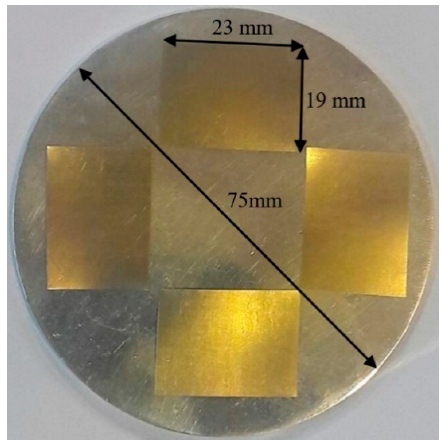
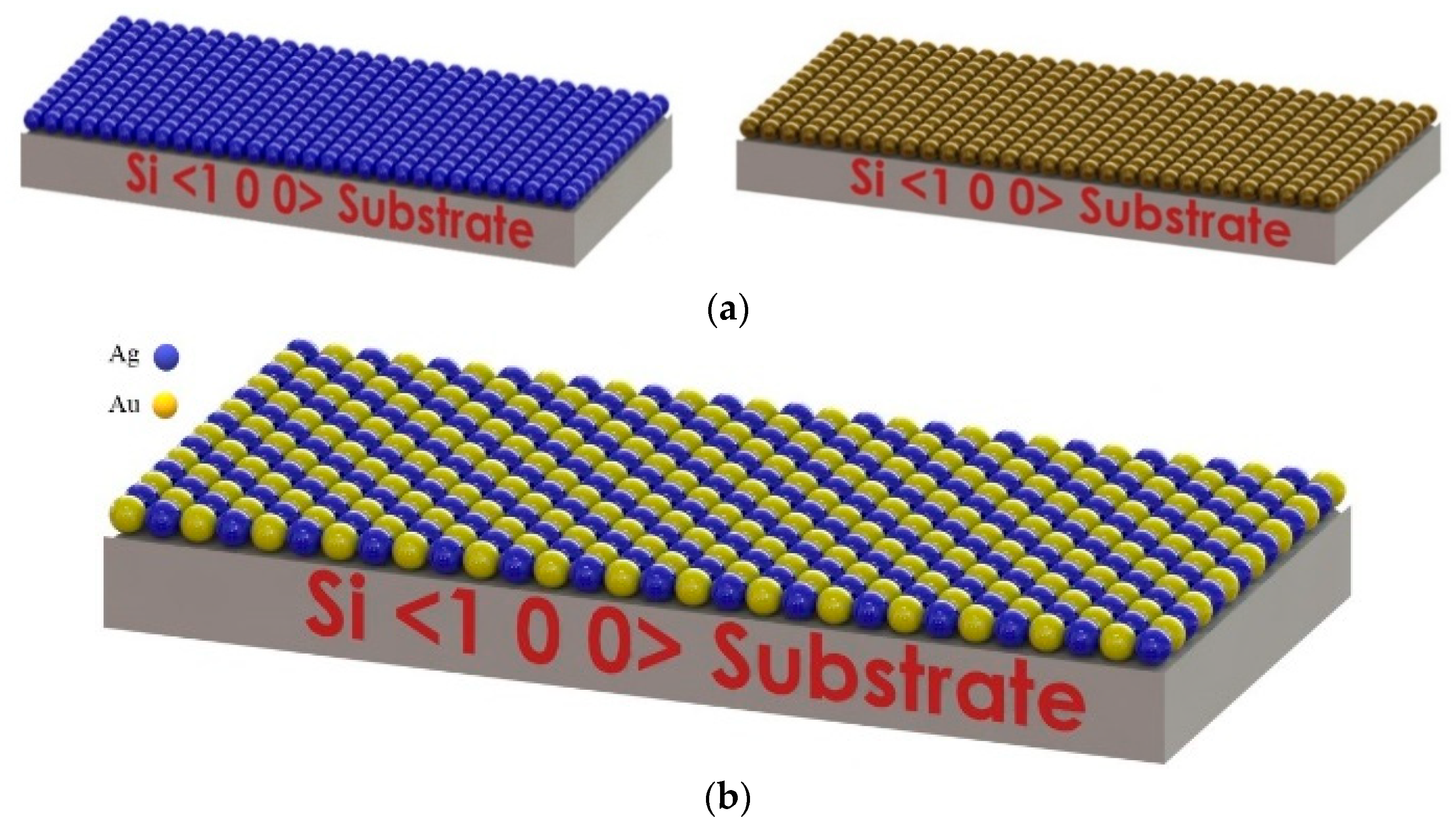
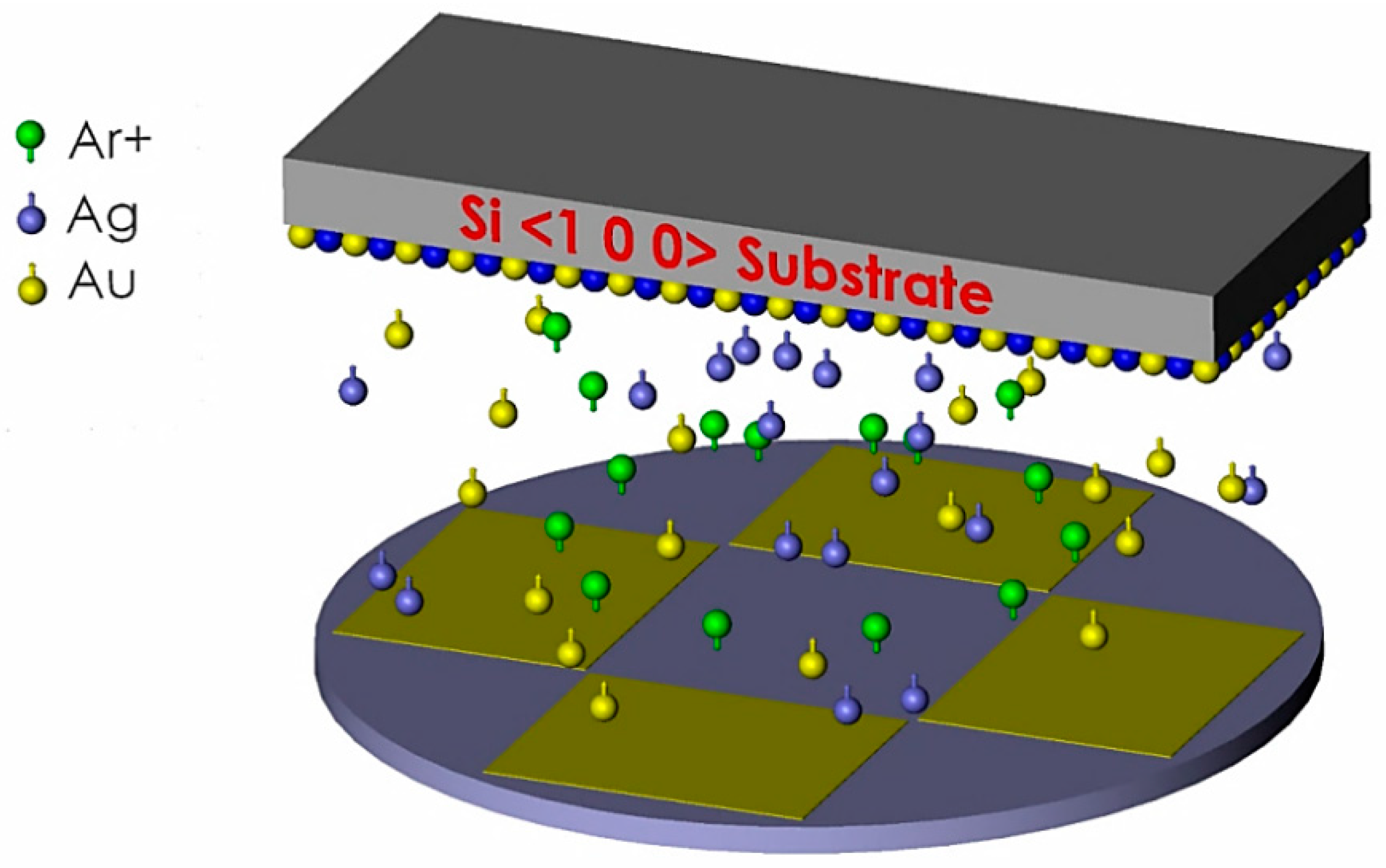
2.1. Manufacturing of Ag–Au Compound Target

The targets of the magnetron sputtering method are in the form of a disk, typically with 2 to 5 mm thickness. Some methods such as cutting a disk from a pure material and casting are employed to make the target. Ag and Au were selected for manufacturing the target for this study. Gold is frequently used in microsystems due to its high electrical and thermal conductivity and excellent corrosion resistance [37,38]. Silver possesses antibacterial properties, which makes it an excellent choice for medical microgrippers [39,40].
Figure 1 demonstrates a magnetron sputtering target graphically. Owing to the magnetic field below the target, some target zones are most exposed to argon ions, depicted in red in the figure. The parts are shown in blue play the least role in the sputtering process. Since this paper aims to create a compound layer of gold and silver, the effective part of the target, which is shown in red, is paramount.
To make the Ag–Au target, first, the silver target with 99.99% purity was melted in the crucible, and then it was created in the form of a disk with a thickness of 3 mm and a diameter of 75 mm. Following on from this, the gold sheets with 99.99% purity were made by the rolling method with a thickness of 0.1 mm and placed on the silver disk (the red part in Figure 1). The equations and details for making this compound target are described below.
R1 and R2 are the radiuses of the blue and red zones, respectively. As explained, the red part in the target is effective in the coating process. Therefore, the area of the blue zone must be subtracted from the total target to determine the area of the red zone used in depositing the layers. Also, the outer blue edge is removed from the entire radius of the target and does not affect the formulas.
Equation (1) shows how the area of deposition (AD) is calculated:
A D = π ( R 2 2 R 1 2 )
At 600 voltage, the argon gas sputtering yield for Au and Ag is r A u = 2.43   and r A g = 3.40   respectively. The proportion of deposition ratio ( P D r ) of Ag to Au is:
P D r = r A g r A u
Thus, the total deposition ratio ( T D r ) is:
  T D r = 1 + P D r
The calculation of the area of the target surface covered with silver is as follows:
A D A g = A D T D r
This area is deducted from the entire surface of the target to measure the amount of gold area, which is to be located over the silver zone:
A D A u = A D A D A g
The placement of the gold films on the silver surface of the target must be symmetrically (Figure 2) due to the random strike of the target surface by argon ions. Therefore, 99.99% pure gold film with 23 × 19 mm2 dimensions was divided into four parts. The final Ag–Au target made for this study is presented in Figure 2.

2.2. The Coating Process

After preparing the targets, the magnetron sputtering device (Explorer, Denton Vacuum, NJ, USA) was employed to produce thin films with 120 and 500 nm thicknesses. For accurate control and measurement of thin films’ thickness, a quartz crystal was employed. Our deposition system was equipped with this device that measures a mass change per crystal area by measuring frequency change. Table 1 reveals the conditions under which the deposition process took place.
Figure 3 illustrates the magnetron sputtering process with the presence of this novel target schematically. Regarding this figure, when the chamber is vacuumed, the neutral argon gas enters the chamber, resulting in chamber electrical discharge, ionization of argon, and the creation of positive ions. These ions collide with the Ag–Au surface target and separate from it while the energy and momentum are transferred to the atoms. This process leaves the target with a particular amount of energy. Finally, the atom accumulation occurs on the silicon substrate, fabricating a compound thin film.
Figure 4 demonstrates the surfaces of this study after the coating process. Single layers of Ag and Au and compound layers of Ag–Au were utilized to investigate the effect of this novel target making in adhesion forces and surface roughness.

3. Results and Discussion

After the deposition process, the AFM Nano wizard II of JPK Company (Berlin, Germany) was applied to calculate the adhesion forces and perform surface imaging. The AFM cantilever (AppNano company, Mountain View, CA, USA) with a silicon tip in V shape, 0.292 N/m spring constant, 10 nm tip radius, and 66 kHz vibrational frequency was utilized.

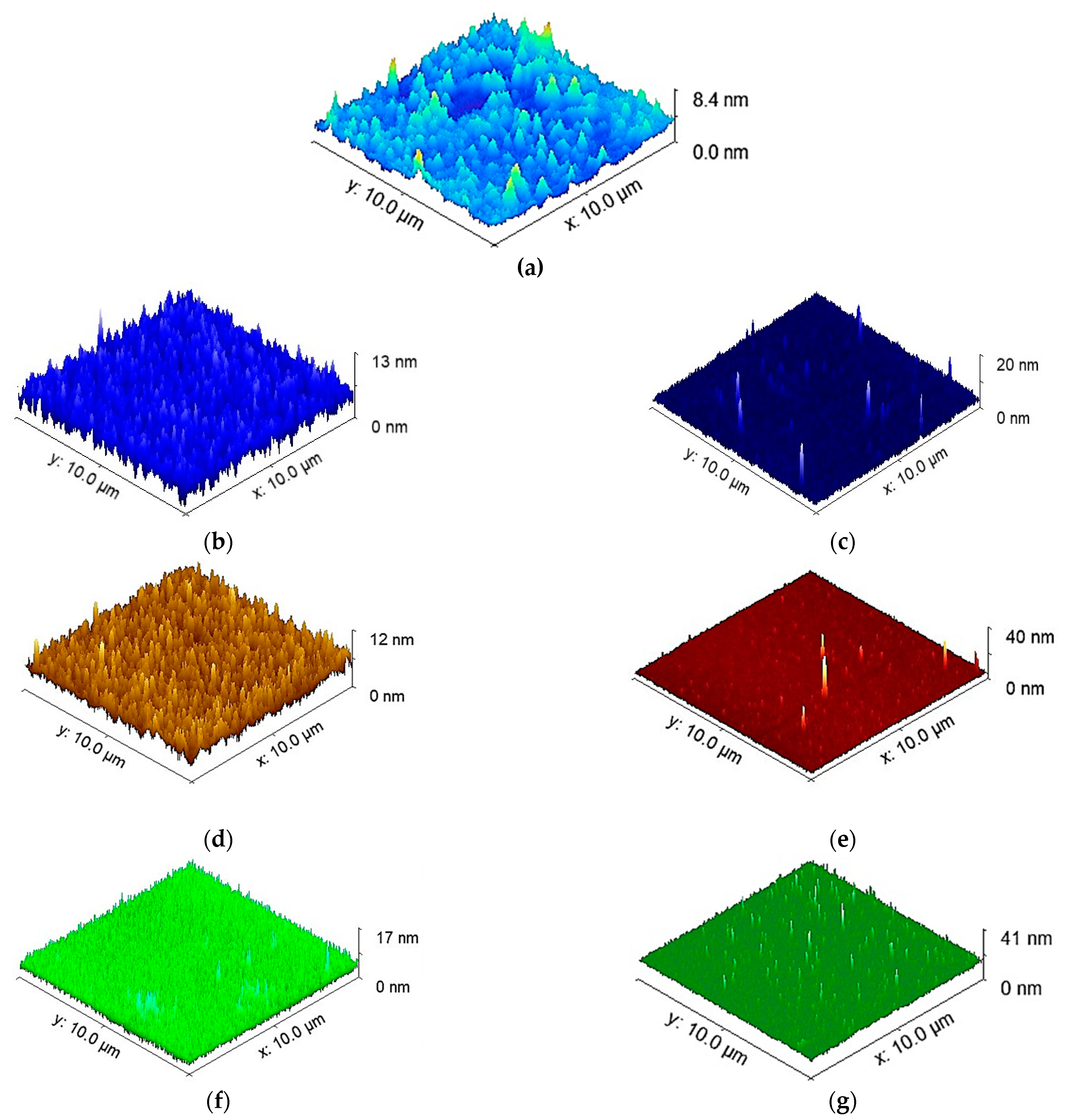
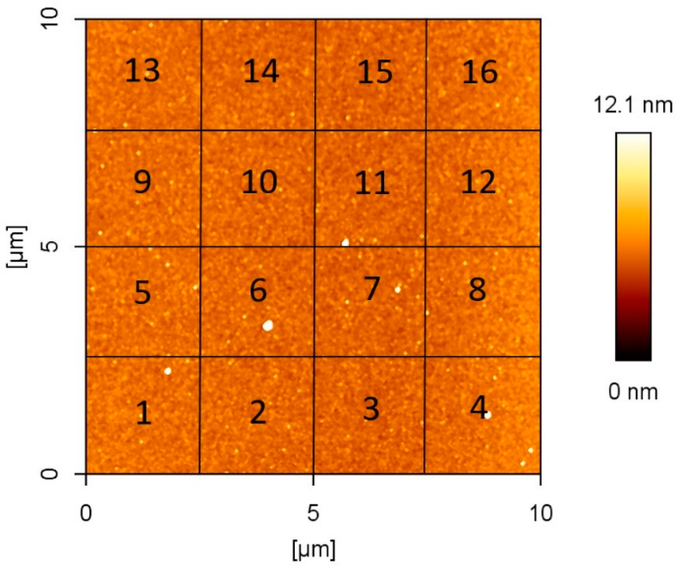
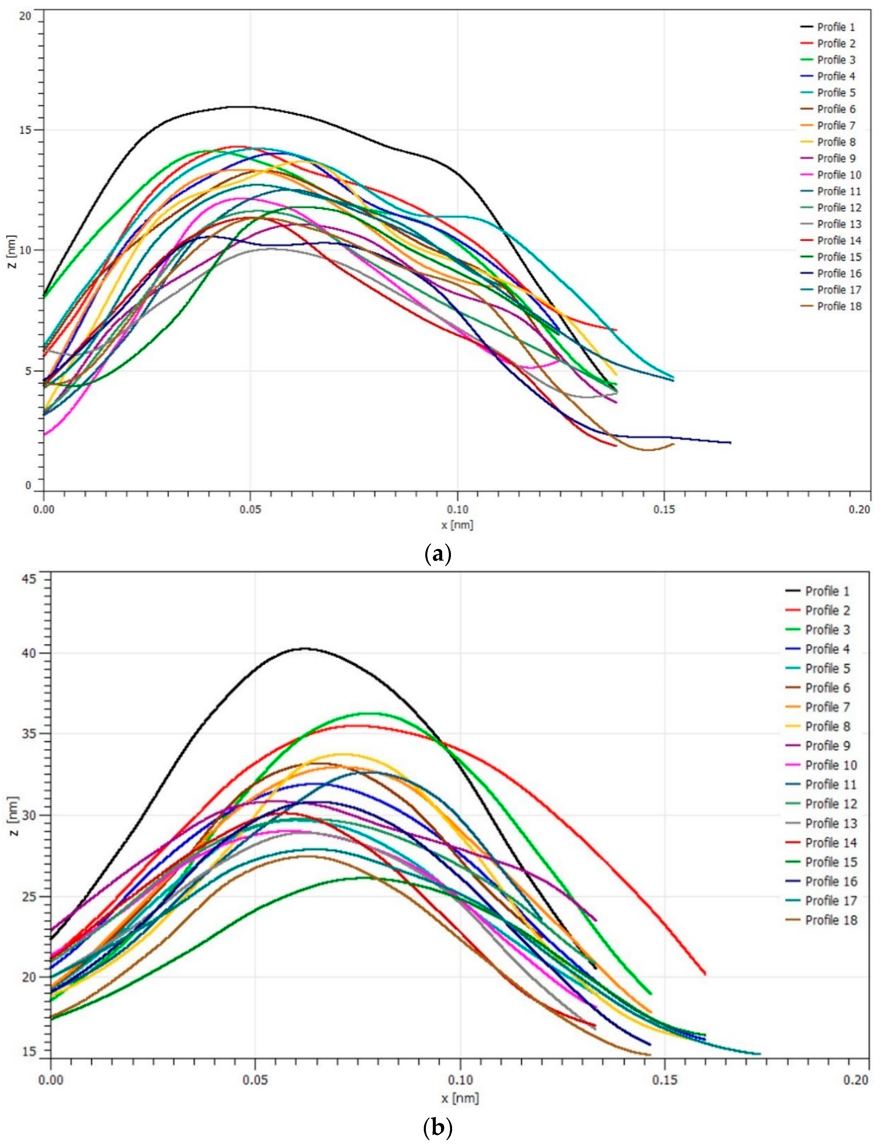
3.1. Surface Topography

The topography of the surfaces was analyzed to study the geometric properties of samples. In an ambient atmosphere and with 22 °C, temperature the AFM imaging was accomplished. Notice that all the samples have been rinsed with a solution before ascertaining the topography. To this end, water and soap were used to wash the substrates. Next, the substrates were rinsed with acetone, isopropanol, dichloromethane, ethanol, methanol, acetone, and deionized water. Eventually, to dry the substrates, nitrogen gas pressure was employed immediately. The features of the surfaces coated with single layers of silver and gold and compound layers of Ag–Au with thicknesses of 120 and 500 nm were considered by Gwyddion, as presented in Table 2 and Figure 5.
In order to calculate the parameters of Ra, Rms, and Ymax, from each sample, 18 images were taken from various areas of the surface. Then in each area, these parameters were measured, and finally, the average value of all 18 areas was presented in Table 2. The three-dimensional images of Figure 5 and the data presented in Table 2 show that surfaces with a 500 nm thickness coating have the highest asperities. The surfaces with a thickness of 500 nm demonstrate the maximum surface roughness (Ra). Furthermore, the parameters of Ra, root mean square (Rms), and height of asperities (Ymax) have the highest value for deposition thickness of 500 nm, which suggests that a rise in the deposition thickness results in more elevated surface roughness parameters. The uncoated silicon surface has the minimum roughness (Ra) and proves that the film deposition effectively increases surface roughness parameters.
According to Table 2, since Ra, Rms, and height of asperities (Ymax) parameters have risen by increasing thickness from 120 to 500 nm, it can be said that the accumulation of atoms on the surface after the coating process is one of the reasons for augmenting the number of asperities.

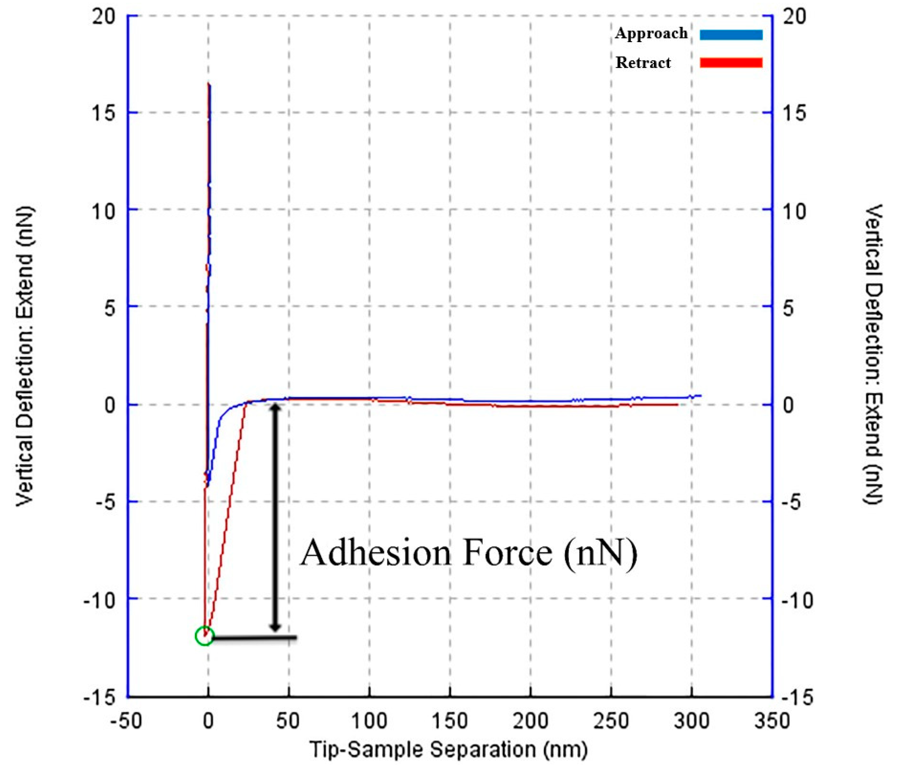
3.2. Experiemental Adhesion Force

Measuring the interaction force with an AFM can be accomplished by analyzing the movement of the cantilever tip on the surface. When the tip is separated from the surface, the forces between the tip and the sample cause deflection in the cantilever, and from here, it is viable to measure the adhesion force by considering this deflection. Figure 6 is the force–distance curve obtained from the AFM and (version 5.0.96) JPKSPM Data Processing software.
While the vertical axis depicts the applied force to the tip, the horizontal axis represents the tip displacement. The tip jumps toward the surface when it approaches the surface. This phenomenon happens due to the existence of Van der Waals, the electrostatic and capillary forces, known as adhesion forces [32]. The double arrow from the zero line represents the adhesion force. To increase the reliability of the calculated adhesive force, the measurements were made at several points. A grid of 16 squares was considered for each sample (Figure 7), and the adhesion force was determined for the center of each square.
The number of the measurements must be sufficiently high for each sample. Hence, at several points, the adhesion force of silver and gold single layers and Ag–Au compound layers were measured, and the average adhesive force of all measured points in each sample is considered the sample adhesive force.

3.3. Theoretical Models

Rabinovich (Equation (6)) and Rumpf (Equation (7)) models were employed to attain adhesion forces. In these models, the calculation of the forces have been determined as follows [28]:
F ad = A H R 6 H 0 2 [ r r + R + 1 ( 1 + y max / H 0 ) 2 ]
F ad = A 6 h 0 [ rR r + R R ( 1 + r / h 0 ) 2 ]
where: Fad is the adhesion force, AH and A denote the Hamaker constant, h0 is the closest distance between the two surfaces [28], r is the asperity radius; R is the probe radius; and the height of asperity is illustrated by Ymax. In order to calculate the Hamaker constant, the following is used [8]:
A H 12 = A H 11 ×   A H 22
where: AH11 is the Hamaker constant of the surface, AH22 is the Hamaker constant of the deposition layer, and AH12 is the Hamaker constant of the coated surface.
Surface asperities of samples are required to use Rabinovich and Rumpf models. Therefore, each topography was considered meticulously. To provide the surface images and discard the scratches, the (version 2.59) Gwyddion software was utilized. For choosing the effective points in images, the highest points of the surface, which appear lighter than other points, are studied in an image.
Each topography up to 18 spots, which could be derived separately or in a chart, was defined as a two-dimensional profile, using Image Gwyddion software. Consider that the practical spots were analyzed from bigger to smaller ones. The two-dimensional profile’s outcomes of the practical points were separately elicited for each asperity. For instance, Figure 8 elucidates the two-dimensional profile of these spots of the silicon substrate coated with the Ag–Au film with 120 nm thickness.
To calculate the surface interaction forces by the Rumpf and Rabinovich models, the curvature asperity radius (r) and the asperity height (Ymax) must be concluded. Some steps are required to acquire the geometric features of the asperities. First, to gain the equivalent geometric shape, a normal paraboloid is outlined for each asperity. Second, the curvature radius and each paraboloid’s height are measured as equal geometric characteristics. (version R2018b) Matlab software was employed to follow the aforementioned steps. Also, Table 3 presents the Hamaker coefficient (AH), which is necessary to be applied in the Rumpf and Rabinovich models.
After achieving the parameters of the Rumpf and Rabinovich models, the calculated surface force of all the 18 practical points of each surface with coating thicknesses of 120 and 500 nm and experimental adhesion values are shown in Table 4. Moreover, for a better comparison of the results obtained from both experimental and theoretical methods, Figure 9 and Figure 10 are presented. According to the table, while the lowest adhesion force belongs to the compound layer with thickness of 500 nm, the silver thin film with a 120 nm thickness has the highest force value. It can be observed that diminishing the thickness and altering the coating layer material expand the interaction forces. This upshot could be connected to the way of picking and classifying the practical points as well as the Rumpf and Rabinovich models, declaring that there is an opposite relationship between the asperity height and the adhesion force.
Considering Table 2 and Table 4, Figure 9 and Figure 10, the following results can be deduced:
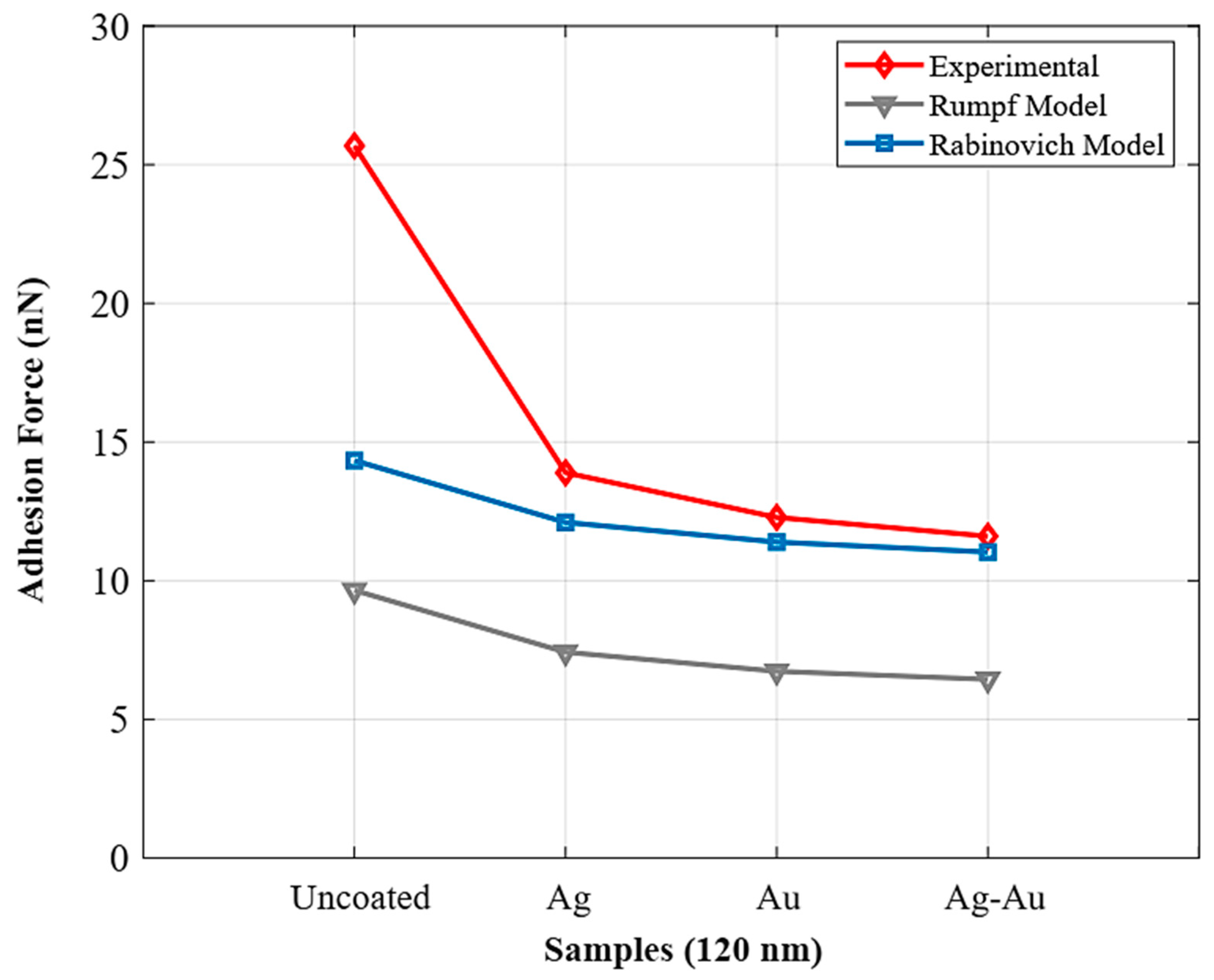
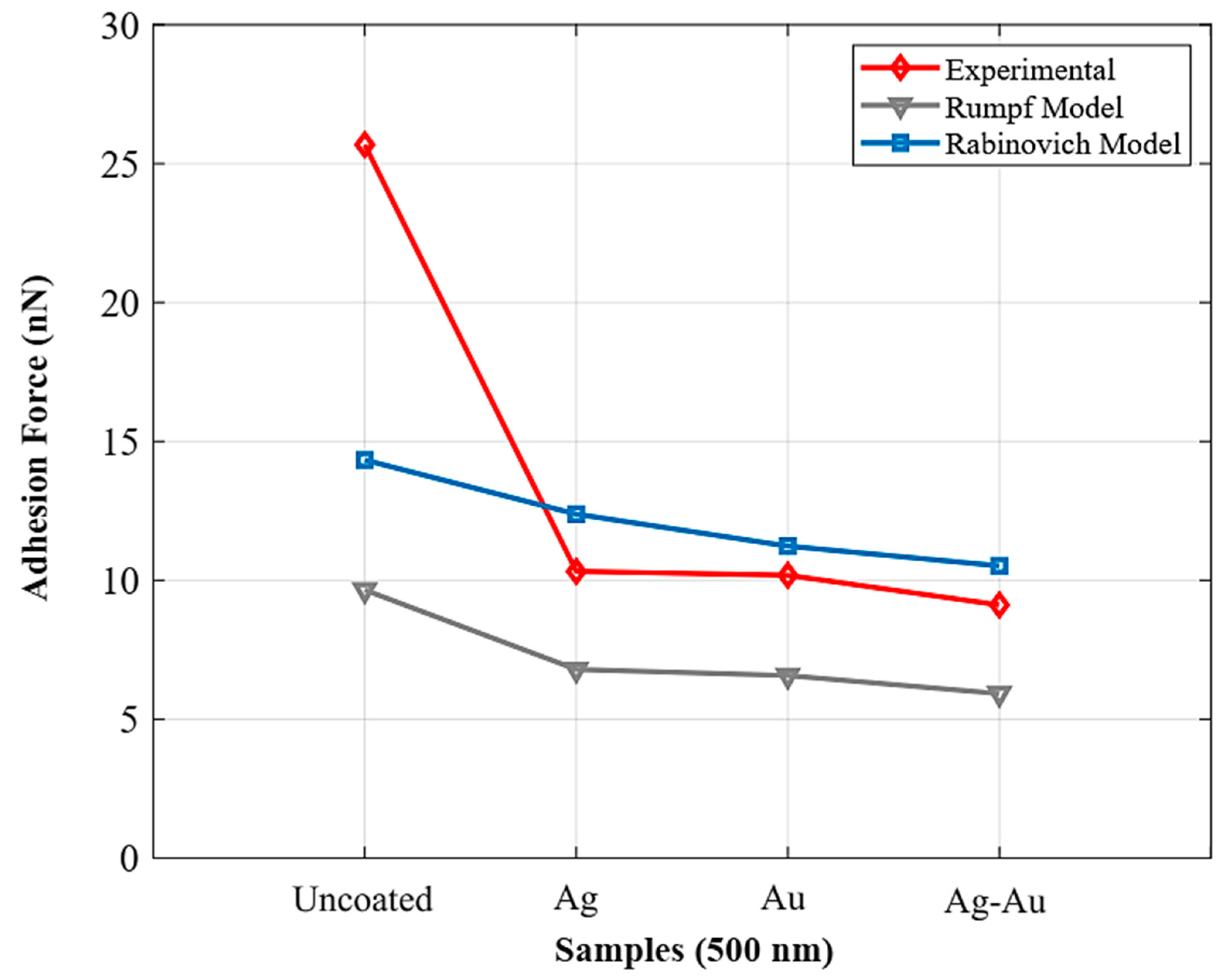
  • Comparing all coated samples with the non-coated ones suggests that reducing the adhesion force in all coated specimens is due to the reduction of surface energy and increased surface roughness. The surface energy of the gold on a silicon substrate is 1 J/mm2, and this value for silver on the silicon is 1.25 J/m2 [42,43]. According to the results, the highest roughness is related to the gold surface, which is an effective parameter in reducing adhesion due to the reduction of the contact surface [44,45]. In addition, the surface energy of gold is less than that of silver, which is a reason for the impact of surface energy on adhesion.
  • Theoretical and experimental adhesion values revealed that the compound thin films (500 nm) compared with the single thin films with the same thickness have higher surface roughness and the lowest adhesion force.
  • Both approaches indicated that gold coatings (single layer with thicknesses of 120 and 500 nm) compared to silver coatings with the same thicknesses have a drop in the adhesion force because of a reduction in surface energy and more surface roughness.
  • Comparing the adhesion values of Rumpf and Rabinovich models with the experimental ones revealed that the results achieved from the Rabinovich model were closer to the experimental values compared with the Rumpf model. This is due to moderately high surface energy and “soft” elastic materials with large tip radii.
  • One of the Rumpf model problems compared to Rabinovich is not determining the surface asperity radius, which was thought not feasible experimentally. Also, the Rumpf model cannot precisely measure the geometry of nanoscale surfaces [28].
  • Surface roughness and adhesion force results indicate that uncoated surfaces have higher adhesion force values than deposited surfaces. The increase in adhesion values is due to the atomic accumulation on the surface and the formation of asperities after the deposition process. The asperities lessen the tip contact with the surface. Consequently, the adhesion force decreases when the contact between tip and surface minimizes. In addition, the inverse effect of roughness on adhesion reduction can be observed when the roughness of the uncoated silicon surface is compared to the considerably lower adhesion of deposited surfaces.
  • As shown in Figure 10 and Table 4, the film with 500 nm thickness has less adhesion force than the sample with 120 nm thickness. The growth of atomic accumulation in the thickness of 500 nm has led to increased surface roughness and reduced adhesion. In other words, the change in the deposition thickness, surface energy, and roughness has a notable impact on the adhesion force.

4. Conclusions

In this study, Ag–Au compound coatings with thicknesses of 120 and 500 nm were fabricated on the surface of silicon substrates employing a novel method for manufacturing a compound sputtering target. Additionally, single layers of Ag and Au with the same thicknesses were deposited. Adhesion force, surface roughness, and morphology of thin films were measured by Rabinovich, Rumpf, and AFM. The investigations regarding the thickness effect indicate that increasing the thickness from 120 to 500 leads to a rise in surface roughness and a drop in adhesion force in single and compound films. Considering the theoretical adhesion models, it can be concluded that unlike Rumpf, the Rabinovich model presents closer values to the experimental method due to surface asperity radius. The results regarding the variation of the adhesion force revealed that the compound thin film has the lowest value obtained from both experimental and theoretical methods suggesting that this novel method can be utilized for coating compound layers on microgrippers’ surfaces where a reduction in adhesion force is intended.

Author Contributions

Conceptualization, M.S. and P.H.; methodology, B.R. and A.K.; formal analysis, M.S. and B.R.; investigation, P.H. and A.K.; data curation, V.P. and S.C.; writing—original draft preparation, M.S. and P.H.; supervision, V.P. and S.C. All authors have read and agreed to the published version of the manuscript.

Funding

This research received no external funding.

Institutional Review Board Statement

Not applicable.

Informed Consent Statement

Not applicable.

Data Availability Statement

Data is contained within the article.

Conflicts of Interest

The authors declare no conflict of interest. The funders had no role in the design of the study; in the collection, analyses, or interpretation of data; in the writing of the manuscript, or in the decision to publish the results.

References

  1. Ejeian, F.; Azadi, S.; Razmjou, A.; Orooji, Y.; Kottapalli, A.; Ebrahimi Warkiani, M.; Asadnia, M. Design and applications of MEMS flow sensors: A review. Sens. Actuators Phys. 2019, 295, 483–502. [Google Scholar] [CrossRef]
  2. Nastro, A.; Ferrari, M.; Ferrari, V. Double-actuator position-feedback mechanism for adjustable sensitivity in electrostatic-capacitive MEMS force sensors. Sens. Actuators Phys. 2020, 312, 112127. [Google Scholar] [CrossRef]
  3. Ali, W.R.; Prasad, M. Piezoelectric MEMS based acoustic sensors: A review. Sens. Actuators A Phys. 2020, 301, 111756. [Google Scholar] [CrossRef]
  4. Basu, A.K.; Basu, A.; Bhattacharya, S. Micro/Nano fabricated cantilever based biosensor platform: A review and recent progress. Enzyme Microb. Technol. 2020, 139, 109558. [Google Scholar] [CrossRef]
  5. Di Barba, P.; Wiak, S. MEMS: Field Models and Optimal Design; Springer International Publishing: New York, NY, USA, 2020; Volume 573, ISBN 978-3-030-21495-1. [Google Scholar]
  6. Paulasto-Kröckel, M.; Tilli, M.; Ross, G.; Kuisma, H. Where is silicon based MEMS heading to? In Handbook of Silicon Based MEMS Materials and Technologies, 3rd ed.; Micro and Nano Technologies; Tilli, M., Paulasto-Krockel, M., Petzold, M., Theuss, H., Motooka, T., Lindroos, V., Eds.; Elsevier: Amsterdam, The Netherlands, 2020; pp. xxi–xxix. ISBN 978-0-12-817786-0. [Google Scholar]
  7. Janioud, P.; Poulain, C.; Koumela, A.; Armani, J.M.; Dupret, A.; Rey, P.; Berthelot, A.; Jourdan, G.; Morfouli, P. Effects of gamma radiation on suspended silicon nanogauges bridge used for MEMS transduction. Microelectron. Reliab. 2020, 114, 113736. [Google Scholar] [CrossRef]
  8. Das, T.K.; Shirinzadeh, B.; Ghafarian, M.; Al-Jodah, A.; Zhong, Y.; Smith, J. Design, analysis and experimental investigations of a high precision flexure-based microgripper for micro/nano manipulation. Mechatronics 2020, 69, 102396. [Google Scholar] [CrossRef]
  9. Alogla, A.F.; Amalou, F.; Balmer, C.; Scanlan, P.; Shu, W.; Reuben, R.L. Corrigendum to “Micro-tweezers: Design, fabrication, simulation and testing of a pneumatically actuated micro-gripper for micromanipulation and microtactile sensing. Sens. Actuators Phys. 2018, 273, 324. [Google Scholar] [CrossRef]
  10. Verotti, M.; Dochshanov, A.; Belfiore, N.P. A comprehensive survey on microgrippers design: Mechanical structure. J. Mech. Des. Trans. ASME 2017, 139, 1–46. [Google Scholar] [CrossRef]
  11. Van Nguyen, P.; Luu, Q.K.; Takamura, Y.; Ho, V.A. Wet Adhesion of Micro-Patterned Interfaces for Stable Grasping of Deformable Objects. In Proceedings of the 2020 IEEE/RSJ International Conference on Intelligent Robots and Systems (IROS), Las Vegas, NV, USA, 24 October–24 January 2021; pp. 9213–9219. [Google Scholar]
  12. Feng, Y.Y.; Chen, S.J.; Hsieh, P.H.; Chu, W.T. Fabrication of an electro-thermal micro-gripper with elliptical cross-sections using silver-nickel composite ink. Sens. Actuators Phys. 2016, 245, 106–112. [Google Scholar] [CrossRef]
  13. Ardito, R.; Frangi, A.; Rizzini, F.; Corigliano, A. Evaluation of adhesion in microsystems using equivalent rough surfaces modeled with spherical caps. Eur. J. Mech. A/Solids 2016, 57, 121–131. [Google Scholar] [CrossRef]
  14. Llewellyn-Evans, H.; Griffiths, C.A.; Fahmy, A. Microgripper design and evaluation for automated µ-wire assembly: A survey. Microsyst. Technol. 2020, 26, 1745–1768. [Google Scholar] [CrossRef] [Green Version]
  15. Delrio, F.W.; Carraro, C.; Maboudian, R. Small-scale surface engineering problems. Tribol. Dyn. Engine Powertrain Fundam. Appl. Futur. Trends 2010, 960–989. [Google Scholar] [CrossRef]
  16. Demaghsi, H.; Mirzajani, H.; Ghavifekr, H.B. Design and simulation of a novel metallic microgripper using vibration to release nano objects actively. Microsyst. Technol. 2014, 20, 65–72. [Google Scholar] [CrossRef]
  17. Shao, G.; Ware, H.O.T.; Huang, J.; Hai, R.; Li, L.; Sun, C. 3D printed magnetically-actuating micro-gripper operates in air and water. Addit. Manuf. 2021, 38, 101834. [Google Scholar] [CrossRef]
  18. Adachi, H.; Wasa, K. Thin Films and Nanomaterials. In Handbook of Sputter Deposition Technology: Fundamentals and Applications for Functional Thin Films, Nano-Materials and MEMS, 2nd ed.; William Andrew: New York, NY, USA, 2012; pp. 3–39. [Google Scholar] [CrossRef]
  19. Behera, R.R.; Das, A.; Hasan, A.; Pamu, D.; Pandey, L.M.; Sankar, M.R. Effect of TiO2 addition on adhesion and biological behaviour behavior of BCP-TiO2 composite films deposited by magnetron sputtering. Mater. Sci. Eng. C 2020, 114, 111033. [Google Scholar] [CrossRef] [PubMed]
  20. Barajas-Valdes, U.; Suárez, O.M. Nanomechanical properties of thin films manufactured via magnetron sputtering from pure aluminum and aluminum-boron targets. Thin Solid Films 2020, 693, 137670. [Google Scholar] [CrossRef]
  21. Butt, H.J.; Cappella, B.; Kappl, M. Force measurements with the atomic force microscope: Technique, interpretation and applications. Surf. Sci. Rep. 2005, 59, 1–152. [Google Scholar] [CrossRef] [Green Version]
  22. Giessibl, F.J. Seizo Morita Noncontact Atomic Force Microscopy; Springer: Cham, Switzerland, 2015; Volume 3, ISBN 9783319155876. [Google Scholar]
  23. Ono, K.; Mizushima, Y.; Furuya, M.; Kunihisa, R.; Tsuchiya, N.; Fukuma, T.; Iwata, A.; Matsuki, A. Direct measurement of adhesion force of individual aerosol particles by atomic force microscopy. Atmosphere 2020, 11, 489. [Google Scholar] [CrossRef]
  24. Leite, F.L.; Bueno, C.C.; Da Róz, A.L.; Ziemath, E.C.; Oliveira, O.N. Theoretical models for surface forces and adhesion and their measurement using atomic force microscopy. J. Mol. Sci. 2012, 23, 12773–12856. [Google Scholar] [CrossRef]
  25. Prokopovich, P.; Perni, S. Comparison of JKR- and DMT-based multi-asperity adhesion model: Theory and experiment. Colloids Surf. Physicochem. Eng. Asp. 2011, 383, 95–101. [Google Scholar] [CrossRef]
  26. Prokopovich, P.; Starov, V. Adhesion models: From single to multiple asperity contacts. Adv. Colloid Interface Sci. 2011, 168, 210–222. [Google Scholar] [CrossRef]
  27. Rabinovich, Y.I.; Adler, J.J.; Ata, A.; Singh, R.K.; Moudgil, B.M. Adhesion between nanoscale rough surfaces. I. Role of asperity geometry. J. Colloid Interface Sci. 2000, 232, 10–16. [Google Scholar] [CrossRef] [PubMed]
  28. Beach, E.R.; Tormoen, G.W.; Drelich, J.; Han, R. Pull-off force measurements between rough surfaces by atomic force microscopy. J. Colloid Interface Sci. 2002, 247, 84–99. [Google Scholar] [CrossRef] [PubMed]
  29. Rumpf, H. Particle Technology; Springer Science & Business Media: Berlin/Heidelberg, Germany, 2012; Volume 1, ISBN 9401179441. [Google Scholar]
  30. Buranich, V.; Pogrebnjak, A.; Budzynski, P.; Shelest, I.; Prószyński, A.; Chocyk, D.; Goncharov, A.; Yunda, A. Mechanical and tribological characterization of nanostructured HfB2 films deposited from compound target. SN Appl. Sci. 2020, 2, 563. [Google Scholar] [CrossRef] [Green Version]
  31. Ma, D.L.; Liu, H.Y.; Deng, Q.Y.; Yang, W.M.; Silins, K.; Huang, N.; Leng, Y.X. Optimal target sputtering mode for aluminum nitride thin film deposition by high power pulsed magnetron sputtering. Vacuum 2019, 160, 410–417. [Google Scholar] [CrossRef]
  32. Baolong, G.; Deyi, L.; Jiajun, Z.; Wulin, Y.; Licai, F.; Lingping, Z. Construction of magnetron sputtering non-equilibrium Miedema’s model for application in Ag-Mo thin films. Phys. B Condens. Matter 2021, 602, 412541. [Google Scholar] [CrossRef]
  33. Vladkova, T.; Angelov, O.; Stoyanova, D.; Gospodinova, D.; Gomes, L.; Soares, A.; Mergulhao, F.; Ivanova, I. Magnetron co-sputtered TiO2/SiO2/Ag nanocomposite thin coatings inhibiting bacterial adhesion and biofilm formation. Surf. Coat. Technol. 2020, 384, 125322. [Google Scholar] [CrossRef]
  34. Francq, R.; Snyders, R.; Cormier, P.A. Structural and Morphological study of ZnO-Ag thin films synthesized by reactive magnetron co-sputtering. Vacuum 2017, 137, 1–7. [Google Scholar] [CrossRef]
  35. Mertin, S.; Länzlinger, T.; Sandu, C.S.; Scartezzini, J.-L.; Muralt, P. Combinatorial study of low-refractive Mg–F–Si–O nano-composites deposited by magnetron co-sputtering from compound targets. Appl. Surf. Sci. 2018, 435, 170–177. [Google Scholar] [CrossRef]
  36. Mazur, M.; Domaradzki, J.; Wojcieszak, D.; Kaczmarek, D. Investigations of elemental composition and structure evolution in (Ti, Cu)-oxide gradient thin films prepared using (multi) magnetron co-sputtering. Surf. Coat. Technol. 2018, 334, 150–157. [Google Scholar] [CrossRef]
  37. Annesi, F.; Pane, A.; Pezzi, L.; Pagliusi, P.; Losso, M.A.; Stamile, B.; Qualtieri, A.; Desiderio, G.; Contardi, M.; Athanassiou, A.; et al. Biocompatible and biomimetic keratin capped Au nanoparticles enable the inactivation of mesophilic bacteria via photo-thermal therapy. Colloids Surf. Physicochem. Eng. Asp. 2021, 625, 126950. [Google Scholar] [CrossRef]
  38. Xu, Y.; Wang, H.Z. Influence of Au doping concentration on structural and optical properties of ZnO:Au films fabricated through magnetron sputtering. Opt. Mater. 2020, 108, 110433. [Google Scholar] [CrossRef]
  39. Moghayedi, M.; Goharshadi, E.K.; Ghazvini, K.; Ahmadzadeh, H.; Jorabchi, M.N. Antibacterial activity of Ag nanoparticles/phosphomolybdate/reduced graphene oxide nanocomposite: Kinetics and mechanism insights. Mater. Sci. Eng. B 2020, 262, 114709. [Google Scholar] [CrossRef]
  40. Huang, W.; Tao, F.; Li, F.; Mortimer, M.; Guo, L.-H. Antibacterial nanomaterials for environmental and consumer product applications. NanoImpact 2020, 20, 100268. [Google Scholar] [CrossRef]
  41. Eichenlaub, S.; Chan, C.; Beaudoin, S.P. Hamaker constants in integrated circuit metalization. J. Colloid Interface Sci. 2002, 248, 389–397. [Google Scholar] [CrossRef] [Green Version]
  42. Zhang, J.-M.; Ma, F.; Xu, K.-W. Calculation of the surface energy of FCC metals with modified embedded-atom method. Appl. Surf. Sci. 2004, 229, 34–42. [Google Scholar] [CrossRef]
  43. Maugis, D. Adhesion of spheres: The JKR-DMT transition using a dugdale model. J. Colloid Interface Sci. 1992, 150, 243–269. [Google Scholar] [CrossRef]
  44. Rusu, F.; Pustan, M.; Bîrleanu, C.; Müller, R.; Voicu, R.; Baracu, A. Analysis of the surface effects on adhesion in MEMS structures. Appl. Surf. Sci. 2015, 358, 634–640. [Google Scholar] [CrossRef]
  45. Katainen, J.; Paajanen, M.; Ahtola, E.; Pore, V.; Lahtinen, J. Adhesion as an interplay between particle size and surface roughness. J. Colloid Interface Sci. 2006, 304, 524–529. [Google Scholar] [CrossRef]
Figure 1. Schematic representation of a sputtering target. Unlike the blue zone, the red part is involved in the deposition process.
Coatings 11 01551 g001
Figure 2. The compound target of Ag–Au.
Coatings 11 01551 g002
Figure 3. Schematic representation of the magnetron sputtering method with a compound sputtering target.
Coatings 11 01551 g003
Figure 4. (a) Silicon substrate with Ag and Au single layers, (b) Silicon substrate with Ag–Au compound layer.
Coatings 11 01551 g004
Figure 5. Three-dimensional topographies of the uncoated surface (a), silver surface (b,c), gold surface (d,e), and Ag–Au compound surface (f,g). (a) uncoated silicon substrate. (b) Silver coating with a thickness of 120 nm. (c) Silver coating with a thickness of 500 nm. (d) Gold coating with a thickness of 120 nm. (e) Gold coating with a thickness of 500 nm. (f) Compound coating with a thickness of 120 nm. (g) Compound coating with a thickness of 500 nm.
Coatings 11 01551 g005
Figure 6. A force-distance curve from the atomic force microscope (AFM).
Coatings 11 01551 g006
Figure 7. The image of gold thin film obtained by Gwyddion software.
Coatings 11 01551 g007
Figure 8. The graphs of the chosen effective points of the coated surfaces (a) Ag–Au 120 nm, and (b) Ag–Au 500 nm.
Coatings 11 01551 g008
Figure 9. Comparison of adhesion force values between theoretical and experimental approaches to samples with 120 nm thickness.
Coatings 11 01551 g009
Figure 10. Comparison of adhesion force values between theoretical and experimental approaches to samples with 500 nm thickness.
Coatings 11 01551 g010
Table 1. The deposition conditions for coating Ag, Au, and Ag–Au thin films.
Final Pressure (mbar)Argon Pressure (mbar)Voltage (V)Temperature (°C)Target-Substrate Distance (mm)Substrate Dimensions (mm2)
2.5 × 10−59 × 10−36007013010 × 10
Table 2. Surface parameters of silver and gold single layers and Ag–Au compound layers.
SamplesRa (nm)Rms (nm)Height of Asperities (nm)
120500120500120500
Ag0.4561.030.8171.98412.81.984
Au0.5331.090.8252.99412.12.994
Ag–Au0.8781.231.2963.56416.63.564
Si (uncoated)0.3950.8248.4
Table 3. Hamaker coefficient of the surfaces [41].
SurfaceHamaker Coefficient
A H 12 ( A / 10 20 J )  
Si-Si31.60
Ag-Ag50.00
Au-Au40.00
Si-Ag39.75
Si-Au35.55
Ag-Au44.72
Table 4. The average force values of single and compound thin films were obtained by theoretical and experimental approaches for 120 and 500 nm thicknesses.
SamplesThickness (nm)Experimental Adhesion Force (nN)Mean Values of Theoretical Adhesion Force (nN)
RumpfRabinovich
uncoated-25.689.6514.33
Ag12013.897.4212.10
Au12012.286.7311.39
Ag–Au12011.606.4411.03
Ag50010.326.7912.38
Au50010.186.5711.23
Ag–Au5009.115.9210.52
Publisher’s Note: MDPI stays neutral with regard to jurisdictional claims in published maps and institutional affiliations.

