Abstract
An integrated functional anti-reflective surface is of great significance for optical and optoelectronic devices. Hence, its preparation has attracted great attention from many researchers. This study combined wet alkaline etching approaches and reactive ion etching (RIE) techniques to create a dual-scale hierarchical anti-reflective surface on silicon substrates. The effect of RIE time on surface morphology and optical performance was investigated using multiple characterization forms. The optimal parameters for the fabrication of dual-scale structures by the composite etching process were explored. The silicon surface with a dual-scale structure indicated excellent anti-reflective properties (minimum reflectivity of 0.9%) in the 300 to 1100 nm wavelength range. In addition, the ultra-low reflection characteristic of the surface remained prominent at incident light angles up to 60°. The simulated spectra using the finite difference time domain (FDTD) method agreed with the experimental results. Superhydrophobicity and self-cleaning were also attractive properties of the surface. The functionally integrated surface enables silicon devices to have broad application prospects in solar cells, light emitting diodes (LEDs), photoelectric detectors, and outdoor equipment.
1. Introduction
Silicon is one of the most abundant materials on Earth and has the characteristics of good chemical stability, no environmental pollution, easy doping, and easy purification [1,2,3,4,5]. It has been widely used in the semiconductor industry. Moreover, silicon is the most promising fundamental material in the microelectronics and solar photovoltaic industries [6,7,8,9,10]. However, with the development of technology, many critical problems have been exposed, such as narrow spectral absorption and high reflectivity. Therefore, it is worthwhile to explore the surface modification technology of silicon materials in depth. The surface of silicon has deficient average absorption in the visible–near-infrared spectral band. Since the last century, researchers have been seeking to improve the absorption coefficient of silicon in the visible–near-infrared spectral band by modifying the surfaces of silicon substrates [11,12,13]. In particular, the fabrication of micro-nano structures on the silicon surface is a popular route for surface modification [14,15,16,17,18,19,20,21]. For example, pyramidal structures effectively reduce the surface’s reflectivity and improve the efficiency of photovoltaic cells, which is attributed to their ability to collect and capture light through internal reflection [22,23,24,25,26,27,28,29,30].
The approaches to constructing micro-nano structures on silicon substrates have been categorized into two species: wet etching and dry etching. One of the conventional operations for wet etching is the anisotropic etching of silicon using alkaline chemicals (potassium hydroxide/sodium hydroxide). This method has the advantages of low cost, simple equipment, easy observation, easy operation, and easy preparation of large areas [2,31,32,33]. Dry etching uses an ion source with specific energy to bombard the substrate material and causes it to peel to achieve etching. With continuous development, dry etching has led to a variety of processes, such as reactive ion etching (RIE) [34,35,36,37], the inductively coupled plasma etching (ICP) process [38,39,40], the ion beam etching process, and deep reactive ion etching (DRIE) [41]. RIE is an etching method that produces both physical and chemical effects. The technique can be operated at room temperature and has the advantage of fast etching speed and high precision.
Here, we developed an ultra-low-reflectivity surface with unique wetting properties by combining wet etching methods with RIE techniques. The effect of RIE time on silicon surface morphology and optical properties with micro-nano dual-scale hierarchical structures was investigated. The optimal technical parameters for the fabrication of dual-scale structures by the RIE technique combined with the wet etching process were obtained. The optical property of the surface was simulated using the finite difference in the time domain (FDTD) method. Hydrophobicity and self-cleaning are also attractive properties of the surface. We also briefly compared this work with those recently reported, as shown in Table 1. The functionally integrated surface enables silicon devices to have broad application prospects in solar cells, LEDs, photoelectric detectors, and outdoor equipment.

Table 1.
Comparison of this work with recently reported work.
2. Experimental Section
2.1. Materials
Silicon wafer (20 × 20 × 5 mm3, the resistivity of 1~10 Ω cm, p-type, single-sided polished), isopropyl alcohol (IPA, AR ≥ 99.5%), potassium hydroxide (KOH), hydrofluoric acid (HF), anhydrous ethanol, acetone, deionized water, trifluoromethane (CHF3), sulfur hexafluoride (SF6), and helium (He).
2.2. Fabrication of Dual-Scale Hierarchical Micro-Nano-Structured Optical Surface
The silicon wafers were first ultrasonically cleaned using, in order, acetone, anhydrous ethanol, and deionized water. The purpose was to remove contaminants such as oil, particles, and metals left on the surface during manufacturing. Each solvent was cleaned in two cycles, each cycle lasting 10 min. The cleaned wafers were placed in a certain amount of HF to remove the oxide layer on the surface. The reaction time was 1 min, and the control temperature was 70 °C. The wafers with the oxide layer removed were wet-etched in a mixture of KOH and isopropanol for 15 min at a controlled temperature of 80 °C. After the wet reaction, the samples were washed with deionized water and blown dry with nitrogen.
Further to optimize the sample surface, the wet-etched samples were resurfaced by RIE. The samples were placed in a vacuum chamber, and the radio frequency (RF) power was set to 300 W. The gas reactant was a mixture containing CHF3/SF6/He. During the etching process, the chamber pressure was maintained at 5 Pa and the etching time was 5~25 min. Ultimately, exotic dual-scale structures were formed on the silicon surface after two etchings.
2.3. Performance Characterization
The morphology of the silicon wafers was analyzed by scanning electron microscopy (SEM, ZEISS FESEM ULTRA 55, Carl zeissNTS GmbH, Jena, Germany). Reflectance measurements at 300~1100 nm were performed using a UV–Vis–NIR spectrophotometer (PerkinElmer Lambda 950, PerkinElmer, Waltham, MA, USA). The surface wettability of the samples was characterized using a contact angle tester (JC2000C, Shanghai Zhongchen Digital Technology Co., Shanghai, China).
3. Results and Discussion
The schematic diagram in Figure 1 briefly illustrates the fabrication of the surface with micro-nano dual-scale structures. First, the silicon wafers <100> were anisotropically etched with alkaline solvent. The essence of the chemical reaction is the reaction between Si and :
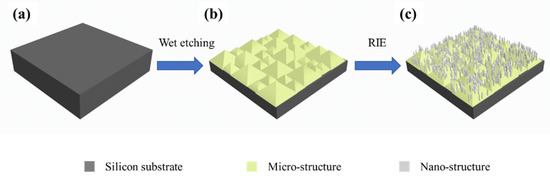
Figure 1.
The process of fabrication of dual-scale hierarchical optical structures on silicon. (a) Unetched silicon wafer (b) Wet etched silicon wafer (c) Further RIE etched wafer.
The generated silicon particles immediately afterward can undergo a complexation reaction with IPA, as shown in the following equation:
The complexation reaction products were proven to be highly soluble in water. Therefore, the anisotropic corrosion reaction of silicon wafers can be carried out continuously, leading to the final formation of the micro-scale pointed cone shape of the pyramid structure. However, the silicon surface properties of micro-scale pyramids have not yet fully achieved the goal of ultra-low reflection. The surface needs to be further optimized.
The next step was to execute the RIE of the above micron pyramid structure. During etching with CHF3/SF6/He plasma, there was constant competition between reactive fluorine ions (CFx+, SFx+) and passivated fluorocarbons (CFx). SF6 generates a glow discharge at a specific voltage and forms fluorine radicals (), which immediately react with silicon atoms on the sample surface to form volatile gas products. The chemical reaction equations are:
Under suitable RIE etching conditions, CFx was randomly deposited on the surface to act as a mask to prevent etching. Therefore, in the RIE, two processes co-occur: fluorocarbon deposition and etching. Helium was added for two primary purposes: energy transfer and intermolecular spacing reduction. The balance of etching and fluorocarbon deposition can be used to fabricate nano-scale structures. The effective combination of wet etching and reactive ion etching produced a micro-nano dual-scale surface.
3.1. Fabrication of Micro-Scale Pyramidal Structure
The morphological structure of the silicon wafers after wet etching was observed using SEM. Figure 2a and the inset show the sample’s top and side-view SEM images after anisotropic alkaline etching, respectively. It can be noticed that micro-scale structures with distinctive characteristics are presented on the surface of the bare silicon wafer. Viewed as a whole, the micro-scale structures are compactly arranged, and the substrate is thoroughly covered. Individually, the angles are well-defined and exhibit a conspicuous pyramidal feature. Figure 2b compares the reflection spectra of the bare silicon wafer and the silicon wafers equipped with micro-scale structures in the wavelength range of 300~1100 nm. Wet etching can effectively reduce the reflectance in the broadband wavelength. The average reflectance is reduced by 23.72%. From the perspective of geometrical optics, when the incident light arrives at the surface of a bare silicon wafer, there is only one reflection, and the incident light is absorbed once. However, at least two reflections occur when the incident light reaches a surface with a micron pyramidal structure, and the sunlight is absorbed at least twice. The wet etching approach to fabricate micro-scale anti-reflective structures provided a favorable basis for the subsequent preparation of dual-scale forms.
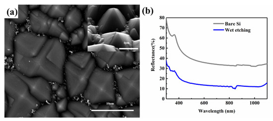
Figure 2.
(a) SEM image of the silicon wafer after wet etching. (b) Reflectance spectra of the bare wafer and wet etched wafer.
3.2. Fabrication of Dual-Scale Hierarchical Structures
We obtained dual-scale structures with excellent anti-reflective properties by further sculpting the nano-scale structure on the micro-scale structure through RIE. During RIE, the etching time directly affects the density and size of the nanostructure, which ultimately affects the anti-reflective properties of the silicon surface. To explore the effect of RIE time on the anti-reflective properties of the silicon surface more quickly, we first performed the RIE operation on bare silicon wafers and characterized the morphology and reflection spectra of different samples.
Figure 3 shows the surface morphology and anti-reflective properties of the sample treated by one-step reactive ion etching solely, and the experimental parameters are detailed in Table 2. Figure 3a–d show the SEM images of the samples at RIE times of 10 min, 15 min, 20 min, and 25 min, respectively. As shown in Figure 3a, when the reactive ion etching process lasted for 10 min, the entire surface of the silicon wafer was almost uniformly distributed by fluorocarbons. At the same time, some nanostructures appear, which are sparsely arranged with large average spacing. As the etching time increases to 15 min, the number of new nanodots on the surface increases and the nanostructures become tightly arranged, as demonstrated in Figure 3b. However, the strength between the fluorocarbon deposition effect and the etching effect changes as the time increases during the reactive ion etching process. When the reaction time is extended to 20 min, the etching effect is stronger than the fluorocarbon deposition effect. Thus, the size of the nanostructures in Figure 3c is larger than that in Figure 3b. When the etching time is 25 min, it can be noticed from Figure 3d that the density of the nanostructures becomes smaller and the size becomes larger, and these changes are due to the annexation effect between adjacent structures.
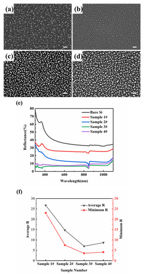
Figure 3.
RIE with different etching times: SEM of samples (a) 10 min, (b) 15 min, (c) 20 min, (d) 25 min; (e) reflectance spectra of different samples; (f) average R and minimum R plot for samples with different RIE etching times. Scale bars 1 μm.
Table 2.
Samples etched with different RIE times.
The samples treated under different conditions differed not only in morphology but also in anti-reflective properties. As shown in Figure 3e,f, the average reflectance decreased by approximately 12% when the etching time was increased from 10 to 15 min. After 20 min of RIE, the average reflectance of the sample again decreased by 7.73%. When the etching time lasted for 25 min, the average reflectance increased by 1.72%. The surface of the sample after 20 min of etching had the lowest reflectance of 3.57%. Overall, the average reflectance and the minimum reflectance show a trend of decreasing and then increasing with prolongation of the etching time, which is consistent with the pattern of structural changes.
The RIE time parameter altered the surface structure and had an impact on performance. We repeated RIE on the wet-etched samples to create dual-scale micro-nano hierarchical structures on the silicon based on the above experimental results. Figure 4a–d show the SEM of the sample surface under different combination etching parameters. The details of the combination process parameters are shown in Table 3. Figure 4a–d correspond to RIE times of 10 min, 15 min, 20 min, and 25 min, respectively. The rough morphology emerged during the etching process as the fluorocarbon was further deposited on the wet-etched micrometer pyramidal structure. RIE was treated for 10 min, and the micro-scale pyramidal structure from the previous wet etching step in Figure 4a had a distinctive structure with well-defined angles. The nano-scale structures obtained by RIE were uniformly and densely distributed. With the increase in etching time, the micro-scale pyramidal structure of the whole surface did not change significantly; however, the nano-scale structure became denser and larger than when treated for 10 min. The distance between the nano-scale structures was slightly larger than the diameter of the nanostructures. These details are shown in Figure 4b. Continuing to deepen the etching, the pyramid shape was still evident, and the nano-scale structures were larger and more uniform in size. Figure 4c shows the top view of the SEM at an etching time of 20 min, while Figure 4e shows the corresponding cross-sectional SEM image, from which we can visualize the dual-scale feature of the structure. However, after the etching time was greater than 20 min, the etching deepened, the adjacent nano-scale structures were aggregated, and the outline of the micro-scale pyramid was destroyed and became softened.
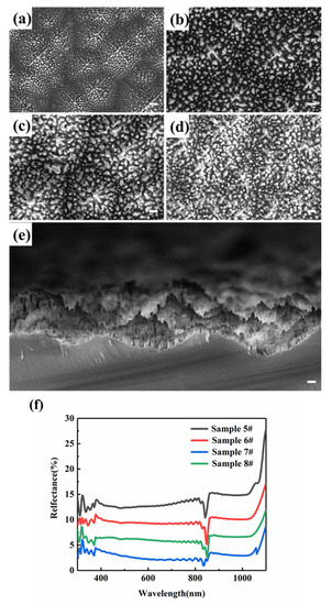
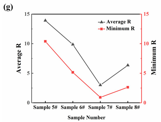
Figure 4.
Morphology and reflectance spectral information of dual-scale structures: SEM of samples with different RIE times (a) 10 min, (b) 15 min, (c) 20 min, (d) 25 min; (e) SEM cross-sectional view of sample with optimal etching parameters, scale bars 1 μm; (f) reflectance spectra of different samples; (g) average R and minimum R plot for different samples.
Table 3.
Samples etched by wet etching and at different RIE times.
The reflectance spectral data of the samples for various combined etching conditions are given in Figure 4f,g. When the etching time was extended from 10 min to 20 min, the dense and increasing nano-scale structures played a role, and the reflectivity decreased by 10.92% on average. However, when the etching time exceeded 20 min, the effect of the micro-scale pyramids in reducing reflection was eliminated, and the reflectivity increased by an average of 3.35%. The lowest reflectivity of 0.92% was achieved when the etching time was 20 min, which was the optimal time parameter.
Based on the above experimental results, we summarized the basic mechanism of the effect of etching time on the reflectivity of the dual-scale structure. The RIE process was a process in which two reactions, fluorocarbon deposition and etching, were carried out simultaneously and competed. The relative intensities of the deposition and etching processes were in the process of change with different etching times. When the deposition of fluorocarbon dominated, the nanodots in the structure increased, and the density of the nanostructure changed more significantly. While when the etching process played a major role, the size of the nanostructure changed more significantly. It was precisely the variability of these two processes that gave rise to the variability of the dual-scale structure with the etching time, and ultimately to the different anti-reflective properties.
3.3. Optical Properties of Surfaces with Dual-Scale Hierarchical Structures
Photographs of the samples treated with the different etching processes were captured under natural light. Figure 5a can be described as follows. The original silicon wafer on the far left intensely reflected natural light and could mirror clear text. Next was the silicon wafer etched by wet etching. The silicon wafer etched by one-step RIE was relegated to the third position, and the silicon wafer with dual-scale structures prepared by the composite process was placed on the far right, and it was clearly the darkest of the four samples, with the lowest reflectivity. The reflectance spectra corresponding to the four physical samples are given in Figure 5b. The silicon wafer’s high refractive index results in an average surface reflectance of more than 35%. After wet etching, the average reflectivity of the silicon wafer surface was reduced by nearly 61%, with a minimum reflectivity of 9.81%. Further, the reflectance reduction of the sample after one-step dry etching was also well-demonstrated. The average reflectance was 6.97% in the 300~1100 nm band. The composite etched samples had the finest anti-reflective properties. The average reflectance in the UV–Vis–NIR band was 2.99%, and the lowest reflectance was 0.92%. The dual-scale structure derived from both wet and dry etching processes, which traps the light, is intrinsic to the low reflectivity performance.
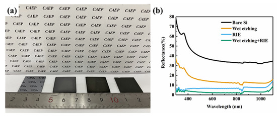
Figure 5.
(a) Photographs of the samples treated by different etching processes were captured under natural light. (b) Reflectance spectra corresponding to the samples in Figure 5a.
Thus, we theoretically simulated the anti-reflection properties of the dual-scale hierarchical structure using the commercial software FDTD version 2019. First, the whole surface was divided into two layers: the lower layer was the silicon substrate layer, and the upper layer was the etched dual-scale structure. Among them, the dimensional parameters of the dual-scale structure were set as a micron pyramid with a height and width of L = 5 μm, and the nano-scale structure was a cone with a variable bottom diameter (d = 50 nm~200 nm) and height (h = 450 nm~700 nm). It was noticed that the micron-scale pyramids in the simulation model were arranged periodically, while the uppermost nanoscale structures were randomly distributed. Material settings for pyramid structure, nanoscale structure, and substrate structure were set to “Si (Silicon) Palik”. The filling medium between each different structure was air. The incident light source was a plane-wave light source with a wavelength band of 300~1100 nm and a Z-axis negative direction. The grid size was set to: dx = 5 nm, dy = 5 nm, dz = 10 nm. Regarding the boundary conditions, the X and Y directions were set to "Bloch", and the Z direction was set to "PML". The reflectivity detector was placed at the boundary of the simulation area and the light source. Figure 6a shows the schematic diagram of the simulation model. After data comparison, the reflectance and absorption data of the simulation model with dimensions (h = 600 nm, d = 60 nm) were close to the measured results of the dual-scale hierarchical structure shown in Figure 4e. The comparison results are shown in Figure 6c,d, respectively. Figure 6b displays the electric field intensity map of the wavelength at 590 nm (this wavelength corresponds to the lowest reflectivity). All in all, it has been demonstrated both theoretically and experimentally that the prepared dual-scale hierarchical structure was a low-reflection and high-absorption structure.
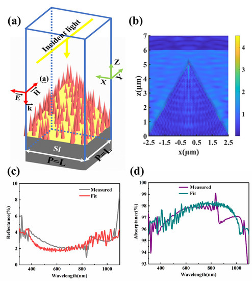
Figure 6.
(a) Schematic diagram of simulation model; (b) the electric field intensity map of the XZ plane λ = 590 nm (this wavelength corresponds to the lowest reflectivity); (c) simulation and experimental reflection spectra of dual-scale micro-nano hierarchical structure; (d) simulation and experimental absorption spectra of dual-scale micro-nano hierarchical structure.
The ultra-low reflection of the surface with dual-scale hierarchical structures occurred not only in a wide wavelength range from 300 to 1100 nm but also at large angular incidence of the light. Figure 7 shows the specular reflectance of the hierarchical structure for angles of incidence varying from 0° to 75°. The specular reflectance of these optimized dual-scale structures remained below 1% even at angles as high as 60°. The high tolerance to the angle of incident light will facilitate the maximization of light absorption by solar cells without actively tracking sunlight.
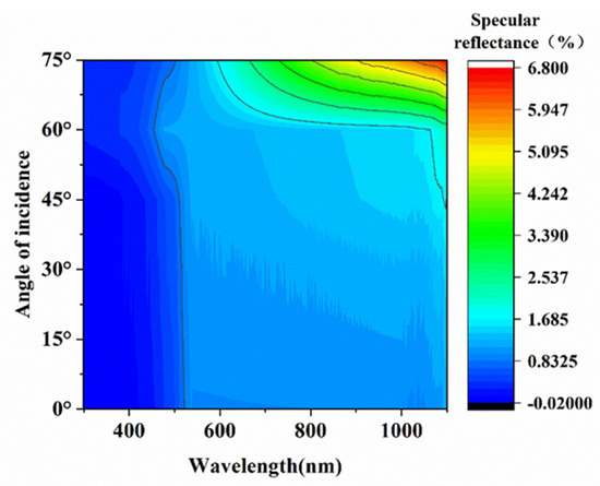
Figure 7.
Contour plots of specular reflectance of dual-scale micro-nano hierarchical structures at different angles of incidence.
3.4. Wettability of Surfaces with Dual-Scale Hierarchical Structures
The superhydrophobicity of silicon devices is of great importance in various practical applications owing to their fascinating self-cleaning properties. To evaluate the wettability of the dual-scale hierarchical structured silicon surface, water contact angle (WCA) measurements were carried out. Figure 8a shows the water contact angle measurement of 105.54° for the sample etched by wet etching only, which corresponds to the surface of a micro-scale pyramidal structure. Figure 8b shows the WCA measurement of 152.31° for the sample etched by wet etching and then by RIE. The test results clearly show that the surface with the micro-nano dual-scale structure exhibits superhydrophobicity. In practice, contaminants and dust adhering to a superhydrophobic surface are easily washed off by water, so the surface exhibits self-cleaning properties.
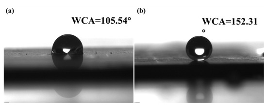
Figure 8.
WCA test results of different samples: (a) wet-etched, (b) wet etching and RIE combined.
4. Conclusions
In conclusion, dual-scale anti-reflective structures were prepared by a combination of the wet etching process and RIE technology. The anti-reflection performance of the surface was optimal when the RIE time was 20 min under the conditions of invariable gas flow rate and RF power. The micro-scale pyramidal and the nano-scale structures were perfectly combined in scale and position, enabling the silicon device’s surface to absorb light from all directions. Silicon surfaces with a dual-scale hierarchical structure exhibited excellent anti-reflection properties in the wide wavelength range of 300 to 1100 nm, with a minimum reflectance of 0.92%. In particular, the ultra-low anti-reflection property of the surface was highly tolerant to the incident light angle, which was still apparent at incident light angles as high as 60°. Simultaneously, due to the existence of the dual-scale structure, the silicon wafer surface acquired superhydrophobic properties, and the whole device had the capability of self-cleaning. This work demonstrates that the combination of wet etching and RIE techniques to prepare such dual-scale structures is standard and feasible. It provides an effective solution for large area preparation of integrated functional silicon devices. However, the surface mechanical properties of devices with dual-scale structures should be further improved.
Author Contributions
Conceptualization, M.D.; methodology, Z.Y. and X.Y.; software, M.D., N.Z., J.C. and Z.L.; validation, N.Z., J.C. and Z.L.; investigation, Y.Z.; data curation, N.Z.; writing—original draft preparation, M.D.; writing—review and editing, M.D. and J.W.; visualization, M.D. and Y.Z.; supervision, Z.Y. and X.Y.; project administration, X.Y.; funding acquisition, X.Y. All authors have read and agreed to the published version of the manuscript.
Funding
The work is supported by the Innovation and Development Foundation of China Academy of Engineering Physics (grant number: CX20200021), and the Scientific Research Fund of SiChuan Provincial Science and Technology Department (grant number: 2020YJ0137).
Institutional Review Board Statement
Not applicable.
Informed Consent Statement
Not applicable.
Data Availability Statement
The study did not report any data.
Conflicts of Interest
The authors declare no conflict of interest.
References
- Ye, X.; Huang, J.; Ni, R.F.; Yi, Z.; Zheng, W.G. Broadband antireflection and self-cleaning random grass structure on silicon. J. Optoelectron. Adv. Mater. 2015, 17, 192–197. [Google Scholar]
- Zeng, Y.; Fan, X.; Chen, J.; He, S.; Yi, Z.; Ye, X.; Yi, Y. Preparation of composite micro/nano structure on the silicon surface by reactive ion etching: Enhanced anti-reflective and hydrophobic properties. Superlattices Microstruct. 2018, 117, 144–154. [Google Scholar] [CrossRef]
- Yang, C.; Jing, X.; Wang, F.; Ehmann, K.F.; Tian, Y.; Pu, Z. Fabrication of controllable wettability of crystalline silicon surfaces by laser surface texturing and silanization. Appl. Surf. Sci. 2019, 497, 143805. [Google Scholar] [CrossRef]
- Liu, S.; Niu, X.; Shan, W.; Lu, W.; Zheng, J.; Li, Y.; Duan, H.; Quan, W.; Han, W.; Wronski, C.R. Improvement of conversion efficiency of multicrystalline silicon solar cells by incorporating reactive ion etching texturing. Sol. Energy Mater. Sol. Cells 2014, 127, 21–26. [Google Scholar] [CrossRef]
- Chen, W.H.; Hong, C.N. 0.76% absolute efficiency increase for screen-printed multicrystalline silicon solar cells with nanostructures by reactive ion etching. Sol. Energy Mater. Sol. Cells 2016, 157, 48–54. [Google Scholar] [CrossRef]
- Rajkanan, K.; Singh, R.; Shewchun, J. Absorption coefficient of silicon for solar cell calculations—ScienceDirect. Solid-State Electron. 1979, 22, 793–795. [Google Scholar] [CrossRef]
- Saga, T. Advances in crystalline silicon solar cell technology for industrial mass production. Npg Asia Mater. 2010, 2, 96–102. [Google Scholar] [CrossRef]
- Huang, Z.; Carey, J.E.; Liu, M.; Guo, X.; Mazur, E.; Campbell, J.C. Microstructured silicon photodetector. Appl. Phys. Lett. 2006, 89, 516. [Google Scholar] [CrossRef]
- Beam, J.C.; Leblanc, G.; Gizzie, E.A.; Ivanov, B.L.; Needell, D.R.; Shearer, M.J.; Jennings, G.K.; Lukehart, C.M.; Cliffel, D.E. Construction of a Semiconductor–Biological Interface for Solar Energy Conversion: P-Doped Silicon/Photosystem I/Zinc Oxide. Langmuir Acs J. Surf. Colloids 2015, 31, 10002–10007. [Google Scholar] [CrossRef]
- Lee, C.; Bae, S.Y.; Mobasser, S.; Manohara, H. A novel silicon nanotips antireflection surface for the micro sun sensor. Nano Lett. 2005, 5, 2438–2442. [Google Scholar] [CrossRef]
- Zhang, D.; Ren, W.; Zhu, Z.; Zhang, H.; Liu, B.; Shi, W.; Qin, X.; Cheng, C. Highly-ordered silicon inverted nanocone arrays with broadband light antireflectance. Nanoscale Res. Lett. 2015, 10, 9. [Google Scholar] [CrossRef]
- Chang, L.; Qiu, R.; Wen, C.; Li, Z.; Hu, S. Microstructuring and doping of silicon with nanosecond laser pulses. Appl. Surf. Sci. 2012, 258, 8002–8007. [Google Scholar] [CrossRef]
- Davidsen, R.S.; Li, H.; To, A.; Wang, X.; Han, A.; An, J.; Colwell, J.; Chan, C.; Wenham, A.; Schmidt, M.S. Black silicon laser-doped selective emitter solar cell with 18.1% efficiency. Sol. Energy Mater. Sol. Cells 2016, 144, 740–747. [Google Scholar] [CrossRef]
- Cai, J.; Qi, L. Recent advances in antireflective surfaces based on nanostructure arrays. Mater. Horiz. 2015, 2, 37–53. [Google Scholar] [CrossRef]
- Leon, J.J.D.; Hiszpanski, A.M.; Bond, T.C.; Kuntz, J.D. Design Rules for Tailoring Antireflection Properties of Hierarchical Optical Structures. Adv. Opt. Mater. 2017, 5, 1700080. [Google Scholar] [CrossRef]
- Li, B.; Niu, G.; Yi, Y.; Zhou, X.W.; Liu, X.D.; Sun, L.X.; Wang, C.Y. Antireflection subwavelength structures based on silicon nanowires arrays fabricated by metal-assisted chemical etching. Superlattices Microstruct. 2017, 111, 57–64. [Google Scholar] [CrossRef]
- Deng, Z.; Yang, Q.; Chen, F.; Meng, X.; Bian, H.; Yong, J.; Shan, C.; Hou, X. Fabrication of large-area concave microlens array on silicon by femtosecond laser micromachining. Opt. Lett. 2015, 40, 1928–1931. [Google Scholar] [CrossRef] [PubMed]
- Dawood, M.K.; Liew, T.H.; Lianto, P.; Hong, M.H.; Tripathy, S.; Thong, J.; Choi, W.K. Interference lithographically defined and catalytically etched, large-area silicon nanocones from nanowires. Nanotechnology 2010, 21, 205305. [Google Scholar] [CrossRef] [PubMed]
- Zhang, Z.; Wang, Z.; Wang, D.; Ding, Y. Periodic antireflection surface structure fabricated on silicon by four-beam laser interference lithography. J. Laser Appl. 2013, 26, 012010. [Google Scholar] [CrossRef]
- Wen, C.; Li, X.; He, X.; Duan, X.; Hu, S. Microstructuring and doping of monocrystalline silicon with femtosecond and nanosecond laser pulses. High Power Laser Part. Beams 2015, 27, 228–234. [Google Scholar] [CrossRef]
- Liu, Y.; Das, A.; Lin, Z.; Cooper, I.B.; Rohatgi, A.; Wong, C.P. Hierarchical robust textured structures for large scale self-cleaning black silicon solar cells. Nano Energy 2014, 3, 127–133. [Google Scholar] [CrossRef]
- Gangopadhyay, U.; Kim, K.; Dhungel, S.K.; Basu, P.K.; Yi, J. Low-cost texturization of large-area crystalline silicon solar cells using hydrazine mono-hydrate for industrial use. Renew. Energy 2006, 31, 1906–1915. [Google Scholar] [CrossRef]
- Smith, A.W.; Rohatgi, A. Ray tracing analysis of the inverted pyramid texturing geometry for high efficiency silicon solar cells. Sol. Energy Mater. Sol. Cells 1993, 29, 37–49. [Google Scholar] [CrossRef]
- Akila, B.S.; Vaithinathan, K.; Balaganapathi, T.; Vinoth, S.; Thilakan, P. Investigations on the correlation between surface texturing histogram and the spectral reflectance of (100) Crystalline Silicon Substrate textured using anisotropic etching. Sens. Actuators A Phys. 2017, 263, 445–450. [Google Scholar] [CrossRef]
- Al-Husseini, A.M.; Lahlouh, B. Influence of pyramid size on reflectivity of silicon surfaces textured using an alkaline etchant. Bull. Mater. Sci. 2019, 42, 152. [Google Scholar] [CrossRef]
- Zhang, Y.P.; Wang, W.T.; Wang, C.; Yang, J. Study of optical anti-reflection characteristics based on nanometer “pyramid” structure. Laser Infrared 2018, 48, 215–220. [Google Scholar] [CrossRef]
- Lv, H.; Shen, H.; Ye, J.; Chao, G.; Han, Z.; Yuan, J. Porous-pyramids structured silicon surface with low reflectance over a broad band by electrochemical etching. Appl. Surf. Sci. 2012, 258, 5451–5454. [Google Scholar] [CrossRef]
- Ou, H.-F.; Lin, Y.-K.; Hsueh, C.-H. Structural and optical properties of textured silicon substrates by three-step chemical etching. Langmuir 2021, 37, 9622–9629. [Google Scholar] [CrossRef] [PubMed]
- Wang, P.; Liu, Z.; Xu, K.; Blackwood, D.J.; Hong, M.; Aberle, A.G.; Stangl, R.; Peters, I.M. Periodic upright nanopyramids for light management applications in ultrathin crystalline silicon solar cells. IEEE J. Photovolt. 2017, 7, 493–501. [Google Scholar] [CrossRef]
- Lou, R.; Zhang, G.; Li, G.; Li, X.; Liu, Q.; Cheng, G. Design and fabrication of dual-scale broadband antireflective structures on metal surfaces by using nanosecond and femtosecond lasers. Micromachines 2020, 11, 20. [Google Scholar] [CrossRef] [PubMed]
- Yoo, J.; Yu, G.; Yi, J. Black surface structures for crystalline silicon solar cells. Mater. Sci. Eng. B 2009, 159, 333–337. [Google Scholar] [CrossRef]
- Chen, J.; Deng, T.; Wu, C.N.; Liu, Z.W. Fabrication of silicon nanopore arrays with three-step wet etching. ECS Trans. 2013, 52, 371. [Google Scholar] [CrossRef]
- Munoz, D.; Carreras, P.; Escarre, J.; Ibarz, D.; Nicolas, S.M.D.; Voz, C.; Asensi, J.M.; Bertomeu, J. Optimization of KOH etching process to obtain textured substrates suitable for heterojunction solar cells fabricated by HWCVD. Thin Solid Films 2009, 517, 3578–3580. [Google Scholar] [CrossRef]
- Choi, J.; Lee, T.S.; Jeong, D.S.; Lee, W.S.; Kim, I. Random Si nanopillars for broadband antireflection in crystalline silicon solar cells. J. Phys. D Appl. Phys. 2016, 49, 375108. [Google Scholar] [CrossRef]
- Yi, H.; Yan, W.; Tan, X.; He, L. Study on silicon nanopillars with ultralow broadband reflectivity via maskless reactive ion etching at room temperature. Mater. Sci. Eng. B 2017, 223, 153–158. [Google Scholar] [CrossRef]
- Chau, Y.-F.C.; Lin, C.-J.; Kao, T.S.; Wang, Y.-C.; Lim, C.M.; Kumara, N.; Chiang, H.-P. Enhanced photoluminescence of DCJTB with ordered Ag-SiO2 core–shell nanostructures via nanosphere lithography. Results Phys. 2020, 17, 103168. [Google Scholar] [CrossRef]
- Chau, Y.F.C.; Chen, K.H.; Chiang, H.P.; Lim, C.M.; Huang, H.J.; Lai, C.H.; Kumara, N.T.R.N. Fabrication and characterization of a metallic–dielectric nanorod array by nanosphere lithography for plasmonic sensing application. Nanomaterials 2019, 9, 1691. [Google Scholar] [CrossRef]
- Kim, J.; Yeo, C.; Lee, Y.; Ravindran, S.; Lee, Y. Broadband antireflective silicon nanostructures produced by spin-coated Ag nanoparticles. Nanoscale Res. Lett. 2014, 9, 54. [Google Scholar] [CrossRef] [PubMed][Green Version]
- Wang, Y.; Shao, B.; Zhang, Z.; Zhuge, L.; Wu, X.; Zhang, R. Broadband and omnidirectional antireflection of Si nanocone structures cladded by SiN film for Si thin film solar cells. Opt. Commun. 2014, 316, 37–41. [Google Scholar] [CrossRef]
- Welch, C.C.; Goodyear, A.L.; Wahlbrink, T.; Lemme, M.C.; Mollenhauer, T. Silicon etch process options for micro- and nanotechnology using inductively coupled plasmas. Microelectron. Eng. 2006, 83, 1170–1173. [Google Scholar] [CrossRef]
- Hung, Y., Jr.; Lee, S.-L.; Thibeault, B.J.; Coldren, L.A. Fabrication of highly ordered silicon nanowire arrays with controllable sidewall profiles for achieving low-surface reflection. IEEE J. Sel. Top. Quantum Electron. 2010, 17, 869–877. [Google Scholar] [CrossRef]
- Chu, D.; Yao, P.; Huang, C. Anti-reflection silicon with self-cleaning processed by femtosecond laser. Opt. Laser Technol. 2021, 136, 106790. [Google Scholar] [CrossRef]
- Leem, J.W.; Dudem, B.; Yu, J.S. Biomimetic nano/micro double-textured silicon with outstanding antireflective and super-hydrophilic surfaces for high optical performance. RSC Adv. 2017, 7, 33757–33763. [Google Scholar] [CrossRef]
- Kim, S.; Jeong, G.S.; Park, N.Y.; Choi, J.-Y. Omnidirectional and broadband antireflection effect with tapered silicon nanostructures fabricated with low-cost and large-area capable nanosphere lithography. Micromachines 2021, 12, 119. [Google Scholar] [CrossRef] [PubMed]
Publisher’s Note: MDPI stays neutral with regard to jurisdictional claims in published maps and institutional affiliations. |
© 2021 by the authors. Licensee MDPI, Basel, Switzerland. This article is an open access article distributed under the terms and conditions of the Creative Commons Attribution (CC BY) license (https://creativecommons.org/licenses/by/4.0/).