Article

Phase-Change Metasurface by U-Shaped Atoms for Photonic Switch with High Contrast Ratio

1
Chengdu Research Institute, Sichuan University of Arts and Sciences, Chengdu 635000, China
2
Chongqing Co-Core Optics & Electronics Technology Institute Co., Ltd., Chongqing 400021, China
3
School of Microelectronics, South China University of Technology, Guangzhou 510640, China
4
Pazhou Lab, Guangzhou 510330, China
*
Authors to whom correspondence should be addressed.
These authors contribute equally to this work.
Coatings 2021, 11(12), 1499; https://doi.org/10.3390/coatings11121499
Submission received: 18 October 2021 / Revised: 29 November 2021 / Accepted: 2 December 2021 / Published: 6 December 2021
(This article belongs to the Special Issue Micro-Nano Optics and Its Applications)

Abstract

:
Currently, diverse metasurfaces act as exotic platforms enabling versatile wave regulations in deep-subwavelength level for ultracompact integration. To address the existing issues of passive nature and low-efficiency in wave controls, one type of metasurface for active phase tuning is proposed in this paper by integrating the phase-change dielectric of Ge2Sb2Te5 into the of U-shaped meta-atoms. Specifically, the phase-change-based hybrid design of Ge2Sb2Te5-integrated metalens switch is demonstrated and numerically confirmed with switchable focusing. The well-defined metal-insulator-metal (MIM) setup is used to enable high-efficiency reflective wavefront tunig and practical Ge2Sb2Te5 phase transition. Upon the phase transition between the amorphous and crystalline states of Ge2Sb2Te5, the cross-polarized component of reflected waves in the given wavelength range is switched “on” (maximized) for as-designed geometric phase plus meta-lensing or “off” (minimized) for no lensing with ultra-high contrast ratio of ~36:1. As a result, such hybrid design of phase-change metasurface may provide a promising route for active photonic device with compact integration.

1. Introduction

Currently, myriad metasurfaces emerge as exotic and appealing platforms for versatile wave regulations in a two-dimensional (2D) manner, rendering possible solutions for many scenarios, e.g., limited materials for middle-IR transparency and photonic devices [1]. In particular, due to the miniaturization and deep-subwavelength ultrathin nature, such planar meta-devices constructed by periodically arranged subwavelength atoms or antenna facilitate ultra-compact and multifunctional photonic integration [2,3,4]. With each meta-atom individually elaborated, the amplitude, phase and polarization of incident waves can be tailored accurately as intended in an almost arbitrary manner [5], such as perfect absorber [6], dichroic filter [4,7], modulation [8], etc., in common scenarios of amplitude tuning. Typically, as for spatial phase or wavefront regulations based on the generalized Snell’s law [9], the phase or phase gradient profile can be redistributed for various applications such as anomalous wave deflection [10], beam steering [11,12], planar lensing [13,14,15], polarization conversation [16], holography [17,18], vortex beam generation [19,20], etc.
However, most metasurfaces are passive and functionally static once fabricated [3]. For potential applications such as active photonic or optoelectronic integration, metasurfaces with extra dimension of actively tunable properties are imperative and widely explored by resorting to MEMS [20], liquid crystal (LC) [21], semiconductor [22], graphene [23], conductive metal oxide (e.g., ITO) [2,24], phase-change materials (PCMs) [3,25,26,27,28,29], etc. Among them, the volatile and non-volatile PCMs (e.g., the VO2) are especially favored for active or switchable photonic devices [1,3,30,31], electronic phase-change memory [32], optical data storage [33], etc. However, the PCM-based scheme using chalcogenide alloy of germanium antimony telluride (e.g., Ge2Sb2Te5) stands out due to its merits of long-term stability, nonvolatile control, ultrafast and large number of reversible cycles of phase transition, as well as CMOS compatibility and so on [34,35]. Meanwhile, metasurfaces composed by the discrete nanorods or atoms inevitably induce amplitude interval, phase noise, and thus low optical efficiency due to the intrinsic discontinuous wavefront sampling [3,36].
Therefore, this paper proposes one type of PCM-integrated active metasurface to exhibit the planar-lensing-based middle-IR photonic switching with ultrahigh contrast ratio up to 36:1. The switchable behaviors of cross-polarization and geometric phase generation for well-defined meta-lensing are numerically confirmed. The chalcogenide alloy of Ge2Sb2Te5 that assumes large contrast of optical constant (e.g., refractive indices) upon amorphous-and-crystalline phase transition in middle-IR range is embedded into the reflective metal-insulator-metal (MIM) architecture to construct the active meta-lens with switchable focusing. Herein, the Ge2Sb2Te5 phase transition essentially determines the actively switchable behaviors and potentially occurs at possible external excitations of thermal heating or electrical or optical pulses, which had been intensively explored previously [25,37,38,39], and proved experimentally viable with proper device integration based on the MIM architecture [40,41]. Further, for high optical efficiency in phase and amplitude modulation, the high-density U-shaped antenna array with intrinsic high fill factor is employed atop the MIM meta-atom architecture due to its advantages in compactness and relatively high optical efficiency. In a given wide wavelength range between 9.5 μm and 10.5 μm, the meta-lens can be switched “on” with the maximized cross-polarization for as-designed geometric phase profile for normal beam focusing or “off” with minimized cross-polarization with no beam focusing upon Ge2Sb2Te5 phase transition between amorphous and crystalline states.

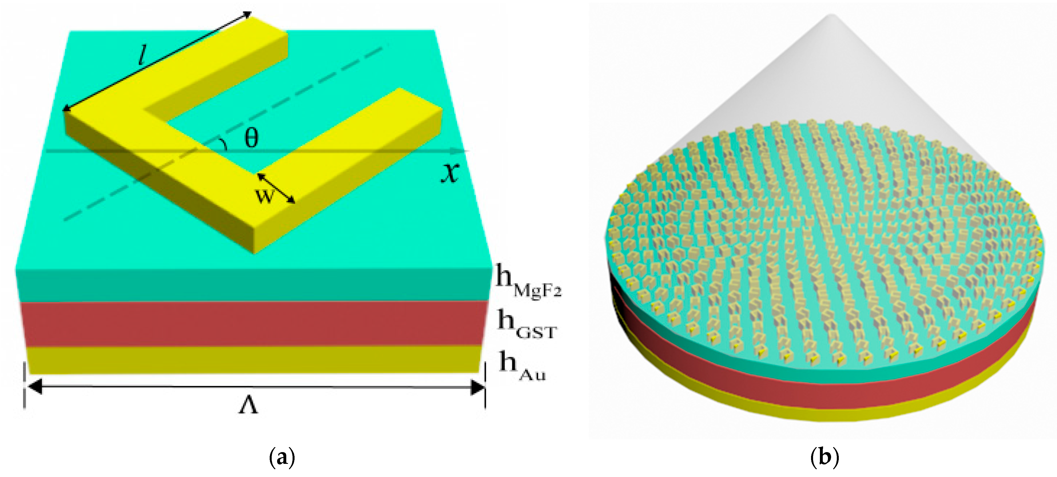
2. Fundamental and Scheme

Different from traditional volumetric metamaterials, the 2D metasurfaces are constructed of atoms with different geometries for anisotropic amplitude and phase control. Herein, the high-density U-shaped atoms with relatively large fill factor (that is defined as the ratio of resonator area to that of a periodic cell in the 2D lattice) are used in a metal-insulator-metal (MIM) architecture due to the relatively high optical efficiency in amplitude modulations, as shown in Figure 1.
At the incidence of linearly or circularly polarized (i.e., LP or CP) waves, the amplitude and phase of polarized components along different directions are tuned in an anisotropic and localized manner, as can be expressed by the Jones matrix below
[ E x o u t E y o u t ] = J [ E x i n E y i n ]
Herein, the Jones matrix JCP for CP wave incidence is
J C P = [ t L L t R L t L R t R R ]
where tLR denote the cross-polarization ratio of left circularly polarized (LCP) component to right circularly polarized (RCP) component and tRL denote that of RCP component to the LCP component, whereas tLL and tRR denote the ratios of co-polarization from LCP to LCP and RCP to RCP.
As for a local U-shaped antenna rotated by an angle θ with respect to the x-axis, shown in Figure 1a, the reflected (output) LCP and RCP component [ELCPout, ERCPout] at incidence (input) of LCP or RCP waves [ELCPin, ERCPin] can be expressed as
[ E L C P o u t E R C P o u t ] = J C P ( θ ) [ E L C P i n E R C P i n ]
where the new Jones matrix for a rotated atom can be derived by applying the rotation transformation as
J C P ( θ ) = [ t L L t R L e 2 θ t L R e 2 θ t R R ]
As a result, taking the LCP output component ELCP out as an example, namely, E L C P o u t = E L C P i n t L L + E R C P i n t L L e 2 θ by Equations (3) and (4), the first term denotes the co-polarized part whereas the second term denotes the cross-polarized part. Obviously, the latter indicates an extra phase variation of Φ = −2θ for RCP-to-LCP cross-polarization. Similarly, the extra phase shift for LCP-to-RCP cross-polarization is Φ = 2θ. Therefore, any local phase distribution can be reshaped by the meta-atoms array in a pixel-wise and sub-wavelength manner.
Further, to construct a reflective meta-lens based on the MIM architecture in Figure 1a, the parabolic phase profile needs to be constructed in the (x, y) plane, namely,
Φ ( x , y ) = ± k 0 ( x 2 + y 2 + f 2 | f | )
where k0 = 2π/λ is the free-space wave vector, f is the focal length as-designed. Therefore, ultimate surface layout for lensing is constructed by encoding the phase distributions in Equation (5) into the spatially distributed U-shaped antenna with varied angles by Φ = 2θ, as shown in Figure 1b.
As a result, the proposed MIM-based device works in a Fabry-Pérot resonant mode and provides the maximized cross-polarization to produce phase profile as-designed by Equation (5) for a given wavelength range when the sandwiched Ge2Sb2Te5 film is in the amorphous state. On the contrary, when the Ge2Sb2Te5 film undergoes a phase change to crystalline state, the cross-polarization for geometric phase generation is minimized or switched off to leave only the co-polarized component for normal specular reflection in the same wavelength range. Namely, such MIM-based meta-lens provides a photonic switch that works between “on” and “off” states for switchable lensing.
Herein, the Ge2Sb2Te5 phase change occurs at possible excitations of thermal heating, electrical stimuli or laser pulses. Essentially, the MIM setup of meta-atom design combines the advantages of reflective focusing with high optical efficiency and utility for phase transition of Ge2Sb2Te5. In special, as is recently confirmed for the similar MIM setup [41], thermal heating only triggers the one-way amorphous-to-crystalline phase change due to high temperature (above the melting point of underneath Cu) for reamorphization. Therefore, laser pulses or electrical stimuli can be introduced by proper optoelectronic design, e.g., electrical excitations in the well-known framework of phase-change memory for further compact device integration. In particular, the electrical heating by indium tin oxide (ITO) microheaters turns out to be a viable way for electrically active control, in which the diffusion barrier usually needs to be involved for practical device fabrication and long-term stability [38].

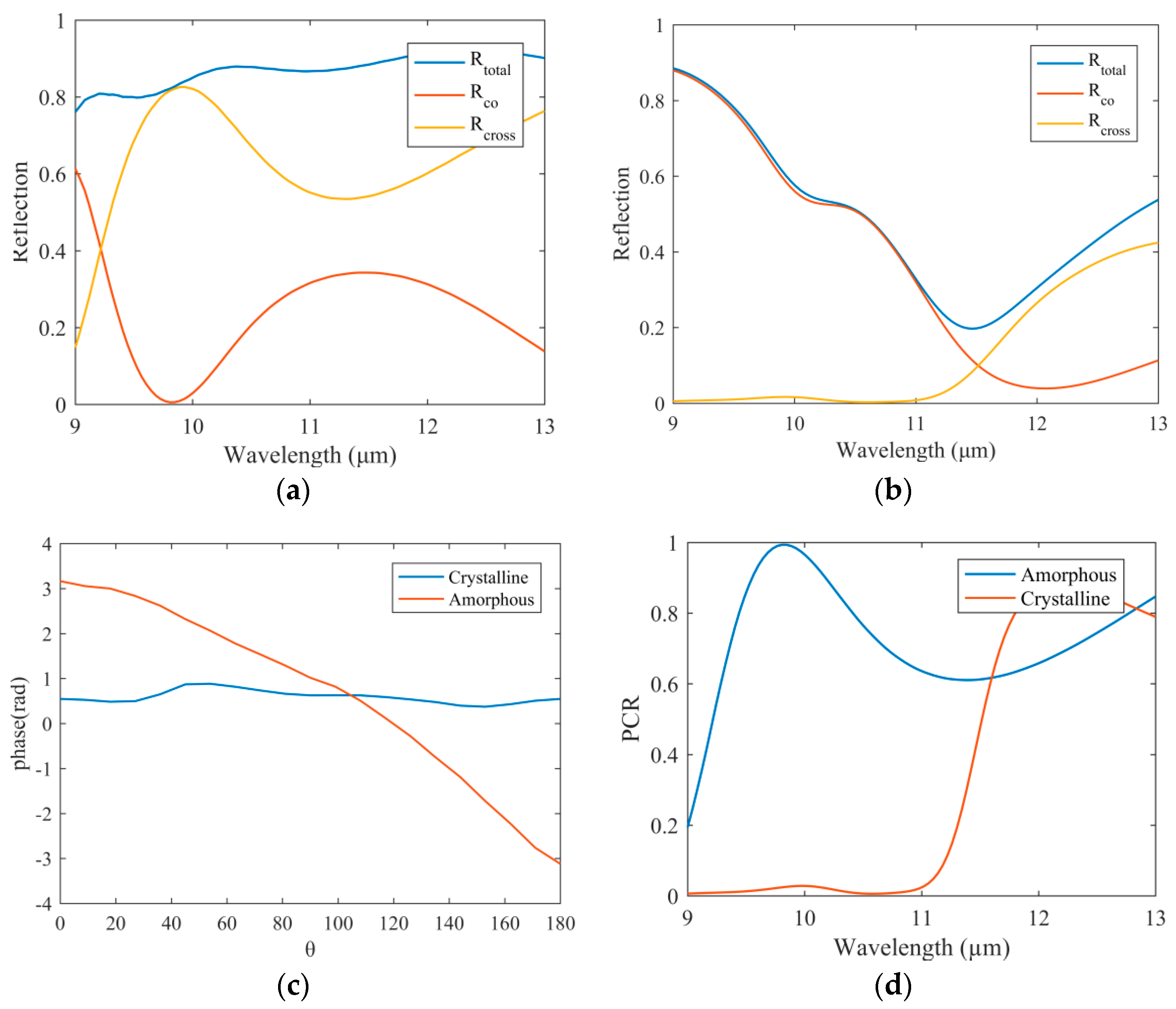
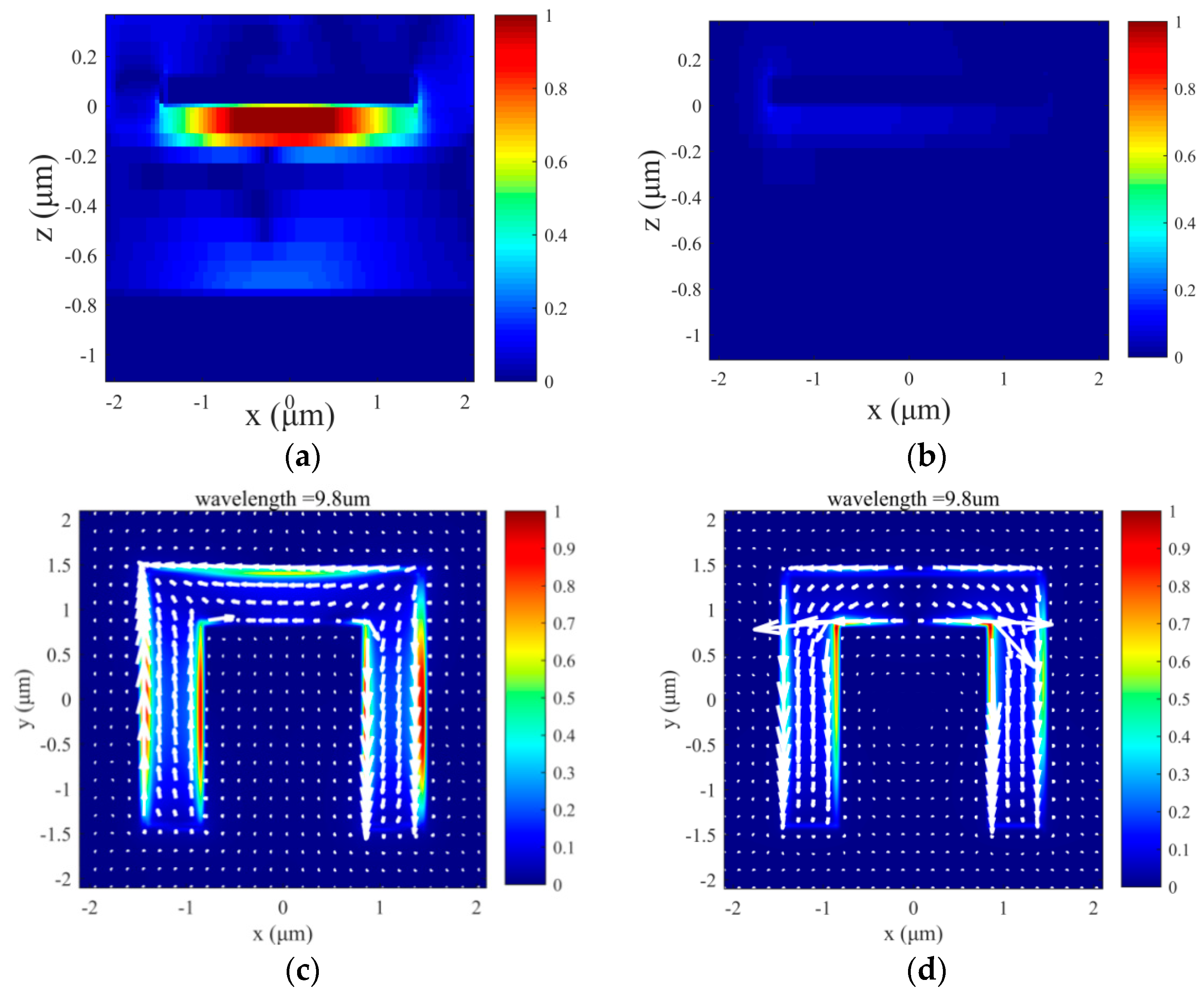
3. Simulations and Verifications

As a proof of concept, the meta-atom model is designed as in Figure 1 and numerically simulated using the finite difference time domain (FDTD) method to confirm the switchable meta-lensing at normal incidence of RCP waves. For the MIM structure in Figure 1a, the antenna parameters are set to be l = 2.88 µm and w = 0.6 µm with the thickness of 0.12 µm.
Here, the Ge2Sb2Te5 film should be adequately thick to cause appreciable spectral shift to switch off the resonance and cross-polarization at given wavelength range upon phase transition, but not too thick for reversible triggering by possible optical or electrical pulses. Therefore, also confirmed by recent studies using the similar MIM setup [1,40], the Ge2Sb2Te5 film thickness is chosen as 0.6 µm for reversible phase change under electrical or optical stimuli and enough for photonic switching, and hMgF2 = 0.15 µm and hAu = 0.12 µm, and the atom pitch is Λ = 4.2 µm, shown in Figure 1a. Optical constant of Ge2Sb2Te5 is cited from previous work [40,41]. After calculations, the reflectance of co-polarized and cross-polarized components and total reflected waves are extracted.
As shown in Figure 2a, for amorphous state of Ge2Sb2Te5, the cross-polarized reflectance (close to 80%) is maximized and becomes dominant over that of co-polarization (less than 10%) in total components of reflected waves in a broad range between 9.5~10.5 µm (around the resonance wavelength at 9.8 µm), whereas for the crystallized Ge2Sb2Te5 (Figure 2b) after amorphous-to-crystalline phase change, the cross-polarized reflectance of this device is then suppressed close to zero, and the co-polarized component becomes maximized to almost equals to the total reflection. Obviously, the cross-polarized reflectance between two states of Ge2Sb2Te5 assumes an ultra-high contrast.
Considering cross-polarized component further contributing to as-designed meta-lensing for amorphous state of Ge2Sb2Te5, the contrast of focused intensity is even higher. Therefore, such ultrahigh contrast ratio of reflectance enables a sensitive lensing switch for bistable active control. For the geometric phase produced by U-shaped antenna, shown in Figure 2c, the continuous rotation angle from zero to 180 degree produces the spatially distributed phase variations covering a full range of [0 2π].
Further, to characterize the cross-polarization efficiency for geometric phase, the polarization conversion ratio (PCR) is defined as cross-polarized reflectance over total reflection, namely, PCR = Rcross/(Rcross + Rco). Similarly, PCR spectrum extracted in Figure 2d also assumes an obvious high contrast between the amorphous and crystalline states of Ge2Sb2Te5 in the chosen range of range 9.5~10.5 µm. In particular, at the resonance point of 9.8 µm, the largest PCR contrast ratio attains to be 98% versus 2.7% (~36:1).
To illustrate the resonance mechanism of F-P mode and U-shaped antenna for switchable cross-polarization, the electric field intensity distributions are extracted in Figure 3. Clearly, at the RCP incidence of λ = 9.8 µm for the amorphous Ge2Sb2Te5 (Figure 3a), the intensity profile indicates highly confined E-field by resonant meta-atom of antenna leading to the maximized cross-polarization for as-designed geometric phase. However, crystallization of Ge2Sb2Te5 (Figure 3b) leads to almost no E-field confinement or resonance and thus minimized cross-polarization with no geometric phase. Further, at the incidence of x- and y-polarized wave at λ = 9.8 µm for amorphous Ge2Sb2Te5, the electric displacement profiles in Figure 3c,d also reveal the symmetric and asymmetric modes of resonant U-shaped antenna leading to high cross-polarization or PCR (~98%).
As a result, FDTD calculations of the whole meta-device designed in Figure 1b give rise to switchable focusing in two states of Ge2Sb2Te5. As shown in Figure 4, at three wavelengths of 10 µm, 10.5 µm, and 11 µm selected from the spectral range with high PCR contrast in Figure 2d, the extracted xoz intensity profiles obviously demonstrate the “on” and “off” states of our metalens-based photonic switch with switchable focusing. The calculated focal lengths in Figure 4a–c are 67.8 µm, 65 µm, and 60.7 µm, which agrees well with both Equation (5) and the generalized Snell’s law, since larger wavelengths lead to smaller deflection angles as well as smaller focal lengths.

4. Conclusions

In conclusion, to address the issue of passive nature and low optical efficiency that exists in most of current metasurface devices, one type of PCM-based planar meta-lens is proposed and numerically verified with actively switchable focusing by integrating the U-shaped meta-atoms and chalcogenide alloy of Ge2Sb2Te5 into the reflective MIM architecture. By distributing the U-shaped antenna array with intrinsically high fill factor pixel-wise, the phase profile can be reshaped as designed for the switchable lensing with high optical efficiency and ultrahigh contrast ratio up to 36:1. The switchable behavior occurs upon a conditional phase transition of Ge2Sb2Te5 between the amorphous and crystalline states, which can be optically or electrically triggered in practical device integration, e.g., based on the previously reported MIM architecture [1,41]. At the amorphous state of the embedded Ge2Sb2Te5 layer, the reflected cross-polarized component is maximized (i.e., switched “on”) for the as-designed geometric phase to define the normal focusing, or minimized (switched “off”) with no focusing when the Ge2Sb2Te5 layer is switched to a crystalline state. As a result, our scheme potentially paves a promising way to construct the metasurface-based active photonic devices, especially for ultracompact integration.

Author Contributions

Conceptualization, X.M., R.S. and S.Z.; data curation, Z.F. and R.S.; methodology, Z.F., R.S., X.M. and S.Z.; software, Z.F. and R.S.; writing—original draft preparation, X.M., Z.F. and S.Z.; writing—review and editing, Z.F., R.S. and S.Z. All authors have read and agreed to the published version of the manuscript.

Funding

This research was funded by the Chongqing Science Foundation for Distinguished Young Scholars (Grant No. cstc2020jcyj-jqX0019), and the Provincial Natural Science Foundation of Guangdong.

Institutional Review Board Statement

Not applicable.

Informed Consent Statement

Not applicable.

Data Availability Statement

Not applicable.

Conflicts of Interest

The authors declare no conflict of interest.

References

  1. Ruirui, S.; Qinling, D.; Shaolin, Z.; Mingbo, P. Catenary-based phase change metasurfaces for mid-infrared switchable wavefront control. Opt. Express 2021, 29, 23006–23018. [Google Scholar] [CrossRef]
  2. Hail, C.U.; Michel, A.K.U.; Poulikakos, D.; Eghlidi, H. Optical Metasurfaces: Evolving from Passive to Adaptive. Adv. Opt. Mater. 2019, 7, 1801786. [Google Scholar] [CrossRef]
  3. Zhihua, F.; Qinling, D.; Xiaoyu, M.; Shaolin, Z. Phase change metasurfaces by continuous or quasi-continuous atoms for active optoelectronic integration. Materials 2021, 14, 1272. [Google Scholar] [CrossRef]
  4. Zhou, S.; Mu, S.; Raju, S.; Prawoto, C.; Ruan, X.; Ng, K.; Chan, M. Prototyping of Terahertz Metasurface by One-Step Lithographically Defined Templating. IEEE Photonics Technol. Lett. 2018, 30, 971–974. [Google Scholar] [CrossRef]
  5. Luo, X. Subwavelength Optical Engineering with Metasurface Waves. Adv. Opt. Mater. 2018, 6, 1701201. [Google Scholar] [CrossRef]
  6. Zhou, F.; Qin, F.; Yi, Z.; Yao, W.; Liu, Z.; Wu, X.; Wu, P. Ultra-wideband and wide-angle perfect solar energy absorber based on Ti nanorings surface plasmon resonance. Phys. Chem. Chem. Phys. 2021, 23, 17041–17048. [Google Scholar] [CrossRef]
  7. Yoo, S.J.; Park, Q.H. Metamaterials and chiral sensing: A review of fundamentals and applications. Nanophotonics 2019, 8, 249–261. [Google Scholar] [CrossRef] [Green Version]
  8. Zhao, Y.; Wang, L.; Zhang, Y.; Qiao, S.; Liang, S.; Zhou, T.; Zhang, X.; Guo, X.; Feng, Z.; Lan, F.; et al. High-Speed Efficient Terahertz Modulation Based on Tunable Collective-Individual State Conversion within an Active 3 nm Two-Dimensional Electron Gas Metasurface. Nano Lett. 2019, 19, 7588–7597. [Google Scholar] [CrossRef]
  9. Yu, N.; Genevet, P.; Kats, M.A.; Aieta, F.; Tetienne, J.P.; Capasso, F.; Gaburro, Z. Light propagation with phase discontinuities: Generalized laws of reflection and refraction. Science 2011, 334, 333–337. [Google Scholar] [CrossRef] [Green Version]
  10. Zhou, S.; Wu, Y.; Chen, S.; Liao, S.; Zhang, H.; Xie, C.; Chan, M. Phase change induced active metasurface devices for dynamic wavefront control. J. Phys. D Appl. Phys. 2020, 53, 204001. [Google Scholar] [CrossRef]
  11. Zheludev, N.I.; Kivshar, Y.S. From metamaterials to metadevices. Nat. Mater. 2012, 11, 917–924. [Google Scholar] [CrossRef] [PubMed]
  12. Wang, S.; Wu, P.C.; Su, V.C.; Lai, Y.C.; Chen, M.K.; Kuo, H.Y.; Chen, B.H.; Chen, Y.H.; Huang, T.T.; Wang, J.H.; et al. A broadband achromatic metalens in the visible. Nat. Nanotechnol. 2018, 13, 227–232. [Google Scholar] [CrossRef] [PubMed]
  13. Huang, Y.; Pu, M.; Zhang, F.; Luo, J.; Li, X.; Ma, X.; Luo, X. Broadband Functional Metasurfaces: Achieving Nonlinear Phase Generation toward Achromatic Surface Cloaking and Lensing. Adv. Opt. Mater. 2019, 7, 1801480. [Google Scholar] [CrossRef]
  14. Dou, K.H.; Xie, X.; Pu, M.B.; Li, X.; Ma, X.L.; Wang, C.T.; Luo, X.G. Off-axis multi-wavelength dispersion controlling metalens for multi-color imaging. Opto-Electron. Adv. 2020, 3, 1–7. [Google Scholar] [CrossRef] [Green Version]
  15. Ma, X.L.; Pu, M.B.; Li, X.; Guo, Y.H.; Luo, X.G. All-metallic wide-angle metasurfaces for multifunctional polarization manipulation. Opto-Electron. Adv. 2019, 2, 180023. [Google Scholar] [CrossRef] [Green Version]
  16. Zheng, G.; Mühlenbernd, H.; Kenney, M.; Li, G.; Zentgraf, T.; Zhang, S. Metasurface holograms reaching 80% efficiency. Nat. Nanotechnol. 2015, 10, 308–312. [Google Scholar] [CrossRef]
  17. Wen, D.; Yue, F.; Li, G.; Zheng, G.; Chan, K.; Chen, S.; Chen, M.; Li, K.F.; Wong, P.W.H.; Cheah, K.W.; et al. Helicity multiplexed broadband metasurface holograms. Nat. Commun. 2015, 6, 8241. [Google Scholar] [CrossRef] [PubMed]
  18. Wang, E.; Shi, L.; Niu, J.; Hua, Y.; Li, H.; Zhu, X.; Xie, C.; Ye, T. Multichannel Spatially Nonhomogeneous Focused Vector Vortex Beams for Quantum Experiments. Adv. Opt. Mater. 2019, 7, 1801415. [Google Scholar] [CrossRef]
  19. Pu, M.; Li, X.; Ma, X.; Wang, Y.; Zhao, Z.; Wang, C.; Hu, C.; Gao, P.; Huang, C.; Ren, H.; et al. Catenary optics for achromatic generation of perfect optical angular momentum. Sci. Adv. 2015, 1, e1500396. [Google Scholar] [CrossRef] [Green Version]
  20. Cong, L.; Pitchappa, P.; Lee, C.; Singh, R. Active Phase Transition via Loss Engineering in a Terahertz MEMS Metamaterial. Adv. Mater. 2017, 29, 1700733. [Google Scholar] [CrossRef] [PubMed]
  21. Buchnev, O.; Podoliak, N.; Kaczmarek, M.; Zheludev, N.I.; Fedotov, V.A. Electrically Controlled Nanostructured Metasurface Loaded with Liquid Crystal: Toward Multifunctional Photonic Switch. Adv. Opt. Mater. 2015, 3, 674–679. [Google Scholar] [CrossRef] [Green Version]
  22. Chen, H.-T.; Padilla, W.J.; Zide, J.M.O.; Gossard, A.C.; Taylor, A.J.; Averitt, R.D. Active terahertz metamaterial devices. Nature 2006, 444, 597–600. [Google Scholar] [CrossRef] [Green Version]
  23. Low, T.; Avouris, P. Graphene plasmonics for terahertz to mid-infrared applications. ACS Nano 2014, 8, 1086–1101. [Google Scholar] [CrossRef] [Green Version]
  24. Park, J.; Kang, J.H.; Kim, S.J.; Liu, X.; Brongersma, M.L. Dynamic reflection phase and polarization control in metasurfaces. Nano Lett. 2017, 17, 407–413. [Google Scholar] [CrossRef]
  25. Wuttig, M.; Bhaskaran, H.; Taubner, T. Phase-change materials for non-volatile photonic applications. Nat. Photonics 2017, 11, 465–476. [Google Scholar] [CrossRef]
  26. Gholipour, B.; Zhang, J.; MacDonald, K.F.; Hewak, D.W.; Zheludev, N.I. An all-optical, non-volatile, bidirectional, phase-change meta-switch. Adv. Mater. 2013, 25, 3050–3054. [Google Scholar] [CrossRef] [PubMed]
  27. Raeis-Hosseini, N.; Rho, J. Metasurfaces based on phase-change material as a reconfigurable platform for multifunctional devices. Materials 2017, 10, 1046. [Google Scholar] [CrossRef] [PubMed] [Green Version]
  28. Cui, T.; Bai, B.; Sun, H.B. Tunable Metasurfaces Based on Active Materials. Adv. Funct. Mater. 2019, 29, 1806692. [Google Scholar] [CrossRef]
  29. Kang, L.; Jenkins, R.P.; Werner, D.H. Recent Progress in Active Optical Metasurfaces. Adv. Opt. Mater. 2019, 7, 1801813. [Google Scholar] [CrossRef] [Green Version]
  30. Guo, P.; Lombardo, D.; Sarangan, A. Vanadium dioxide switchable components based on wiregrids for mid-infrared applications. In Proceedings of the Nanoengineering: Fabrication, Properties, Optics, and Devices XIV, San Diego, CA, USA, 30–31 August 2016; Campo, E.M., Dobisz, E.A., Eldada, L.A., Eds.; SPIE: Bellingham, WA, USA, 2017; Volume 10354, pp. 161–166. [Google Scholar]
  31. Simandan, I.D.; Sava, F.; Buruiana, A.T.; Galca, A.C.; Becherescu, N.; Burducea, I.; Mihai, C.; Velea, A. Influence of deposition method on the structural and optical properties of ge2 sb2 te5. Materials 2021, 14, 3663. [Google Scholar] [CrossRef] [PubMed]
  32. Zhou, S.; Li, K.; Chen, Y.; Liao, S.; Zhang, H.; Chan, M. Phase Change Memory Cell with Reconfigured Electrode for Lower RESET Voltage. IEEE J. Electron Devices Soc. 2019, 7, 1072–1079. [Google Scholar] [CrossRef]
  33. Wuttig, M.; Yamada, N. Phase-change materials for rewriteable data storage. Nat. Mater. 2007, 6, 824–832. [Google Scholar] [CrossRef] [PubMed]
  34. Raoux, S.; Xiong, F.; Wuttig, M.; Pop, E. Phase change materials and phase change memory. MRS Bull. 2014, 39, 703–710. [Google Scholar] [CrossRef] [Green Version]
  35. Wong, H.S.P.; Raoux, S.; Kim, S.; Liang, J.; Reifenberg, J.P.; Rajendran, B.; Asheghi, M.; Goodson, K.E. Phase Change Memory. Proc. IEEE 2010, 98, 2201–2227. [Google Scholar] [CrossRef]
  36. Guo, Y.; Yan, L.; Pan, W.; Shao, L. Scattering engineering in continuously shaped metasurface: An approach for electromagnetic illusion. Sci. Rep. 2016, 6, 30154. [Google Scholar] [CrossRef] [Green Version]
  37. Taghinejad, H.; Abdollahramezani, S.; Eftekhar, A.A.; Fan, T.; Hosseinnia, A.H.; Hemmatyar, O.; Eshaghian Dorche, A.; Gallmon, A.; Adibi, A. ITO-based microheaters for reversible multi-stage switching of phase-change materials: Towards miniaturized beyond-binary reconfigurable integrated photonics. Opt. Express 2021, 29, 20449. [Google Scholar] [CrossRef]
  38. Schlich, F.F.; Zalden, P.; Lindenberg, A.M.; Spolenak, R. Color switching with enhanced optical contrast in ultrathin phase-change materials and semiconductors induced by femtosecond laser pulses. ACS Photonics 2015, 2, 178–182. [Google Scholar] [CrossRef]
  39. Yoo, S.; Gwon, T.; Eom, T.; Kim, S.; Hwang, C.S. Multicolor Changeable Optical Coating by Adopting Multiple Layers of Ultrathin Phase Change Material Film. ACS Photonics 2016, 3, 1265–1270. [Google Scholar] [CrossRef]
  40. Zhang, M.; Pu, M.; Zhang, F.; Guo, Y.; He, Q.; Ma, X.; Huang, Y.; Li, X.; Yu, H.; Luo, X. Plasmonic Metasurfaces for Switchable Photonic Spin–Orbit Interactions Based on Phase Change Materials. Adv. Sci. 2018, 5, 1800835. [Google Scholar] [CrossRef]
  41. Zhou, S.; Chen, S.; Wu, Y.; Liao, S.; Li, H.; Xie, C.; Chan, M. Bistable active spectral tuning of one-dimensional nanophotonic crystal by phase change. Opt. Express 2020, 28, 8341. [Google Scholar] [CrossRef]
Figure 1. (a) The U-shaped atoms with rotated angle of θ to x-axis and (b) meta-surface lens by locally distributing all atoms with different angles.
Coatings 11 01499 g001
Figure 2. The total, co-polarized, and cross-polarized components of reflection for (a) amorphous and (b) crystalline states of GST layers. (c) The phase shift versus varied rotation angles of the U-shaped antenna and (d) the PCR spectrum before and after the amorphous-to-crystalline phase transition.
Coatings 11 01499 g002
Figure 3. The calculated electric field intensity profile of U-shaped antenna incident by RCP wave at with the resonant wavelength λ = 9.8 µm for (a) amorphous and (b) crystalline states of Ge2Sb2Te5; (c,d) the electric displacement profile under LP waves along the (c) x (symmetric) and (d) y (asymmetric) directions.
Coatings 11 01499 g003
Figure 4. The amplitude profiles for amorphous-GST at the incident wavelengths of (a) 10 μm (b) 10.5 μm and (c) 11 μm with obvious focusing; after GST phase change into the crystalline state, the amplitude profiles for crystalline-GST at the wavelengths of (d) 10 μm, (e) 10.5 μm, and (f) 11 μm indicate no focusing.
Coatings 11 01499 g004
Publisher’s Note: MDPI stays neutral with regard to jurisdictional claims in published maps and institutional affiliations.

