Review

Recent Studies on the Fabrication of Multilayer Films by Magnetron Sputtering and Their Irradiation Behaviors

1
School of Materials Science and Engineering, Harbin Institute of Technology, Shenzhen 518055, China
2
Institute of Special Environments Physical Sciences, Harbin Institute of Technology, Shenzhen 518055, China
*
Authors to whom correspondence should be addressed.
Coatings 2021, 11(12), 1468; https://doi.org/10.3390/coatings11121468
Submission received: 30 October 2021 / Revised: 21 November 2021 / Accepted: 22 November 2021 / Published: 29 November 2021
(This article belongs to the Special Issue Nanocomposite Thin Film and Multilayers)

Abstract

:
Multilayer films with high-density layer interfaces have been studied widely because of the unique mechanical and functional properties. Magnetron sputtering is widely chosen to fabricate multilayer films because of the convenience in controlling the microstructure. Essentially, the properties of multilayer films are decided by the microstructure, which could be adjusted by manipulating the deposition parameters, such as deposition temperature, rate, bias, and target–substrate distance, during the sputter process. In this review, the influences of the deposition parameters on the microstructure evolution of the multilayer films have been summarized. Additionally, the impacts of individual layer thickness on the microstructure evolution as well as the irradiation behavior of various multilayer films have been discussed.

1. Introduction

Due to their unique structures with high-density interfaces, multilayer films have many advanced properties. For example, they are able to maintain high mechanical stability in extreme environments, such as severe tribological conditions with high temperatures [1] and energetic particle irradiation [2,3,4]. W. L. Chen et al. described the high hardness and low friction coefficient of CrAlN/TiAlSiN multilayer films [1]. E. G. Fu et al. demonstrated that Cu/V interfaces effectively reduced the concentration of radiation-induced point defects [5]. In addition, multilayer films have been widely studied for various functional applications, such as hydrogen fuel cells [6,7] and magnetic data storage [8,9]. P. Chen et al. posited that Mg/MmM5 multilayer films have good prospects for the application of hydrogen fuel cells because of their synergetic effects [7]. A. M. et al. concluded that multilayer films, such as Co/Pt and Fe/Pt, have beneficial properties for magnetic data storage [9]. This review primarily focuses on multilayer films with metallic systems whose irradiation behaviors are studied extensively.
Among numerous preparation methods, magnetron sputtering provides multiple advantages, including controllable properties, high efficiency, and favorable substrate–film bonding strength; as a result, the benefits of this method are widely exploited in the fabrication of multilayer films [10,11,12,13]. For instance, individual layer thickness, one of the most important parameters in determining the properties of multilayer films, can be readily adjusted during the sputtering process [14,15]. Moreover, this method is also suitable for preparing alloy films and compounds with different compositions [16]. During the sputtering process, multiple parameters play important roles in the microstructure evolution of multilayer films, such as the deposition temperature, rate, bias, and the target–substrate distance. The influences of some parameters have been extensively studied, such as the deposition temperature and bias, whereas other parameters, such as the deposition rate, are not well understood [17,18,19,20,21,22].
Meanwhile, the individual layer thickness also exerts great impacts on the microstructure change of multilayer films, such as the flatness of interfaces, defect density, and coherency [23,24,25,26]. When the total thickness of the multilayer films is constant, the thinner the individual layer thickness, the higher the interface density, which may significantly affect many properties of films including the irradiation tolerance. During irradiation, a large population of point defects and larger defect clusters, such as dislocation networks and voids, are introduced into materials under the bombardment of energetic particles [27,28,29,30,31,32]. Such significant microstructure damages can cause swelling, hardening, embrittlement, and other problems in materials which significantly shorten their service life [33,34]. The irradiation stability of a material can be strengthened through introducing defect sinks, such as grain boundaries (GBs) [35,36,37,38], twin boundaries (TBs) [39,40,41,42,43,44,45], and free surface [46,47,48,49,50,51,52], which facilitate the recombination of irradiation-induced defects and defect clusters. It is well known that interfaces may also act as effective defect sinks [53]. Therefore, multilayer films with high-density layer interfaces are considered as irradiation-resistant materials and have been widely investigated [54,55,56,57,58,59,60]. Additionally, multilayer films also have good mechanical properties, such as ductility, yield strength, hardness, etc., which can also be manipulated by changing the parameters during the fabrication process [61,62].
In this review, we summarize the relationships between the preparation parameters and the microstructure evolution of multilayer films. In addition, the influences of individual layer thickness on the microstructure and irradiation behavior of multilayer films are discussed. We integrate extensive research efforts into relevant fields with the goal of providing researchers with a guide to develop advanced multilayer metal films with beneficial properties in the future.

2. The Effects of Deposition Parameters on the Microstructure of Multilayer Films

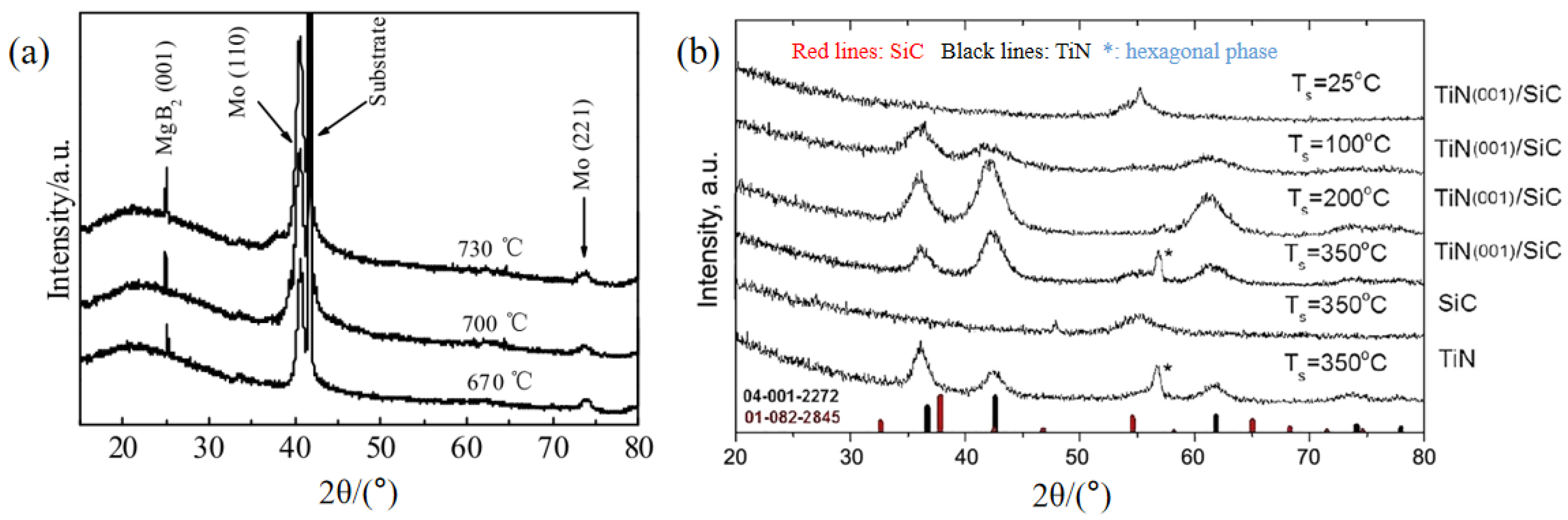
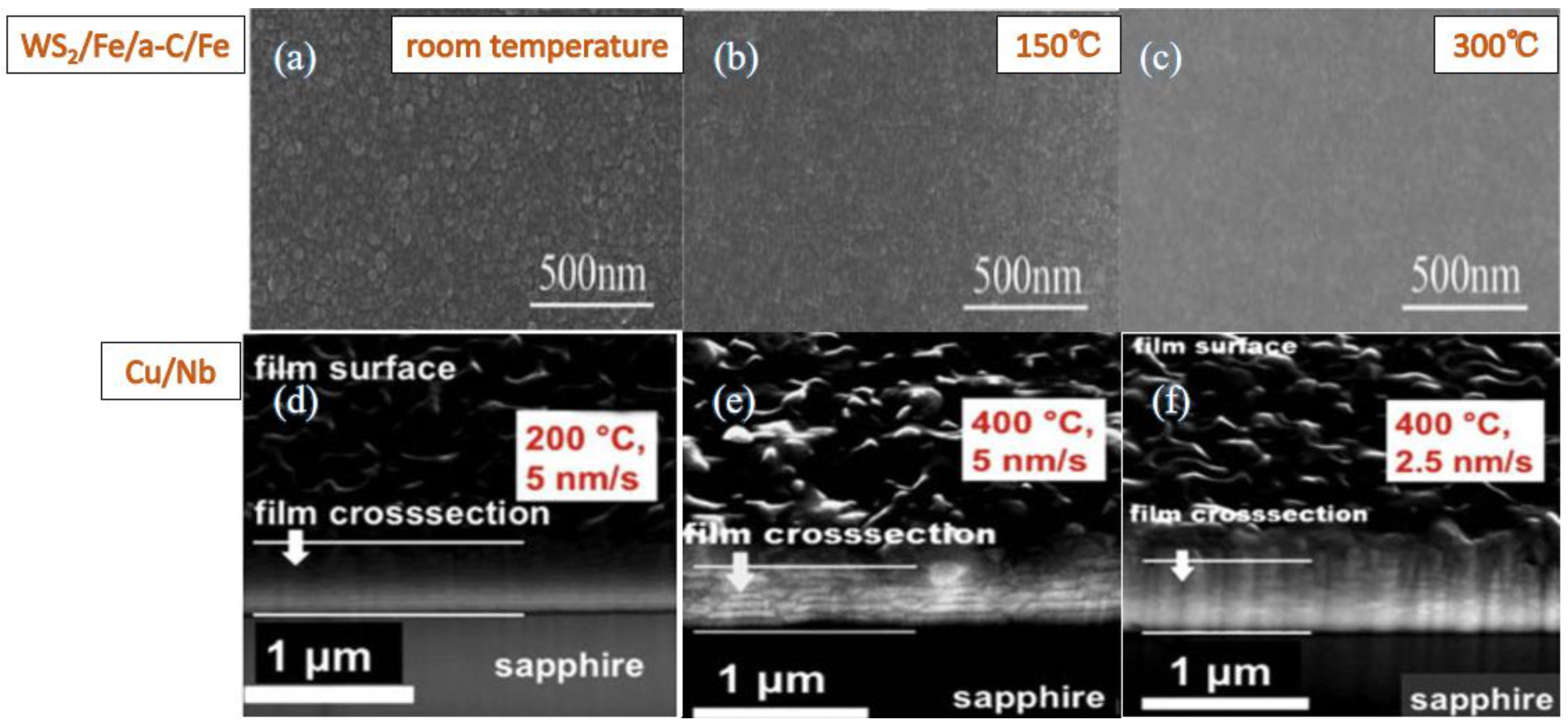
2.1. The Effect of Substrate Temperature

In principle, the microstructure and morphology of multilayer films are governed by the kinetics of the mobile adatoms on the substrate, which can be easily controlled by the substrate temperature during the sputtering process [21,63]. Therefore, the effect of substrate temperature on thin-film fabrication has been widely investigated [2,17,19,64,65]. During sputter deposition, the mobility of the adatoms, among other factors, drives the condensation, nucleation, and crystallization processes [63]. Higher substrate temperature can provide additional energy for adatoms to migrate and reconstruct into the lowest surface structure, which results in the improvement of the crystallinity, density, etc., of the films [66]. In contrast, the defect density and film roughness decrease [17,21,22]. It is also reported that increasing the substrate temperature can lead to the formation of new compounds between different components of multilayer films, thereby changing the film properties [67].
X-ray diffraction (XRD) patterns of two multilayer systems prepared at different temperatures are shown in Figure 1. Z. Zhou et al. prepared several groups of MgB2/Mo multilayer films at different temperatures. Figure 1a shows that the intensity of the Mo (110) and MgB2 (001) diffraction peaks increases with temperature. Detailed data are listed in Table 1. As the temperature increases from 670 to 730 °C, the Full Width at Half Maximum (FWHM) of the Mo (110) and MgB2 (001) diffraction peaks decreases, indicating the improvement of crystallinity. Additionally, the interplanar spacing of Mo (110) increases with the deposition temperature and eventually reaches 0.2236 nm at 730 ℃ compared to the standard value of 0.2225 nm, indicating that the residual tensile stress of the Mo layers increases with rising temperature due to the reduced defect density in the films [24].
The grazing incidence X-ray diffraction (GIXRD) patterns of TiN/SiC multilayer films deposited at a series of temperatures are shown in Figure 1b. When the deposition temperatures are 25 and 100 °C, the structure of the multilayer films consists of nanocrystalline TiN layers with small grains and amorphous silicon carbide layers. As the substrate temperature increases to 200 and 350 °C, amorphous SiC begins to crystallize. In comparison, pure SiC films are still highly amorphous at this temperature [68]. Evidently, the crystallinity of the multilayer films can be improved by increasing the temperature. However, a special case exists if the thermal energy can overcome the activation energy of defect proliferation when the deposition temperature exceeds a certain threshold, such as 600 °C for Ge/Si multilayer films. Consequently, high-density misfit dislocations are formed, which jeopardize the crystallinity of multilayer films [19].
Figure 2 shows scanning electron microscope (SEM) micrographs of two multilayer systems. The effect of substrate temperature on the microstructure of the films can be observed. As shown in Figure 2a–c, the surface of WS2/Fe/a-C/Fe multilayer films becomes smoother and denser at higher substrate temperatures. In general, a sputtered Fe layer shows a porous columnar structure; however, when deposition temperature is increased, the adatoms obtain enough energy to fill the channels between columnar grains. As a consequence, the shadow effect caused by Fe layers is mitigated, forming smoother and denser films [22].
It is worth noting that higher substrate temperature does not always produce lower film roughness. This conclusion only applies to the temperature at which the aggregation of small grains is suppressed. Otherwise, the film surface will become rougher due to the formation of large grains. T. Wu et al. experimentally demonstrated that the smoothest morphology was obtained when the substrate temperature was ~200 °C for Au/NiCr/Ta multilayer films. Further increasing the temperature caused a rougher film surface [17].
Figure 2d,f present the effect of deposition temperature on the microstructure change of Cu/Nb multilayer films. The morphology of the film surface shows larger grains at higher deposition temperatures. The cross-sections of the films show that the multilayer films deposited at 200 °C have better continuity in their layers than those at 400 °C. This is because the energy of adatoms decreases at a lower temperature and fewer Cu atoms can diffuse to the adjacent Nb layers, resulting in much fewer pinch-off events [2].
Increasing the substrate temperature can also change the composition of multilayer films, such as Ni/Al multilayer films. Previous studies have shown that L12-ordered Ni3Al can be obtained in Ni/Al multilayer films either by post-annealing or by increasing the substrate temperature during fabrication [67]. This phenomenon can change the irradiation behavior of the films.
In conclusion, manipulating the substrate temperature can change the crystallinity, density, composition, surface roughness, etc. In general, raising the substrate temperature can increase the grain size, improve the crystallinity and density of multilayer films, and reduce defect density and surface roughness. However, high deposition temperature may also lead to the formation of high-density misfit dislocations, thereby reducing the crystallinity and surface flatness. In addition, new compounds may form in some multilayer systems with miscible interfaces and negative heat of mixing when sufficient heat is provided.

2.2. The Effect of Deposition Rate

The deposition rate is not an independent parameter that can be directly controlled in the sputtering process. In general, the deposition rate can be adjusted by manipulating other parameters, such as deposition power (sputtering power), gas pressure, or target–substrate distance [69]. The deposition power, among other parameters, is frequently chosen to adjust the rate [53]. Table 2 shows the FWHM and the signal-to-noise ratio (SNR) of XRD curves of Cu/Nb multilayer films deposited at different substrate temperatures with different deposition rates of Cu. Several selected SEM micrographs are shown in Figure 2d–f. In this case, slower deposition rates could give the adatoms enough time to migrate and arrange according to the normal lattice structure. As a result, the defect density in Cu decreases and also leads to a decreased defect density in the adjacent Nb layers. Consequently, the crystallinity of the multilayer films is promoted [2]. However, decreasing the deposition rate also enhances the probability that Cu atoms will migrate between adjacent layers, which adversely affects the layer continuities, as shown in Figure 2e,f [2].
Many previous studies have reported that the deposition rate can be easily controlled by the deposition power and higher deposition power normally leads to a faster deposition rate. However, it is worth mentioning that high power may also introduce a high degree of ionization, high plasma density, and hence high ion flux towards the substrate, which will eventually affect the microstructure and morphology of the films [70]. Clearly, the effects of the deposition rate on the microstructures of multilayer films need further investigation.

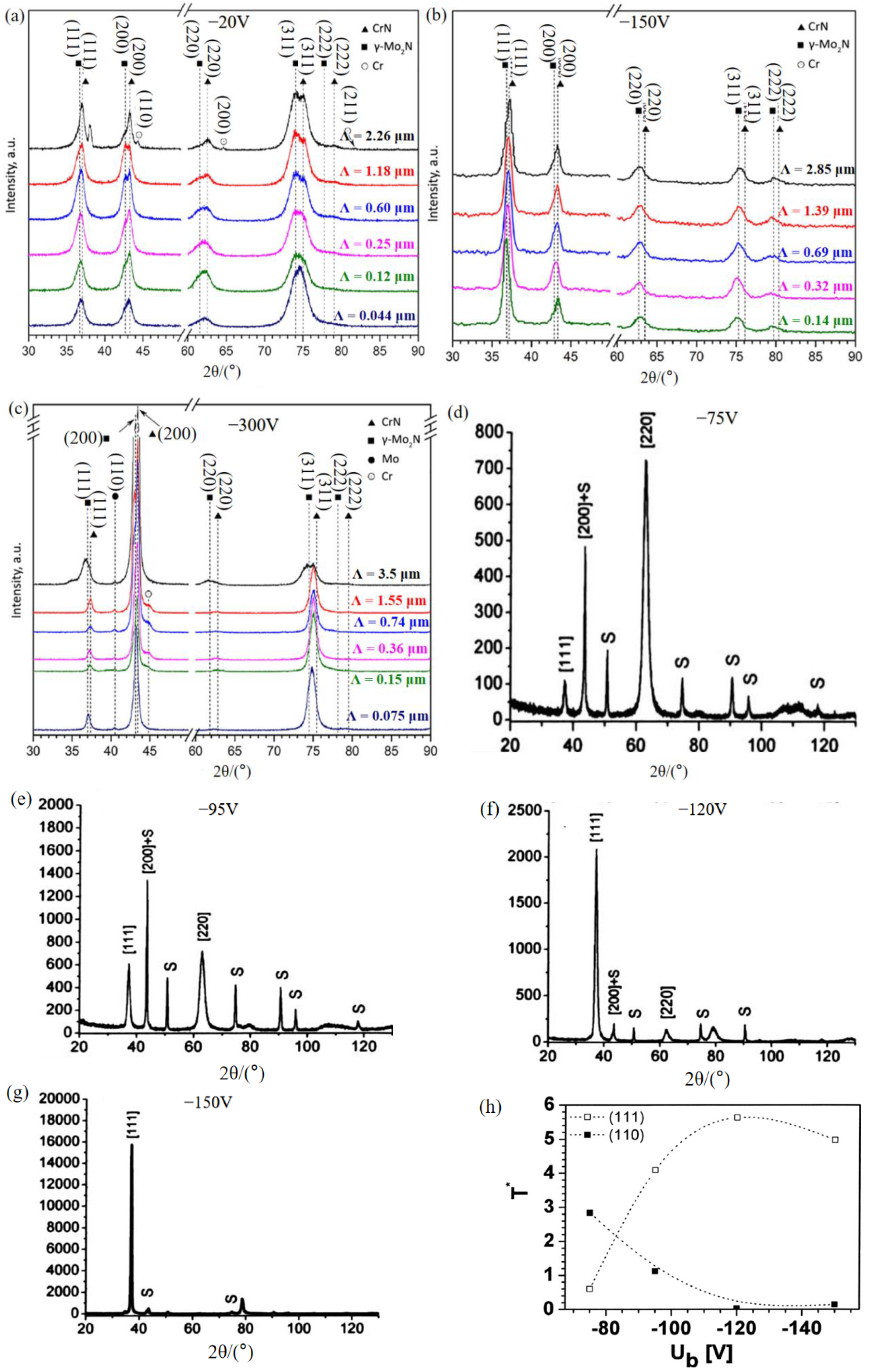
2.3. The Effect of Deposition Bias

The bias voltage is another important parameter in the sputtering process. Increasing the bias will increase the energy of the sputtered particles [20]. As a consequence, the adatoms possess higher energy, affecting the microstructure and morphology of the multilayer films [71]. The XRD curves of CrN/MoN multilayer films deposited at different biases are shown in Figure 3a–c. The results indicate that the texture of the films can be altered by changing the deposition bias. For instance, the films exhibit strong (311) texture when the applied bias Ub = −20 V. As Ub increases to −150 V, solid solution (Cr, Mo) N forms at the interfaces between the layers, resulting in predominantly (111) texture, as shown in Figure 3b. When Ub is further increased to −300 V, the content of N decreases, leading to the preferred formation of the (200) texture [72].
The texture changes of CrAlYN/CrN multilayer films grown on a CrAlN base layer and prepared under different biases are shown in Figure 3d–h and Figure 4a–d. With the increase in bias voltage, the preferred texture gradually evolves from a mixture of (220) and (222) textures to a predominant (111) texture. The texture evolution is summarized in Figure 3h. It is evident that as the bias increases, the intensity of (110) texture gradually declines, while the intensity of the (111) texture is gradually enhanced. When the bias is above −120 V, the films exhibit primarily (111) texture. The texture evolution is mainly attributed to the increased internal stress in the films at a larger bias because the CrAlYN/CrN multilayer films exhibit a face-centered cubic (FCC) structure and the (111) texture is preferred under greater stress [20].
The TEM micrographs and corresponding SAED patterns in Figure 4 show the microstructure change of CrAlYN/CrN multilayer systems with different biases. In addition to the change in texture, because the energy of sputtered particles increases with a rise in bias, different microscopic morphologies are formed. When the bias voltage is −75 V, as shown in Figure 4a, both the base layer (CrAlN) and the above multilayers are polycrystalline with columnar grains. When the bias voltage increases to −95 V, the density of the layers increases due to the enhanced energy of the sputtered particles. As can be observed in Figure 4b, the size of the columnar grains and the density both increase. As the base layer contains both columnar and large single-crystal domains with a strongly pronounced local epitaxial growth on the substrate, the base layer forms a single-crystal structure under the bombardment of high-energy adatoms as the bias voltage increases to −120 V, whereas the multilayer structure remains polycrystalline. When the bias voltage increases to −150 V, a single-crystal structure is present in both the base layer and the multilayers [20].
In conclusion, manipulating the bias can change the stress, density, composition, texture orientation, crystallinity, crystal structure, etc. In general, as the bias increases, the stress in the multilayer films rises, thereby improving the crystallinity and density, and the texture is prone to change into the orientation with lower energy. The composition can also be changed with different biases, which will also affect the texture of the films.

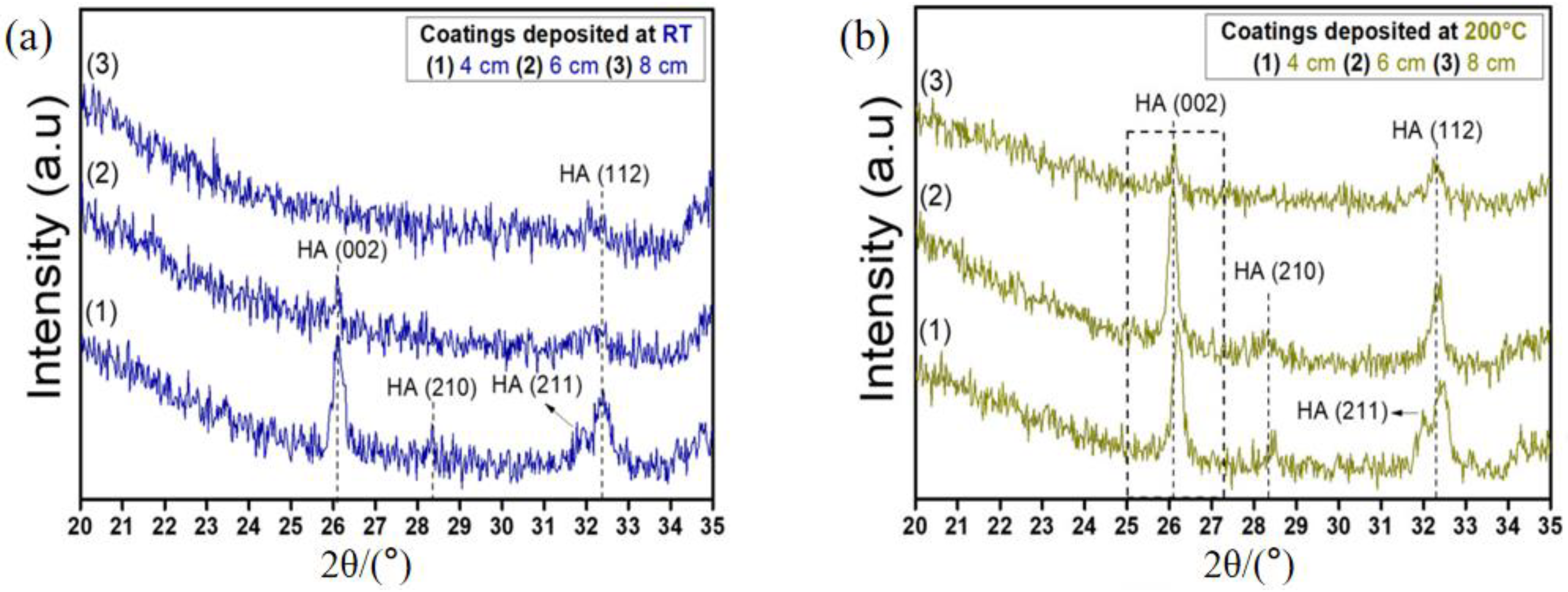
2.4. The Effect of Target–Substrate Distance

The target–substrate distance is another parameter that can be manipulated to modify the microstructure of multilayer films in the sputtering process. In general, shortening the target–substrate distance will increase the energy of adatoms, thereby altering the crystallinity, density, and other properties of the multilayer films. Notably, shortening the target–substrate distance can promote the sputtering rate but also decrease the uniformity of the films [73]. Therefore, an appropriate target–substrate distance is important during the film fabrication process.
In many cases, the crystallinity of the films is determined by the energy of the adatoms [67]. Figure 5 shows hydroxyapatite (HA)/Ag multilayer films prepared at different target–substrate distances and temperatures. As is clearly shown in Figure 5a,b, the shorter the target–substrate distance, the sharper the XRD diffraction peak, indicating better crystallinity of the films. When the target–substrate distance decreases from 8 to 4 cm, sputtered particles have a lower probability of colliding and decelerating, and the adatoms retain higher energy, resulting in a higher crystallinity of the multilayer films. Table 3 shows the crystallite size of HA/Ag multilayer films prepared at different substrate temperatures and target–substrate distances. Shorter target–substrate distances result in a higher energy of the adatoms, leading to the formation of larger grains. When the target–substrate distance reaches 8 cm, the amorphous structure can even be produced at room temperature [18].

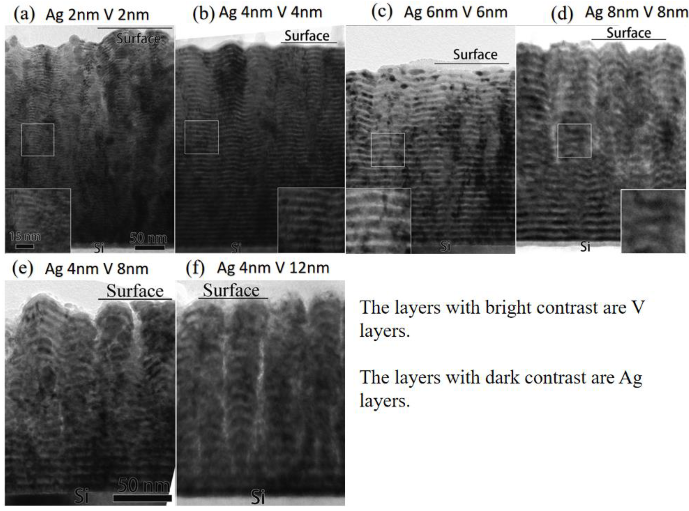
3. The Effect of Layer Thickness on the Microstructures of Multilayer Films

The layer thickness of the multilayer films discussed in this review refers to the thickness of the individual layer. It normally exerts great influence on various properties and irradiation behaviors of multilayer films [74,75]. Figure 6a–d show TEM micrographs of Ag/V multilayer films with layer thicknesses of 2, 4, 6, and 8 nm, respectively [74]. Figure 6a–c reveal that the interfaces of Ag/V multilayer films with layer thicknesses of 2–6 nm tend to gradually flatten. During film growth, Ag usually shows layered growth, whereas V shows island (columnar) growth. When the layered-growth layers are below a certain thickness (which is 4 nm for the Ag/V system), they cannot fully cover the undulation caused by the columnar-growth layers. This phenomenon could be the reason for the increasing roughness and layer mixing with decreasing layer thickness when the individual layer thickness is small. When the layer thickness reaches 8 nm, the roughness of the interfaces increases again due to the shadow effect of V columnar grains, as shown in Figure 6c,d. This phenomenon also occurs in Cu/V multilayer films [75].
Comparing Figure 6c,d reveals that the structure becomes discontinuous when the layers reach a certain thickness, which is 8 nm for the Ag/V multilayer system. In this case, due to the shadow effects caused by island growth, the adatoms are blocked by the protrusions of the deposited layers, resulting in undulation. The mounds acquire more adatoms and grow faster, and the valleys grow relatively slowly, exacerbating the shadow effect. This effect will further hinder the uniform growth of the following deposited layers. The situation will be exacerbated when the layer thickness increases and this will cause large fluctuations or even discontinuity in the films. In Figure 6e,f, Ag is 4 nm and V changes from 4 to 12 nm. In comparing Figure 6b,e,f, it is clear that the film undulation is enhanced with thicker V layers. Thus, it can be inferred that with a fixed individual layer thickness of Ag, the thicker the V layers, the more uneven the interfaces [74]. Notably, multilayers with flatter and sharper interfaces exhibit higher hardness [74].
As the individual layer thickness of the multilayer films increases, the stress of each layer also rises. Dislocations will be spontaneously generated at the interfaces to relieve the stress and the density of dislocations increases with increasing periodic thicknesses. For the Ag/V system, a critical value is reached when the layer thickness reaches 8 nm, and the number of dislocations is sufficient to relieve most of the interfacial stress. At the same time, due to the relaxation of the interfacial stress, the migration ability of atoms is reduced and the columnar structure is more pronounced. The increase in defect density is another possible reason for the increased film roughness [74]. The relationship between defect density and layer thickness in the as-deposited multilayer films can also be observed in Cu/Co multilayer films, in which the density of stacking faults (SFs) is reduced with decreasing layer thickness, as shown in Figure 7 [76].
The variation in stress in multilayer films with different layer thicknesses can also be observed from the shift of the peak position in XRD images, as shown in Figure 8. The peak positions of Cu (111) and W (110) of the Cu/W multilayer films in Figure 8a shift to higher angles with the increase in the layer thickness [4]. The main reason is that as the layer thickness increases, the in-plane compressive stress is gradually enhanced during the deposition process, which leads to peak shifts. For the Ti/Zr multilayer films in Figure 8b, the Ti (0002) and Zr (0002) peaks deviate from their standard Bragg angles in the opposite direction when the layer thickness decreases to 5 nm, which indicates that there are tensions and compressive stresses in the Zr and Ti layers, respectively [77]. This is because the semi-coherent interface structure between layers in Ti/Zr multilayer films produces strong internal stress due to lattice mismatch. This stress can significantly change the lattice constant when the layer is relatively thin [77].
The coherency between different layers in multilayer films can be changed by varying the layer thickness. This phenomenon can be observed in Figure 8, which shows that the thinner the layer thickness, the closer the XRD diffraction peaks. It can also be observed from the SAED patterns that the two sets of bright diffraction spots combined with weak diffraction rings become closer with decreasing layer thickness and overlap when the individual layer thickness is below 4 nm. In Figure 8a,b, the superlattice structure is shown in Cu/W multilayer films with layer thicknesses of 10 nm or less and Ti/Zr multilayer films [77] with a layer thickness of 5 nm. In Figure 8c, the V (110) and Cu (111) peaks of Cu/V multilayer films are well separated when the layer thickness is 50 nm but they overlap when the layer thickness decreases to 2.5 nm [75]. In Figure 8d, the diffraction patterns of Ag (111) and V (110) almost overlap when the layer thickness reaches 2 nm, indicating the formation of the superlattice structure [74]. It is reported that this structure is beneficial to the irradiation tolerance of multilayer films [4] and possesses high mechanical hardness [78]. These phenomena indicate that the coherency of multilayer films normally increases with decreasing layer thickness. The coherency in various multilayer films is summarized in Table 4. It can be observed that coherency interfaces can be formed in many multilayer films when the layers are thin enough. This phenomenon even exists in systems in which the lattice constant of the two components is significantly different, such as the Ag/Fe multilayer system, whose lattice constants are 4.085 Å for Ag and 2.867 Å for body-centered cubic (BCC) Fe. The Fe layers are reported to experience a BCC-to-FCC phase transformation in Ag/Fe multilayer films as the layer thickness decreases below 5 nm, as shown in Figure 9 [79].

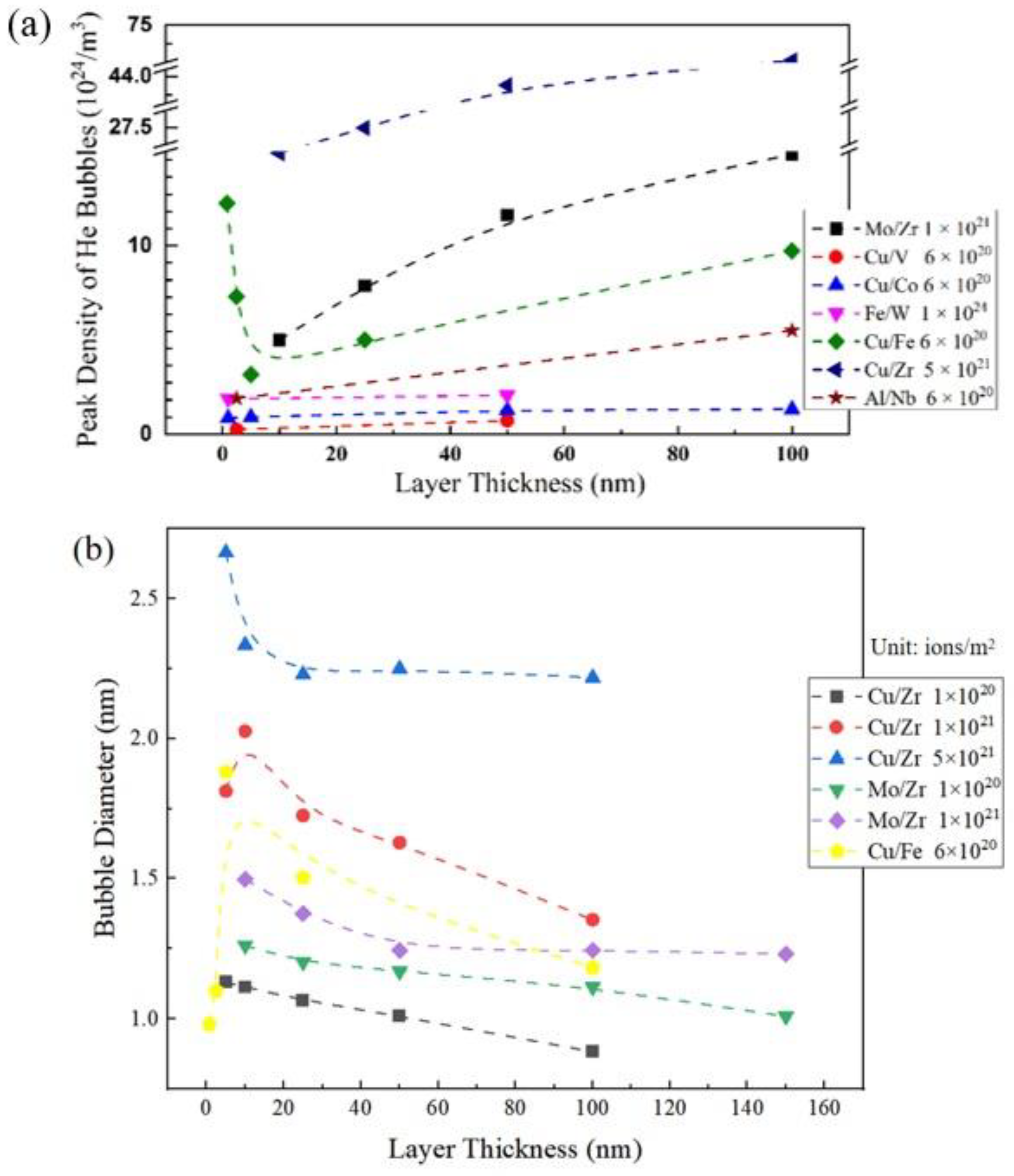
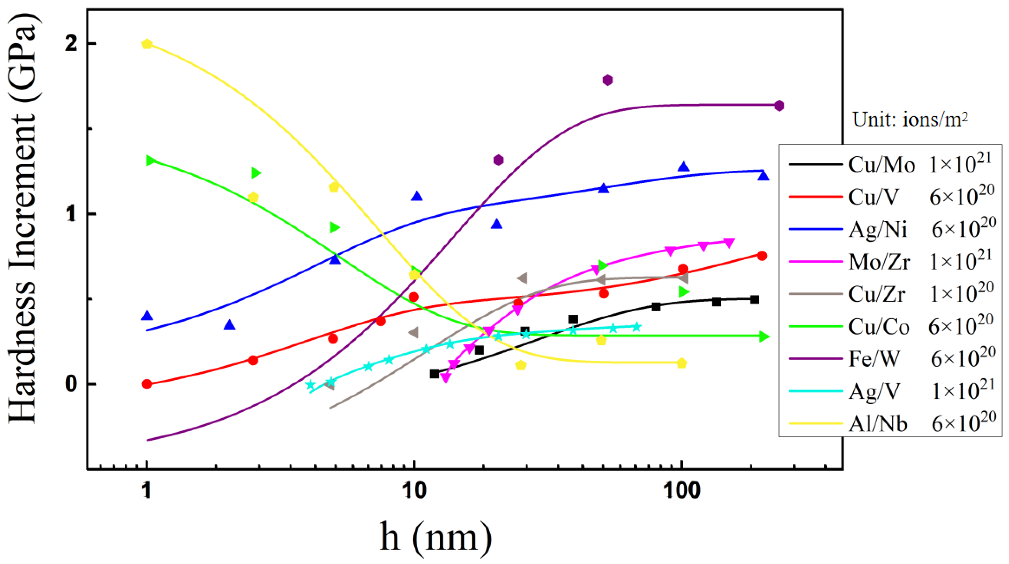
4. The Effect of Layer Thickness on the Irradiation Behaviors of Multilayer Films

Upon irradiation by energetic particles, materials often experience severe damage in the form of a drastic increase in defect density as well as significant degradation of their mechanical and physical properties [31,96]. A large number of experimental and simulation studies have reported that multilayer structures exhibit enhanced irradiation resistance due to the high density of interfaces [82,83,84,85,86,97,98,99,100,101]. The density and type of the interface, i.e., coherency and miscibility, are the main factors that can influence the irradiation behaviors of multilayer films. As mentioned above, the coherency of the multilayer films is closely related to the layer thickness. The miscibility of multilayer films is independent of layer thickness but can be altered under irradiation [57,84,102], which makes it hard to control. The effects of coherency on the irradiation behaviors of multilayer films have been widely studied [58,81,82]. This review focuses on the relationship between the layer thickness of multilayer films and their irradiation behaviors. A summary of previous studies on various metallic multilayer films irradiated by different sources is listed in Table 5.
The thickness of individual layers can be easily manipulated by magnetron sputtering, as mentioned above. This advantage has made magnetron sputtering a popular method to prepare multilayer films and investigate their irradiation behaviors. When the total thickness of the multilayer films is constant, the thinner the layer thickness, the higher the interface density, which may significantly affect the irradiation behavior. However, some mechanical properties, such as the hardness, wear resistance, and crystallinity of multilayer films, could deteriorate if the individual layer thickness decreases to a certain level [79,84]. Further investigations will undoubtedly be beneficial for translating this concept into a practical option for irradiation-resistant materials.
Under high-energy ion bombardment, the formation, accumulation, and evolution of a large number of defects will cause deterioration of the crystallinity and eventually cause the failure of materials [117]. Amorphization can be induced when the defect density is high enough. In general, the degeneration of crystallinity can be observed in XRD patterns in which diffraction peaks are broadened and intensities are reduced, as shown in Figure 10. The reduction in intensity indicates lattice disorder due to irradiation-induced defects and peak broadening is usually related to the microstrain caused by the absorption of interstitials during irradiation [4]. As mentioned above, reducing the layer thickness can effectively decrease the density of irradiation-induced defects, which is responsible for the suppression of amorphization. This phenomenon exists in many multilayer films, such as Cu/Fe [56], Cu/Co [76], Cu/Zr [84], and Mo/Zr [92]. Figure 10a shows the XRD patterns of Cu/Co multilayer films with different layer thicknesses before and after irradiation [76]. Irradiation exerts less influence on the crystallinity when the layer thickness becomes smaller, which manifests as the mitigated reduction in Cu (200) and Co (200) peaks after irradiation. When the layer thickness is below 10 nm, the coherent interface becomes dominant and the superlattice structure appears. Irradiation leads to diminished peak intensity with an insignificant peak shift. Figure 10b shows calculated results that demonstrate the evolution of the integrated intensity diffraction in the region of 38°–45° for Cu/W multilayer films with different layer thicknesses after different doses of He irradiation. The diffraction peaks in this area mainly refer to W (110) and Cu (111), as shown in Figure 8a. When the layer thickness is 5–50 nm, the intensity ratio decreases with increasing irradiation doses and eventually reaches a plateau, whereas the ratio continues to decrease when the layer thickness is 2.5 nm due to the deterioration of the crystallinity. The anomalous data at 5 nm may be attributed to a restoration process of the crystallite texture after irradiation with 6 × 10²¹ ions/m2 [4].
Irradiation-induced swelling and embrittlement, especially for metallic materials, also cause disastrous irradiation damage in a nuclear reactor environment [118,119]. Generally, these issues are introduced by nuclear transmutation during neutron irradiation, which will introduce a high density of gas atoms to materials, such as hydrogen (H) and helium (He). Consequently, the service life of materials is significantly diminished [120,121,122].
Due to the extremely low solubility of gas atoms in metals, they are prone to accumulate and form bubbles [58]. Experimental evidence has shown that the solubility of He atoms inside the metal is much lower than that at the interfaces [123]. Therefore, high-density interfaces can effectively absorb He atoms. In addition, high-density interfaces can suppress the formation of vacancy clusters, which are prone to combining with He atoms, causing swelling and embrittlement. Therefore, by decreasing the layer thickness (i.e., increasing the density of interfaces), the damage caused by He bubbles and vacancies can be effectively alleviated.
Figure 11a presents the density of He bubbles in the peak damage areas of various multilayer films, including five multilayer films, under different fluences of He ion irradiation. There is a clear trend of the peak density of He bubbles decreasing with decreasing layer thickness due to the increased interface density.
Notably, there are special cases when the film thickness is too small. For Cu/Fe multilayer films under 6 × 10²⁰ ions/m2 He irradiation with a layer thickness f less than 5 nm, the density of He bubbles increases with the decrease in layer thickness. This phenomenon is attributed to increased coherency [56]. The effects of coherent and incoherent interfaces on the irradiation resistance of multilayer films have been systematically described [58]. Generally, because the distortion and interfacial energy of coherent interfaces are smaller than their incoherent counterparts, the ability of coherent interfaces to absorb He and vacancies is lower, and therefore the density of irradiation-induced He bubbles increases with interface coherency [95]. Nonetheless, the diameter of He bubbles significantly decreases with the decrease in the layer thickness, as shown in Figure 11b, indicating that the rate of the overall swelling in Cu/Fe multilayer films still decreases with decreasing layer thickness, even below 5 nm [56].
In addition to Cu/Fe, several multilayer systems reveal a general trend in which the diameter of He bubbles decreases with decreasing layer thickness, as shown in Figure 11b. For the Cu/Zr multilayer films under He irradiation at 1 × 10²¹ ions/m2, the slight increase in the layer thickness of 10 nm may be caused by the dislocation punching effect, which increases the He concentration in the initial He bubbles. When the dislocation loop punches out from overpressured bubbles, the He bubble grows rapidly [84].
The irradiation-induced swelling can be reduced by suppressing the formation of gas bubbles and vacancy clusters. Therefore, it is easy to explain the tendency of the swelling rate to decrease with decreasing layer thickness. The relationships between the layer thickness and swelling rate of the Cu/V [5], Cu/Fe [56], and Cr/W [114] systems are summarized in Figure 12. In a study of Cr/W multilayer films, the swelling rate was measured by protecting part of the films through masks to avoid damage and leave the remaining portion exposed to irradiation. Then, the difference in thickness between the covered and uncovered portions was measured by atomic force microscopy (AFM) to calculate the rate of swelling. Although the swelling rates of the 50 and 5 nm Cr/W multilayer films were 7.35% and 6.55%, respectively, which is only a small difference of ~0.08%, the swelling rate of pure W was almost 20%, which is as high as three times that of the two mentioned above [114]. E. Fu et al. used a similar method to measure the swelling rate of Cu/V multilayer films with different layer thicknesses. The results showed a similar tendency. In addition, it was reported that the swelling rate of multilayer films with layer thicknesses of 2.5–50 nm was less than the rule-of-mixture (ROM) swelling in irradiated single-layer Cu and V films [5]. This result also applies to Ag/Ni multilayer films [110]. Y. Chen et al. calculated the swelling rate of the Cu/Fe multilayer films mainly based on the density and diameter of He bubbles (obtained from electron microscopy studies) and observed the same trend of a decreasing irradiation-induced swelling rate with decreasing layer thickness [56].
In addition to swelling, irradiation-induced hardening is also attributed to the accumulation of irradiation-induced defect clusters and gas bubbles [96]. For multilayer films, the mechanisms of irradiation hardening are distinguished at different layer thicknesses [97]. When the layer thickness of the multilayer films is 5–150 nm, the mechanism of hardening caused by decreasing layer thickness corresponds to the confined layer slip (CLS) model [84,92,124]. Under this circumstance, the gas bubbles in the layers act as barriers to sliding dislocations, leading to irradiation-induced hardening [61,125,126]. When the layer thickness of the multilayer films is below 5 nm, the dislocations can cut through the layer interfaces and the mechanism of hardening caused by decreasing layer thickness corresponds to the interfacial barrier strength (IBS) model. In this case, the hardening effect is the result of both the lattice distortion and the obstacles inhibiting dislocations from crossing the interfaces with distributed gas bubbles [127,128].
For most multilayer films, such as Cu/Mo [129], Cu/V [5], Cu/Zr [84], Ag/Ni [110], Ag/V [130], Mo/Zr [92], and Fe/W [3], the hardening effect can be alleviated by decreasing the layer thickness, as shown in Figure 13. This tendency corresponds to the relationship between the layer thickness and the density of both irradiation-induced gas bubbles and defects. However, a few multilayer films, such as Al/Nb [57] and Cu/Co [76], show the opposite tendency. For the Al/Nb system, the transition of interface miscibility due to the formation of intermetallic compounds after irradiation could change the hardening behavior. In general, the volume of the intermetallic compounds produced by irradiation increases with the decrease in layer thickness. Therefore, the influence of intermetallic compounds on the hardness increment will be stronger with a smaller layer thickness. Considering that the intermetallic compound Nb3Al produced by irradiation is much harder than individual Al and Nb layers, the smaller the layer thickness, the more severe the irradiation hardening caused by the increased proportion of the Nb3Al intermediate phase [57].
For immiscible Cu/Co multilayer films, when the layer thickness is below 50 nm, the opposite tendency is caused by the different strengthening mechanisms before and after irradiation. The deformation mechanism before irradiation is dominated by the transmission of partial dislocations between the layers. After irradiation, a large number of gas bubbles at the interfaces prevent the movement of partial dislocations. Only full dislocations can transmit between layers, which is much more difficult and dramatically increases the hardness. Therefore, as the layer thickness decreases, the density of the interface increases, leading to an amplified hardening effect caused by irradiation [76]. When the layer thickness is above 50 nm, the density of stacking faults rises rapidly with increasing layer thickness; as a result, the effect of irradiation hardening becomes insignificant with greater layer thicknesses [76].
One should note that, besides the effects of layer thickness, the deposition temperature, rate, bias, target–substrate distance, and many other preparation parameters can also have a substantial influence on the irradiation behaviors of multilayer films by changing the microstructure. However, there are still many uncertainties and more systematic studies are needed to clarify the influences of the deposition parameters stated above.

5. Conclusions

In this review, the effects of deposition parameters on the microstructure evolution of multilayer films were discussed. In general, increasing the substrate temperature and bias voltage or reducing the distance between the target and substrate can enhance the energy of adatoms as well as the crystallinity of multilayer films. With rising deposition temperature, the crystal grains become larger and the interfaces tend to first flatten and then become rougher. New compounds may form between adjacent layers as the deposition temperature increases, which varies among different materials. With the increase in the bias, the texture and crystallinity may change, manifesting as the intensified crystallographic texture with close-packed planes. Additionally, with increased bias, columnar grains will be transformed to equiaxed grains. Nevertheless, the influential mechanisms of some parameters on the microstructure, such as the deposition rate, still need further investigation.
Furthermore, the effects of layer thickness on the microstructure were briefly discussed. For as-deposited multilayer films, when layer thickness increases, the interlayer stress increases, which modifies the surface morphology and increases the defect density. It also affects the crystal orientation and texture of the films. When multilayer films contain both columnar-growth and layered-growth layers, the flatness and continuity of the films will be reduced if the layered-growth layers are not thick enough to cover the columnar-growth layers. Furthermore, the interface coherency may also change with different layer thicknesses. In many cases, a small layer thickness can promote interface coherency.
The layer thickness also greatly influences the irradiation behaviors of multilayer films. Irradiation-induced defects, gas bubbles, etc., are suppressed due to the high density of interfaces, thereby alleviating irradiation-induced hardening, swelling, embrittlement, and amorphization. In general, multilayer films with smaller layer thicknesses exhibit better irradiation stability. However, special cases exist. For instance, irradiation can increase the hardness more significantly for some multilayer films with smaller layer thicknesses. Thus, although multilayer films have been extensively studied, further investigations are required to explore their many possible applications.

Author Contributions

J.N.: Have made substantial contributions to the conception of the work; And drafting the work; And agreement to be accountable for all aspects of the work in ensuring that questions related to the accuracy or integrity of any part of the work are appropriately investigated and resolved. J.L.: Have made substantial contributions to the conception of the work; And revising it critically; And final approval of the version to be published; And agreement to be accountable for all aspects of the work in ensuring that questions related to the accuracy or integrity of any part of the work are appropriately investigated and resolved. J.J.: Have made substantial contributions to the interpretation of data for the work; And revising it critically; And final approval of the version to be published; And agreement to be accountable for all aspects of the work in ensuring that questions related to the accuracy or integrity of any part of the work are appropriately investigated and resolved. J.H.: Have made substantial contributions to the interpretation of data for the work; And revising it critically; And final approval of the version to be published; And agreement to be accountable for all aspects of the work in ensuring that questions related to the accuracy or integrity of any part of the work are appropriately investigated and resolved. H.C.: Have made substantial contributions to the interpretation of data for the work; And revising it critically; And final approval of the version to be published; And agreement to be accountable for all aspects of the work in ensuring that questions related to the accuracy or integrity of any part of the work are appropriately investigated and resolved. X.L. (Xuesong Leng): Have made substantial contributions to the interpretation of data for the work; AND revising it critically; And final approval of the version to be published; And agreement to be accountable for all aspects of the work in ensuring that questions related to the accuracy or integrity of any part of the work are appropriately investigated and resolved. X.L. (Xiangli Liu): Have made substantial contributions to the conception of the work; And drafting the work; And agreement to be accountable for all aspects of the work in ensuring that questions related to the accuracy or integrity of any part of the work are appropriately investigated and resolved. All authors have read and agreed to the published version of the manuscript.

Funding

This research study was funded by the financial support of the National Natural Science Foundation of China (number 12005048), the Natural Science Foundation of Shenzhen (the Stable Support Plan Program, number GXWD20201230155427003-20200822141815001), the Guangdong Basic and Applied Basic Research Foundation (number 2021A1515012411), and the Support Plan for Core Technology Research and Engineering Verification of Development and Reform Commission of Shenzhen Municipality (number 202100036).

Institutional Review Board Statement

Not applicable.

Informed Consent Statement

Not applicable.

Data Availability Statement

The data presented in this study are available upon request from the corresponding author.

Conflicts of Interest

The authors declare no conflict of interest.

References

  1. Chen, W.; Lin, Y.; Zheng, J.; Zhang, S.; Liu, S.; Kwon, S. Preparation and characterization of CrAlN/TiAlSiN nano-multilayers by cathodic vacuum arc. Surf. Coat. Technol. 2015, 265, 205–211. [Google Scholar] [CrossRef]
  2. Budiman, A.; Li, N.; Wei, Q.; Baldwin, J.; Xiong, J.; Luo, H.; Trugman, D.; Jia, Q.; Tamura, N.; Kunz, M.; et al. Growth and structural characterization of epitaxial Cu/Nb multilayers. Thin Solid Films 2010, 519, 4137–4143. [Google Scholar] [CrossRef]
  3. Li, N.; Fu, E.; Wang, H.; Carter, J.; Shao, L.; Maloy, S.; Misra, A.; Zhang, X. He ion irradiation damage in Fe/W nanolayer films. J. Nucl. Mater. 2009, 389, 233–238. [Google Scholar] [CrossRef]
  4. Gao, Y.; Yang, T.; Xue, J.; Yan, S.; Zhou, S.; Wang, Y.; Kwok, D.T.; Chu, P.; Zhang, Y. Radiation tolerance of Cu/W multilayered nanocomposites. J. Nucl. Mater. 2011, 413, 11–15. [Google Scholar] [CrossRef]
  5. Fu, E.; Misra, A.; Wang, H.; Shao, L.; Zhang, X. Interface enabled defects reduction in helium ion irradiated Cu/V nanolayers. J. Nucl. Mater. 2010, 407, 178–188. [Google Scholar] [CrossRef]
  6. Ham, B.; Junkaew, A.; Arroyave, R.; Chen, J.; Wang, H.; Wang, P.; Majewski, J.; Park, J.; Zhou, H.C.; Arvapally, R.K.; et al. Hydrogen sorption in orthorhombic Mg hydride at ultra-low temperature. Int. J. Hydrogen Energy 2013, 38, 8328–8341. [Google Scholar] [CrossRef]
  7. Chen, P.; Zhu, M. Recent progress in hydrogen storage. Mater. Today 2008, 11, 36–43. [Google Scholar] [CrossRef]
  8. Piramanayagam, S. Perpendicular recording media for hard disk drives. J. Appl. Phys. 2007, 102, 011301. [Google Scholar] [CrossRef]
  9. Moser, A.; Takano, K.; Margulies, D.T.; Albrecht, M.; Sonobe, Y.; Ikeda, Y.; Sun, S.; Fullerton, E.E. Magnetic recording: Advancing into the future. J. Phys. D Appl. Phys. 2002, 35, R157–R167. Available online: https://iopscience.iop.org/article/10.1088/0022-3727/35/19/201/meta (accessed on 25 October 2021). [CrossRef]
  10. Hu, H.; Gao, W.; Zang, R.; Gao, J.; Tang, S.; Li, X.; Liang, L.; Zhang, H.; Cao, H.J.A.F.M. Direct growth of vertically orientated nanocavity arrays for plasmonic color generation. Adv. Funct. Mater. 2020, 30, 2002287. [Google Scholar] [CrossRef]
  11. Varghese, B.; Piramanayagam, S.; Yang, Y.; Wong, S.K.; Tan, H.K.; Lee, W.K.; Okamoto, I. Equiatomic CoPt thin films with extremely high coercivity. J. Appl. Phys. 2014, 115, 17. [Google Scholar] [CrossRef]
  12. Liang, J.; Liu, Q.; Li, T.; Luo, Y.; Lu, S.; Shi, X.; Zhang, F.; Asiri, A.M.; Sun, X. Magnetron sputtering enabled sustainable synthesis of nanomaterials for energy electrocatalysis. Green Chem. 2021, 23, 2834–2867. Available online: https://pubs.rsc.org/en/content/articlehtml/2021/gc/d0gc03994b (accessed on 25 October 2021). [CrossRef]
  13. Park, K.-I.; Xu, S.; Liu, Y.; Hwang, G.-T.; Kang, S.-J.L.; Wang, Z.L.; Lee, K.J. Piezoelectric BaTiO3 thin film nanogenerator on plastic substrates. Nano Lett. 2010, 10, 4939–4943. Available online: https://pubs.acs.org/doi/abs/10.1021/nl102959k (accessed on 25 October 2021). [CrossRef] [PubMed] [Green Version]
  14. Webb, J.B.; Lockwood, D.; Gnezdilov, V. Magnetron sputter epitaxy and characterization of InSb/In1−xAlxSb strained layer superlattices. J. Cryst. Growth 1994, 137, 405–414. [Google Scholar] [CrossRef]
  15. Wang, M.; Fan, Z. Optics coatings by magnetron sputtering deposition. In Proceedings of the Third International Conference on Thin Film Physics and Applications, Shanghai, China, 20 February 1998; pp. 130–132. Available online: https://www.spiedigitallibrary.org/conference-proceedings-of-spie/3175/0000/Optics-coatings-by-magnetron-sputtering-deposition/10.1117/12.300652.short (accessed on 25 October 2021).
  16. Ellmer, K. Magnetron sputtering of transparent conductive zinc oxide: Relation between the sputtering parameters and the electronic properties. J. Phys. D Appl. Phys. 2000, 33, R17–R32. [Google Scholar] [CrossRef]
  17. Tang, W.; Xu, K.W.; Wang, P.; Li, X. Characterization of the surface roughness and nanoindentation hardness of Au/NiCr/Ta multilayers. Acta Metall. Sinica. 2002, 38, 449–452. Available online: http://www.jmonline.org/article/doi/10.3321/j.issn:0412-1961.2002.05.001 (accessed on 25 October 2021).
  18. Lenis, J.; Gómez, M.; Bolívar, F.J.S.; Technology, C. Effect of deposition temperature and target-substrate distance on the structure, phases, mechanical and tribological properties of multi-layer HA-Ag coatings obtained by RF magnetron sputtering. Surf. Coat. Technol. 2019, 378, 124936. [Google Scholar] [CrossRef]
  19. Yang, J.; Wang, C.; Ouyang, K.; Tao, D.-P.; Yang, Y. Effects of Deposition Temperature and Growth Interruption on Ge/Si Multilayer Films Prepared by Ion Beam Sputtering. J. Synth. Cryst. 2010, 39, 945–950. [Google Scholar] [CrossRef]
  20. Safran, G.; Reinhard, C.; Ehiasarian, A.; Barna, P.B.; Szekely, L.; Geszti, O.; Hovsepian, P.E. Influence of the bias voltage on the structure and mechanical performance of nanoscale multilayer CrAlYN/CrN physical vapor deposition coatings. J. Vac. Sci. Technol. A 2009, 27, 174–182. [Google Scholar] [CrossRef]
  21. Monclús, M.A.; Karlik, M.; Callisti, M.; Frutos, E.; Llorca, J.; Polcar, T.; Molina-Aldareguía, J.M. Microstructure and mechanical properties of physical vapor deposited Cu/W nanoscale multilayers: Influence of layer thickness and temperature. Thin Solid Film. 2014, 571, 275–282. [Google Scholar] [CrossRef] [Green Version]
  22. Zheng, X.-H.; Liu, T.; Wang, G.-Q.; Yang, S.-Y.; Wang, Z.-S.; Yang, F.-E. Microstructure and tribological behaviors of magnetron sputtered WS2/Fe/aC/Fe multilayer films with various deposition temperatures. Vacuum 2020, 179, 109550. [Google Scholar] [CrossRef]
  23. Domínguez-Crespo, M.; Torres-Huerta, A.; Rodríguez, E.; González-Hernández, A.; Brachetti-Sibaja, S.; Dorantes-Rosales, H.; López-Oyama, A. Effect of deposition parameters on structural, mechanical and electrochemical properties in Ti/TiN thin films on AISI 316L substrates produced by r. f. magnetron sputtering. J. Alloys Compd. 2018, 746, 688–698. [Google Scholar] [CrossRef]
  24. Zhangyu, Z.; Han, X.; Song, W.; Qingzhu, Z.; Daigiang, W.; Yuqing, C.; Xinghua, F. Fabrication and superconducting property of MgB2/Mo multilayer films. Rare Met. Mater. Eng. 2019, 48, 2711–2715. Available online: https://kns.cnki.net/kcms/detail/detail.aspx?dbcode=CJFD&dbname=CJFDLAST2019&filename=COSE201908048&uniplatform=NZKPT&v=LXX2Z_7qkhlLYaXOlR70-NnWUME8B3wOSkD8APhZpBUc94GmFNZQ_ofnaXiuHpTl (accessed on 25 October 2021).
  25. Pogrebnjak, A.; Smyrnova, K.; Bondar, O. Nanocomposite multilayer binary nitride coatings based on transition and refractory metals: Structure and properties. Coatings 2019, 9, 155. [Google Scholar] [CrossRef] [Green Version]
  26. Hu, M.; Liu, Y.; Lai, Z.Q. Technological parameters and electrical properties of Ti/TiN multilayer films prepared by magnetron sputtering. Mater. Sci. Forum 2010, 654–656, 1752–1755. [Google Scholar] [CrossRef]
  27. Yang, K.M.; Tang, P.Z.; Zhang, Q.; Ma, H.Y.; Liu, E.Q.; Li, M.; Zhang, X.; Li, J.; Liu, Y.; Fan, T.X. Enhanced defect annihilation capability of the graphene/copper interface: An in situ study. Scr. Mater. 2021, 203, 114001. [Google Scholar] [CrossRef]
  28. Zinkle, S.; Singh, B. Analysis of displacement damage and defect production under cascade damage conditions. J. Nucl. Mater. 1993, 199, 173–191. [Google Scholar] [CrossRef]
  29. Phythian, W.; Stoller, R.; Foreman, A.; Calder, A.; Bacon, D. A comparison of displacement cascades in copper and iron by molecular dynamics and its application to microstructural evolution. J. Nucl. Mater. 1995, 223, 245–261. [Google Scholar] [CrossRef]
  30. Jenkins, M.; Kirk, M.; Phythian, W. Experimental studies of cascade phenomena in metals. J. Nucl. Mater. 1993, 205, 16–30. [Google Scholar] [CrossRef] [Green Version]
  31. Was, G.S. Fundamentals of Radiation Materials Science: Metals and Alloys; Springer: Berlin/Heidelberg, Germany, 2016; Available online: https://sc.panda321.com/extdomains/books.google.com/books?hl=zh-CN&lr=&id=yDGmDAAAQBAJ&oi=fnd&pg=PR8&dq=Fundamentals+of+Radiation+Materials+Science:+Metals+and+Alloys&ots=FlfGekj1Sy&sig=LKY1-nVdYw6jOAD6weAWb16Ol8Q (accessed on 25 October 2021).
  32. Ullmaier, H. The influence of helium on the bulk properties of fusion reactor structural materials. Nucl. Fusion 1984, 24, 1039–1083. [Google Scholar] [CrossRef]
  33. Zinkle, S.J.; Ghetta, V. Microstructures and Mechanical Properties of Irradiated Metals and Alloys, Materials Issues for Generation IV Systems, Dordrecht, 2008; Ghetta, V., Gorse, D., Mazière, D., Pontikis, V., Eds.; Springer: Berlin/Heidelberg, Germany, 2008; pp. 227–244. [Google Scholar]
  34. Odette, G.; Alinger, M.; Wirth, B. Recent Developments in Irradiation-Resistant Steels. Annu. Rev. Mater. Res. 2008, 38, 471–503. [Google Scholar] [CrossRef]
  35. Du, C.; Jin, S.; Fang, Y.; Li, J.; Hu, S.; Yang, T.; Zhang, Y.; Huang, J.; Sha, G.; Wang, Y.; et al. Ultrastrong nanocrystalline steel with exceptional thermal stability and radiation tolerance. Nat. Commun. 2018, 9, 5389. [Google Scholar] [CrossRef]
  36. Shang, Z.; Ding, J.; Fan, C.; Chen, D.; Li, J.; Zhang, Y.; Wang, Y.; Wang, H.; Zhang, X. He ion irradiation response of a gradient T91 steel. Acta Mater. 2020, 196, 175–190. [Google Scholar] [CrossRef]
  37. Shang, Z.; Fan, C.; Ding, J.; Xue, S.; Gabriel, A.; Shao, L.; Voisin, T.; Wang, Y.M.; Niu, T.; Li, J.; et al. Heavy ion irradiation response of an additively manufactured 316LN stainless steel. J. Nucl. Mater. 2021, 546, 152745. [Google Scholar] [CrossRef]
  38. Shang, Z.; Fan, C.; Xue, S.; Ding, J.; Li, J.; Voisin, T.; Wang, Y.M.; Wang, H.; Zhang, X. Response of solidification cellular structures in additively manufactured 316 stainless steel to heavy ion irradiation: An in situ study. Mater. Res. Lett. 2019, 7, 290–297. [Google Scholar] [CrossRef] [Green Version]
  39. Chen, Y.; Li, J.; Yu, K.; Wang, H.; Kirk, M.; Li, M.; Zhang, X. In situ studies on radiation tolerance of nanotwinned Cu. Acta Mater. 2016, 111, 148–156. [Google Scholar] [CrossRef] [Green Version]
  40. Li, J.; Chen, Y.; Wang, H.; Zhang, X. In situ studies on twin-thickness-dependent distribution of defect clusters in heavy ion-irradiated nanotwinned Ag. Met. Mater. Trans. A 2017, 48, 1466–1473. [Google Scholar] [CrossRef]
  41. Li, J.; Xie, D.; Xue, S.; Fan, C.; Chen, Y.; Wang, H.; Wang, J.; Zhang, X. Superior twin stability and radiation resistance of nanotwinned Ag solid solution alloy. Acta Mater. 2018, 151, 395–405. [Google Scholar] [CrossRef]
  42. Fan, C.; Xie, D.; Li, J.; Shang, Z.; Chen, Y.; Xue, S.; Wang, J.; Li, M.; El-Azab, A.; Wang, H.; et al. 9R phase enabled superior radiation stability of nanotwinned Cu alloys via in situ radiation at elevated temperature. Acta Mater. 2019, 167, 248–256. [Google Scholar] [CrossRef] [Green Version]
  43. Li, J.; Yu, K.Y.; Chen, Y.; Song, M.; Wang, H.; Kirk, M.A.; Li, M.; Zhang, X. In situ study of defect migration kinetics and self-healing of twin boundaries in heavy ion irradiated nanotwinned metals. Nano Lett. 2015, 15, 2922–2927. [Google Scholar] [CrossRef] [PubMed]
  44. Niu, T.; Li, J.; Zhang, Y.; Cho, J.; Ding, J.; Su, R.; Xue, S.; Fan, C.; Shang, Z.; Chen, D.; et al. In-situ studies on the mechanical properties of He ion irradiated nanotwinned Ag. J. Nucl. Mater. 2020, 540, 152392. [Google Scholar] [CrossRef]
  45. Yu, K.Y.; Fan, C.; Chen, Y.; Li, J.; Zhang, X. Recent Studies on the Microstructural Response of Nanotwinned Metals to In Situ Heavy Ion Irradiation. JOM 2020, 72, 160–169. [Google Scholar] [CrossRef]
  46. Fan, C.; Sreekar, A.; Shang, Z.; Li, J.; Li, M.; Wang, H.; El-Azab, A.; Zhang, X. Radiation induced nanovoid shrinkage in Cu at room temperature: An in situ study. Scr. Mater. 2019, 166, 112–116. [Google Scholar] [CrossRef]
  47. Fan, Z.; Li, Q.; Li, J.; Xue, S.; Wang, H.; Zhang, X. Tailoring plasticity of metallic glasses via interfaces in Cu/amorphous CuNb laminates. J. Mater. Res. 2017, 32, 2680–2689. [Google Scholar] [CrossRef]
  48. Li, J.; Chen, Y.; Wang, H.; Zhang, X. In situ study on enhanced heavy ion irradiation tolerance of porous Mg. Scr. Mater. 2018, 144, 13–17. [Google Scholar] [CrossRef]
  49. Li, J.; Fan, C.; Ding, J.; Xue, S.; Chen, Y.; Li, Q.; Wang, H.; Zhang, X. In situ heavy ion irradiation studies of nanopore shrinkage and enhanced radiation tolerance of nanoporous Au. Sci. Rep. 2017, 7, 39484. [Google Scholar] [CrossRef] [PubMed]
  50. Li, J.; Fan, C.; Li, Q.; Wang, H.; Zhang, X. In situ studies on irradiation resistance of nanoporous Au through temperature-jump tests. Acta Mater. 2018, 143, 30–42. [Google Scholar] [CrossRef]
  51. Li, J.; Wang, H.; Zhang, X. A review on the radiation response of nanoporous metallic materials. JOM 2018, 70, 2753–2764. [Google Scholar] [CrossRef]
  52. Niu, T.; Nasim, M.; Annadanam, R.G.S.; Fan, C.; Li, J.; Shang, Z.; Xue, Y.; El-Azab, A.; Wang, H.; Zhang, X. Recent studies on void shrinkage in metallic materials subjected to in situ heavy ion irradiations. JOM 2020, 72, 4008–4016. [Google Scholar] [CrossRef]
  53. Ackland, G. Controlling Radiation Damage. Science 2010, 327, 1587–1588. [Google Scholar] [CrossRef]
  54. Callisti, M.; Karlik, M.; Polcar, T. Bubbles formation in helium ion irradiated Cu/W multilayer nanocomposites: Effects on structure and mechanical properties. J. Nucl. Mater. 2016, 473, 18–27. [Google Scholar] [CrossRef] [Green Version]
  55. Wang, M.; Beyerlein, I.J.; Zhang, J.; Han, W.-Z. Defect-interface interactions in irradiated Cu/Ag nanocomposites. Acta Mater. 2018, 160, 211–223. [Google Scholar] [CrossRef]
  56. Chen, Y.; Fu, E.; Yu, K.; Song, M.; Liu, Y.; Wang, Y.; Wang, H.; Zhang, X. Enhanced radiation tolerance in immiscible Cu/Fe multilayers with coherent and incoherent layer interfaces. J. Mater. Res. 2015, 30, 1300–1309. Available online: https://www.cambridge.org/core/journals/journal-of-materials-research/article/enhanced-radiation-tolerance-in-immiscible-cufe-multilayers-with-coherent-and-incoherent-layer-interfaces/CC962813E8E65989C338C1A70039B38F (accessed on 25 October 2021). [CrossRef]
  57. Li, N.; Martin, M.; Anderoglu, O.; Misra, A.; Shao, L.; Wang, H.; Zhang, X. He ion irradiation damage in Al/Nb multilayers. J. Appl. Phys. 2009, 105, 123522. [Google Scholar] [CrossRef]
  58. Zhang, X.; Hattar, K.; Chen, Y.; Shao, L.; Li, J.; Sun, C.; Yu, K.; Li, N.; Taheri, M.L.; Wang, H.; et al. Radiation damage in nanostructured materials. Prog. Mater. Sci. 2018, 96, 217–321. [Google Scholar] [CrossRef]
  59. Chen, Y.; Li, N.; Bufford, D.C.; Li, J.; Hattar, K.; Wang, H.; Zhang, X. In situ study of heavy ion irradiation response of immiscible Cu/Fe multilayers. J. Nucl. Mater. 2016, 475, 274–279. [Google Scholar] [CrossRef] [Green Version]
  60. Niu, T.; Zhang, Y.; Cho, J.; Li, J.; Wang, H.; Zhang, X. Thermal stability of immiscible Cu-Ag/Fe triphase multilayers with triple junctions. Acta Mater. 2021, 208, 116679. [Google Scholar] [CrossRef]
  61. Misra, A.; Hirth, J.P.; Kung, H. Single-dislocation-based strengthening mechanisms in nanoscale metallic multilayers. Philos. Mag. A 2002, 82, 2935–2951. [Google Scholar] [CrossRef]
  62. Clemens, B.; Kung, H.; Barnett, S. Structure and strength of multilayers. MRS Bull. 1999, 24, 20–26. [Google Scholar] [CrossRef]
  63. Zhang, Z.; Lagally Max, G. Atomistic processes in the early stages of thin-film growth. Science 1997, 276, 377–383. Available online: https://www.science.org/doi/full/10.1126/science.276.5311.377 (accessed on 25 October 2021). [CrossRef]
  64. Yamada, M.; Hotta, Y.; Yanagawa, T.; Ohtake, M.; Kirino, F.; Futamoto, M. Effect of substrate temperature on the ordered phase formation in Sm–Ni thin film deposited on Cu(111) underlayer. IEEE Trans. Magn. 2013, 50, 1–4. [Google Scholar] [CrossRef]
  65. Suzaki, Y.; Kawaguchi, A.; Murase, T.; Yuji, T.; Shikama, T.; Shin, D.-B.; Kim, Y.-K. Effect of substrate temperature on ZnO thin film fabrication by using an atmospheric pressure cold plasma generator. Phys. Status Solidi 2011, 8, 503–505. [Google Scholar] [CrossRef]
  66. Levi, A.C.; Kotrla, M. Theory and simulation of crystal growth. J. Phys. Condens. Matter 1997, 9, 299–344. [Google Scholar] [CrossRef]
  67. Sun, C.; Maloy, S.A.; Baldwin, K.; Wang, Y.; Valdez, J.A. Phase stability of Ni/Ni3Al multilayers under thermal annealing and irradiation. JOM 2020, 72, 3995–4001. Available online: https://link.springer.com/article/10.1007/s11837-020-04377-0 (accessed on 25 October 2021). [CrossRef]
  68. Pogrebnjak, A.D.; Ivashchenko, V.I.; Skrynskyy, P.L.; Bondar, O.V.; Konarski, P.; Załęski, K.; Jurga, S.; Coy, E. Experimental and theoretical studies of the physicochemical and mechanical properties of multi-layered TiN/SiC films: Temperature effects on the nanocomposite structure. Compos. Part B Eng. 2018, 142, 85–94. [Google Scholar] [CrossRef]
  69. Schürmann, U.; Takele, H.; Zaporojtchenko, V.; Faupel, F. Optical and electrical properties of polymer metal nanocomposites prepared by magnetron co-sputtering. Thin Solid Film. 2006, 515, 801–804. [Google Scholar] [CrossRef]
  70. Yanev, V.; Krischok, S.; Opitz, A.; Wurmus, H.; Schaefer, J.; Schwesinger, N.; Ahmed, S.-I.-U. Influence of the RF power on the deposition rate and the chemical surface composition of fluorocarbon films prepared in dry etching gas plasma. Surf. Sci. 2004, 566–568, 1229–1233. [Google Scholar] [CrossRef]
  71. Yamamoto, S.; Ichimura, H. Effect of substrate bias voltage on the properties of arc ion-plated TiN films onto high speed steels. J. Mater. Res. 1996, 11, 1149–1156. [Google Scholar] [CrossRef]
  72. Pogrebnjak, A.; Beresnev, V.; Bondar, O.; Postolnyi, B.; Załęski, K.; Coy, E.; Jurga, S.; Lisovenko, M.; Konarski, P.; Rebouta, L.; et al. Superhard CrN/MoN coatings with multilayer architecture. Mater. Des. 2018, 153, 47–59. [Google Scholar] [CrossRef]
  73. Mahieu, S.; Ghekiere, P.; Depla, D.; De Gryse, R. Biaxial alignment in sputter deposited thin films. Thin Solid Films 2006, 515, 1229–1249. [Google Scholar] [CrossRef] [Green Version]
  74. Zhang, H.; Ren, F.; Hong, M.; Xiao, X.; Cai, G.; Jiang, C. Structure and growth mechanism of V/Ag multilayers with differ-ent periodic thickness fabricated by magnetron sputtering deposition. J. Mater. Sci. Technol. 2014, 30, 1012–1019. [Google Scholar] [CrossRef]
  75. Fu, E.G.; Carter, J.; Swadener, G.; Misra, A.; Shao, L.; Wang, H.; Zhang, X. Size dependent enhancement of helium ion irradiation tolerance in sputtered Cu/V nanolaminates. J. Nucl. Mater. 2009, 385, 629–632. [Google Scholar] [CrossRef]
  76. Chen, Y.; Liu, Y.; Fu, E.; Sun, C.; Yu, K.; Song, M.; Li, J.; Wang, Y.; Wang, H.; Zhang, X. Unusual size-dependent strengthening mechanisms in helium ion-irradiated immiscible coherent Cu/Co nanolayers. Acta Mater. 2015, 84, 393–404. [Google Scholar] [CrossRef] [Green Version]
  77. Hou, Z.; Zhang, J.; Zhang, P.; Wu, K.; Li, J.; Wang, Y.; Liu, G.; Zhang, G.; Sun, J. Modulation-dependent deformation behavior and strengthening response in nanostructured Ti/Zr multilayers. Appl. Surf. Sci. 2020, 502, 144118. [Google Scholar] [CrossRef]
  78. Xu, J.; Kamiko, M.; Zhou, Y.; Yamamoto, R.; Li, G.; Gu, M. Superhardness effects of heterostructure NbN/TaN nanostructured multilayers. J. Appl. Phys. 2001, 89, 3674–3678. [Google Scholar] [CrossRef]
  79. Li, J.; Chen, Y.; Xue, S.; Wang, H.; Zhang, X. Comparison of size dependent strengthening mechanisms in Ag/Fe and Ag/Ni multilayers. Acta Mater. 2016, 114, 154–163. [Google Scholar] [CrossRef] [Green Version]
  80. Guo, Q.; Wan, L.; Yu, X.-X.; Vogel, F.; Thompson, G.B. Influence of phase stability on the in situ growth stresses in Cu/Nb multilayered films. Acta Mater. 2017, 132, 149–161. [Google Scholar] [CrossRef] [Green Version]
  81. Cao, Z.H.; Wei, M.Z.; Ma, Y.J.; Sun, C.; Lu, H.M.; Fan, Z.; Meng, X.K. Cyclic deformation induced strengthening and unusual rate sensitivity in Cu/Ru nanolayered films. Int. J. Plast. 2017, 99, 43–57. [Google Scholar] [CrossRef]
  82. Heinisch, H.; Gao, F.; Kurtz, R. The effects of interfaces on radiation damage production in layered metal composites. J. Nucl. Mater. 2004, 329–333, 924–928. [Google Scholar] [CrossRef]
  83. Zhou, Q.; Li, J.; Wang, F.; Huang, P.; Xu, K.; Lu, T. Strain rate sensitivity of Cu/Ta multilayered films: Comparison between grain boundary and heterophase interface. Scr. Mater. 2016, 111, 123–126. [Google Scholar] [CrossRef]
  84. Liang, X.Q.; Wang, Y.Q.; Zhao, J.T.; Wu, S.H.; Wu, K.; Liu, G.; Sun, J. Size- and ion-dose-dependent microstructural evolution and hardening in He-irradiated miscible Cu/Zr crystalline/crystalline nanolaminates. Surf. Coat. Technol. 2019, 366, 255–265. [Google Scholar] [CrossRef]
  85. Guo, Z.B.; Mi, W.B.; Li, J.Q.; Cheng, Y.; Zhang, X.X. Enhancement in anomalous Hall resistivity of Co/Pd multilayer and CoPd alloy by Ga + ion irradiation. EPL Europhys. Lett. 2014, 105, 46005. [Google Scholar] [CrossRef]
  86. Spasova, M.; Wiedwald, U.; Ramchal, R.; Farle, M.; Jergel, M.; Majkova, E.; Luby, S.; Senderak, R. Magnetization and Magnetic Anisotropy of Co/W Multilayers. Phys. Status Solidi 2001, 225, 449–457. [Google Scholar] [CrossRef]
  87. Hillebrands, B.; Dutcher, J.R. Origin of very large in-plane anisotropies in (110)-oriented Co/Pd and Co/Pt coherent super-lattices. Phys. Rev. B 1993, 47, 6126–6129. Available online: https://journals.aps.org/prb/abstract/10.1103/PhysRevB.47.6126 (accessed on 25 October 2021). [CrossRef]
  88. Majková, E.; Spasova, M.; Jergel, M.; Luby, S.; Okayasu, S.; Luches, A.; Martino, M.; Zubarev, E.; Brunel, M. Formation of granular-like structure of Ag/Co multilayers by excimer laser irradiation. Thin Solid Films 1999, 343–344, 214–217. [Google Scholar] [CrossRef]
  89. Yu, K.; Liu, Y.; Fu, E.; Wang, Y.; Myers, M.; Wang, H.; Shao, L.; Zhang, X. Comparisons of radiation damage in He ion and proton irradiated immiscible Ag/Ni nanolayers. J. Nucl. Mater. 2013, 440, 310–318. [Google Scholar] [CrossRef]
  90. Kim, C.; Qadri, S.B.; Yu, H.Y.; Kim, K.H.; Maruyama, B.; Edelstein, A.S. Synthesis and structure of ion-beam sputtered multilayer Fe/Ni films. J. Vac. Sci. Technol. A 1990, 8, 1407–1410. [Google Scholar] [CrossRef]
  91. Wu, Z.L.; Peng, T.X.; Cao, B.S.; Lei, M.K. X-ray diffraction and high resolution transmission electron microscopy charac-terization of intermetallics formed in Fe/Ti nanometer-scale multilayers during thermal annealing. Thin Solid Film. 2009, 517, 6553–6557. [Google Scholar] [CrossRef]
  92. Wu, S.; Cheng, P.; Wu, K.; Hou, Z.; Wang, Y.; Liang, X.; Li, J.; Kuang, J.; Zhang, J.; Liu, G.; et al. Effect of He-irradiation fluence on the size-dependent hardening and deformation of nanostructured Mo/Zr multilayers. Int. J. Plast. 2018, 111, 36–52. [Google Scholar] [CrossRef]
  93. Laptev, R.; Lomygin, A.; Krotkevich, D.; Syrtanov, M.; Kashkarov, E.; Bordulev, Y.; Siemek, K.; Kobets, A. Effect of Proton Irradiation on the Defect Evolution of Zr/Nb Nanoscale Multilayers. Metals 2020, 10, 535. [Google Scholar] [CrossRef] [Green Version]
  94. Hou, Z.Q.; Zhang, J.Y.; Li, J.; Wang, Y.Q.; Wu, K.; Liu, G.; Zhang, G.J.; Sun, J. Phase transformation-induced strength sof-tening in Ti/Ta nanostructured multilayers: Coherent interface vs. phase boundary. Mater. Sci. Eng. A 2017, 684, 78–83. [Google Scholar] [CrossRef]
  95. Zhang, Y.; Xue, S.; Li, Q.; Li, J.; Ding, J.; Niu, T.; Su, R.; Wang, H.; Zhang, X. Size dependent strengthening in high strength nanotwinned Al/Ti multilayers. Acta Mater. 2019, 175, 466–476. [Google Scholar] [CrossRef]
  96. Zinkle, S.J. Radiation-Induced Effects on Microstructure. Compr. Nucl. Mater. 2020, 1, 91–129. Available online: https://www.researchgate.net/publication/255249921 (accessed on 25 October 2021).
  97. He, X.; Liang, S.-H.; Li, J.-H.; Liu, B.-X. Atomistic mechanism of interfacial reaction and asymmetric growth kinetics in an immiscible Cu/Ru system at equilibrium. Phys. Rev. B 2007, 75, 045431. Available online: https://journals.aps.org/prb/abstract/10.1103/PhysRevB.75.045431 (accessed on 25 October 2021). [CrossRef]
  98. Demkowicz, M.J.; Hoagland, R.G.; Hirth, J.P. Interface structure and radiation damage resistance in Cu-Nb multilayer nanocomposites. Phys. Rev. Lett. 2008, 100, 136102. [Google Scholar] [CrossRef]
  99. Abdolrahim, N.; Zbib, H.M.; Bahr, D.F. Multiscale modeling and simulation of deformation in nanoscale metallic multi-layer systems. Int. J. Plast. 2014, 52, 33–50. [Google Scholar] [CrossRef]
  100. Misra, A.; Demkowicz, M.J.; Zhang, X.; Hoagland, R.G. The radiation damage tolerance of ultra-high strength nanolayered composites. JOM 2007, 59, 62–65. [Google Scholar] [CrossRef]
  101. Ziegler, J.F.; Biersack, J.P. The stopping and range of ions in matter. In Treatise on Heavyion Science; Springer: Berlin/Heidelberg, Germany, 1985; pp. 93–129. Available online: https://link.springer.com/chapter/10.1007/978-1-4615-8103-1_3 (accessed on 25 October 2021).
  102. Mao, S.; Shu, S.; Zhou, J.; Averback, R.S.; Dillon, S.J. Quantitative comparison of sink efficiency of Cu–Nb, Cu–V and Cu–Ni interfaces for point defects. Acta Mater. 2015, 82, 328–335. [Google Scholar] [CrossRef] [Green Version]
  103. Li, N.; Carter, J.; Misra, A.; Shao, L.; Wang, H.; Zhang, X. The influence of interfaces on the formation of bubbles in He-ion-irradiated Cu/Mo nanolayers. Philos. Mag. Lett. 2011, 91, 18–28. [Google Scholar] [CrossRef]
  104. Zhang, L.; Gao, R.; Hou, J.; Zhao, B.; Sun, M.; Hao, T.; Xie, Z.; Liu, R.; Wang, X.; Fang, Q.; et al. Study on thermal stability and irradiation response of copper/iron nano-multilayer composite fabricated by cross accumulative roll bonding. J. Nucl. Mater. 2021, 543, 152548. [Google Scholar] [CrossRef]
  105. Liang, X.; Zhang, J.; Wang, Y.; Wu, S.; Zeng, F.; Wu, K.; Liu, G.; Zhang, G.; Sun, J. Tuning the size-dependent He-irradiated tolerance and strengthening behavior of crystalline/amorphous Cu/Ta nanostructured multilayers. Mater. Sci. Eng. A 2016, 672, 153–160. [Google Scholar] [CrossRef]
  106. Suharyadi, E.; Natsume, S.; Kato, T.; Tsunashima, S.; Iwata, S. Modification of the microstructure and magnetic properties of Ga-Ion-Irradiated Co/Pd multilayer film for future planar media. Trans. Magn. Soc. Jpn. 2005, 5, 125–130. [Google Scholar] [CrossRef]
  107. Bagchi, S.; Anwar, S.; Lalla, N. Effect of swift heavy ion irradiation in W/Co multilayer structures. Nucl. Instrum. Methods Phys. Res. Sect. B Beam Interact. Mater. At. 2010, 268, 1601–1606. [Google Scholar] [CrossRef]
  108. Kavita, S.; Reddy, V.R.; Amirthapandian, S.; Gupta, A.; Panigrahi, B.K. Si+ ion irradiation in a Co/Pt multilayer system. J. Phys. Condens. Matter 2009, 21, 096003. [Google Scholar] [CrossRef] [PubMed]
  109. Amirthapandian, S.; Panigrahi, B.K.; Srivastava, A.K.; Gupta, A.; Nair, K.G.M.; Nandedkar, R.V.; Narayanasamy, A. Irra-diation induced metastable phase formation in thermally immiscible Co–Ag multilayers. Nucl. Instrum. Methods Phys. Res. Sect. B Beam Interact. Mater. At. 2003, 212, 140–145. [Google Scholar] [CrossRef]
  110. Yu, K.; Sun, C.; Chen, Y.; Liu, Y.; Wang, H.; Kirk, M.; Li, M.; Zhang, X. Superior tolerance of Ag/Ni multilayers against Kr ion irradiation: An in situ study. Philos. Mag. 2013, 93, 3547–3562. [Google Scholar] [CrossRef]
  111. Milosavljević, M.; Stojanović, N.; Perusko, D.; Timotijević, B.; Toprek, D.; Kovač, J.; Dražič, G.; Jeynes, C. Ion irradiation induced Al–Ti interaction in nano-scaled Al/Ti multilayers. Appl. Surf. Sci. 2012, 258, 2043–2046. [Google Scholar] [CrossRef]
  112. Srivastava, S.; Kumar, R.; Gupta, A.; Patel, R.S.; Majumdar, A.; Avasthi, D. Swift heavy ion induced mixing in Fe/Ni multilayer. Nucl. Instrum. Methods Phys. Res. Sect. B Beam Interact. Mater. At. 2006, 243, 304–312. [Google Scholar] [CrossRef]
  113. Padiyath, J.; Stahn, J.; Horisberger, M.; Ay, M.; Böni, P. Polarizing neutron monochromator with reduced higher-order contributions. Appl. Phys. Lett. 2006, 89, 253111. [Google Scholar] [CrossRef] [Green Version]
  114. Chen, F.; Tang, X.; Huang, H.; Liu, J.; Li, H.; Qiu, Y.; Chen, D. Surface damage and mechanical properties degradation of Cr/W multilayer films irradiated by Xe20+. Appl. Surf. Sci. 2015, 357, 1225–1230. [Google Scholar] [CrossRef]
  115. Milosavljević, M.; Milinović, V.; Peruško, D.; Grce, A.; Stojanović, M.; Pjević, D.; Mitrić, M.; Kovač, J.; Homewood, K.P. Sta-bility of nano-scaled Ta/Ti multilayers upon argon ion irradiation. Nucl. Instrum. Methods Phys. Res. Sect. B Beam Interact. Mater. At. 2011, 269, 2090–2097. [Google Scholar] [CrossRef]
  116. Lu, Y.; Kotoka, R.; Ligda, J.; Cao, B.; Yarmolenko, S.; Schuster, B.; Wei, Q. The microstructure and mechanical behavior of Mg/Ti multilayers as a function of individual layer thickness. Acta Mater. 2014, 63, 216–231. [Google Scholar] [CrossRef]
  117. Grimes, R.W.; Konings, R.J.M.; Edwards, L. Greater tolerance for nuclear materials. Nat. Mater. 2008, 7, 683–685. [Google Scholar] [CrossRef]
  118. Garner, F.A.; Toloczko, M.B.; Sencer, B.H. Comparison of swelling and irradiation creep behavior of fcc-austenitic and bcc-ferritic/martensitic alloys at high neutron exposure. J. Nucl. Mater. 2000, 276, 123–142. [Google Scholar] [CrossRef]
  119. Wei, Q.; Wang, Y.; Nastasi, M.; Misra, A. Nucleation and growth of bubbles in He ion-implanted V/Ag multilayers. Philos. Mag. 2011, 91, 553–573. [Google Scholar] [CrossRef]
  120. Li, N.; Nastasi, M.; Misra, A. Defect structures and hardening mechanisms in high dose helium ion implanted Cu and Cu/Nb multilayer thin films. Int. J. Plast. 2012, 32–33, 1–16. [Google Scholar] [CrossRef]
  121. El-Atwani, O.; Hattar, K.; Hinks, J.; Greaves, G.; Harilal, S.; Hassanein, A. Helium bubble formation in ultrafine and nanocrystalline tungsten under different extreme conditions. J. Nucl. Mater. 2015, 458, 216–223. [Google Scholar] [CrossRef] [Green Version]
  122. Zhang, X.; Li, N.; Anderoglu, O.; Wang, H.; Swadener, J.G.; Höchbauer, T.; Misra, A.; Hoagland, R. Nanostructured Cu/Nb multilayers subjected to helium ion-irradiation. Nucl. Instrum. Methods Phys. Res. Sect. B Beam Interact. Mater. At. 2007, 261, 1129–1132. [Google Scholar] [CrossRef]
  123. Reed, D.J. A review of recent theoretical developments in the understanding of the migration of helium in metals and its interaction with lattice defects. Radiat. Eff. 1977, 31, 129–147. [Google Scholar] [CrossRef]
  124. Zhu, Y.; Li, Z.; Huang, M.; Liu, Y. Strengthening mechanisms of the nanolayered polycrystalline metallic multilayers assisted by twins. Int. J. Plast. 2015, 72, 168–184. [Google Scholar] [CrossRef]
  125. Anderson, P.M.; Bingert, J.F.; Misra, A.; Hirth, J.P. Rolling textures in nanoscale Cu/Nb multilayers. Acta Mater. 2003, 51, 6059–6075. [Google Scholar] [CrossRef]
  126. Wang, J.; Zhou, Q.; Shao, S.; Misra, A. Strength and plasticity of nanolaminated materials. Mater. Res. Lett. 2017, 5, 1–19. [Google Scholar] [CrossRef] [Green Version]
  127. Misra, A.; Hirth, J.P.; Hoagland, R.G. Length-scale-dependent deformation mechanisms in incoherent metallic multi-layered composites. Acta Mater. 2005, 53, 4817–4824. [Google Scholar] [CrossRef]
  128. Hoagland, R.; Kurtz, R.; Henager, C. Slip resistance of interfaces and the strength of metallic multilayer composites. Scr. Mater. 2004, 50, 775–779. [Google Scholar] [CrossRef]
  129. Zhang, J.Y.; Zeng, F.L.; Wu, K.; Wang, Y.Q.; Liang, X.Q.; Liu, G.; Zhang, G.J.; Sun, J. Size-dependent plastic deformation characteristics in He-irradiated nanostructured Cu/Mo multilayers: Competition between dislocation-boundary and dislocation-bubble interactions. Mater. Sci. Eng. A 2016, 673, 530–540. [Google Scholar] [CrossRef]
  130. Wei, Q.; Li, N.; Mara, N.; Nastasi, M.; Misra, A. Suppression of irradiation hardening in nanoscale V/Ag multilayers. Acta Mater. 2011, 59, 6331–6340. [Google Scholar] [CrossRef]
Figure 1. XRD patterns of (a) MgB2/Mo [24] and (b) TiN/SiC [68] multilayer films deposited at different temperatures. The crystallinity of multilayer films is enhanced with increasing temperature. Reprinted with permission from [24] Rare Metal Materials and Engineering 2019, [68] Elsevier 2018.
Coatings 11 01468 g001
Figure 2. SEM micrographs of (ac) WS2/Fe/a-C/Fe [22] and (df) Cu/Nb [2] multilayer films deposited at different temperatures. The morphology of multilayer films becomes smoother with rising deposition temperature. The cross-sectional images of Cu/Nb show the deterioration of layer continuities with an increasing substrate temperature and decreasing deposition rate. Reprinted with permission from [22] Elsevier 2020, [2] Elsevier 2011.
Coatings 11 01468 g002
Figure 3. XRD patterns of (ac) CrN/MoN [72] and (dh) CrAlYN/CrN [20] multilayer films deposited at a series of biases, showing the change in film texture caused by changing the deposition bias. Reprinted with permission from [72] Elsevier 2018, [20] American Vacuum Society 2009.
Coatings 11 01468 g003
Figure 4. Transmission electron microscope (TEM) micrographs and selected-area electron diffraction (SAED) patterns of CrAlYN/CrN multilayer films deposited at (a) Ub = −75 V, (b) Ub = −95 V, (c) Ub = −120 V, and (d) Ub = −150 V, showing the change in the microstructure of multilayer films with different deposition biases [20]. Reprinted with permission from [20] American Vacuum Society 2009.
Coatings 11 01468 g004
Figure 5. XRD patterns of hydroxyapatite (HA)/Ag multilayer films deposited at (a) room temperature (RT), (b) 200 °C and different target–substrate distances. The crystallinity of multilayer films is enhanced with increasing deposition temperature and decreasing target–substrate distance [18]. Reprinted with permission from [18] Elsevier 2019.
Coatings 11 01468 g005
Figure 6. Cross-sectional TEM micrographs of Ag/V multilayer films, showing the influence of layer thickness on microstructure. The individual layer thicknesses of Ag/V multilayer films are (a) 2 nm, (b) 4 nm, (c) 6 nm, and (d) 8 nm. (e) The thicknesses of V and Ag layers are 8 and 4 nm, respectively. (f) The thicknesses of V and Ag layers are 12 and 4 nm, respectively [74]. Reprinted with permission from [74] Elsevier 2014.
Coatings 11 01468 g006
Figure 7. The relationship between defect density and layer thickness of as-deposited Cu/Co multilayer films. The density of the defects declines with decreasing layer thickness. There are high-density stacking faults in multilayer films with layer thickness of (a) 100 nm, few in (b) 10 nm, and none in (c) 2.5 nm and (d) 1 nm [76]. Reprinted with permission from [72] Elsevier 2018.
Coatings 11 01468 g007
Figure 8. XRD patterns of (a) Cu/W [4], (b) Ti/Zr [77], (c) Cu/V [75], and (d) Ag/V [74] multilayer films with various layer thicknesses. The selected-area electron diffraction (SAED) patterns of Ag/V multilayer films are also shown in (d). The results indicate that interface coherency increases with decreasing layer thickness. Reprinted with permission from [4] Elsevier 2011, [77] Elsevier 2020, [75] Elsevier 2010, [74] Elsevier 2014.
Coatings 11 01468 g008
Figure 9. The HRTEM micrograph of the multilayer combined with the FFT of each individual layer and schematics showing the formation of twin boundaries and coherent interface in the Ag/Fe 5 nm multilayer film [79]. A, B, and C displayed three different locations. Reprinted with permission from [79] Elsevier 2016.
Coatings 11 01468 g009
Figure 10. XRD patterns of (a) Cu/Co multilayer films with different layer thicknesses after He irradiation at 6 × 10²⁰ ions/m2 [76]. (b) Evolution of the integrated intensity of diffraction in the region of 38°–45° observed in Cu/W multilayer films with different layer thicknesses under different doses of He irradiation. The region is mainly related to W (110) and Cu (111), as shown in Figure 8a. They show an overall trend of improving amorphization resistance with decreasing layer thickness [4]. Reprinted with permission from [76] Elsevier 2015, [4] Elsevier 2011.
Coatings 11 01468 g010
Figure 11. The relationship between (a) the density and (b) diameter of He bubbles; the layer thickness of Mo/Zr [92], Cu/V [5], Cu/Fe [56], Cu/Co [76], Cu/Zr [84], and Fe/W [3]; and Al/Nb [57] multilayer films after He irradiation with different fluences.
Coatings 11 01468 g011
Figure 12. The relationship between the layer thickness of Cu/V [5], Cu/Fe [56], and Cr/W [114] multilayer films and the swelling rate after irradiation. The swelling rate declines with decreasing layer thickness.
Coatings 11 01468 g012
Figure 13. The relationship between the layer thickness of Cu/Mo [129], Cu/V [5], Cu/Zr [84], Ag/Ni [110], Ag/V [130], Mo/Zr [92], Fe/W [3], Cu/Co [76], and Al/Nb [57] multilayer films and the hardness increment after irradiation with different sources, as shown in Table 5.
Coatings 11 01468 g013
Table 1. The FWHM and interplanar spacing data obtained from the XRD curves of MgB2/Mo multilayer films prepared at different temperatures [24].
LayerT/°CFWMH/(°)d/nm
Mo (110)6700.8450.2229
7000.7430.2232
7300.6420.2236
MgB2 (001)6700.1050.3531
7000.0630.3530
7300.0440.3532
Table 2. The average FWHM and SNR of the main peaks obtained from XRD curves of Cu/Nb multilayer films deposited at different temperatures and Cu deposition rates [2]. Reprinted with permission from [2] Elsevier 2011.
Deposition Temperatures Cu Deposition Rates
0.5 nm/s2.5 nm/s5 nm/s
FWHM /(°)SNRFWHM /(°)SNRFWHM /(°)SNR
750 °CCu0.616630.55960.5588
Nb0.85210.92920.81012
600 °CCu0.912260.98860.8488
Nb1.14891.23271.1224
400 °CCu1.63091.72561.4226
Nb1.51311.71221.754
250 °CCu1.32111.31122.2179
Nb1.51061.6893.6124
200 °CCu 3.4128
Nb 4.6122
150 °CCu 5.2116
Nb 5.868
Table 3. The crystallite size of HA/Ag multilayer films prepared at different substrate temperatures and target–substrate distances [18]. Reprinted with permission from [18] Elsevier 2019.
SampleCrystallite Size (nm)
Coatings Deposited at:
RT200 °C
4 cm26.2229.38
6 cm17.6430.24
8 cmAmorphous coating19.79
Table 4. A summary of the coherency between layers of various multilayer films.
Metallic NanolayersResearched Layer Thickness (T)Coherency
Cu/Nb [80]1–20 nmCoherent at T ≤ 2 nm
Cu/W [54]2.5–50 nmIncoherent at T = 2.5–50 nm
Cu/Fe [56]0.75–100 nmCoherent at T ≤ 5 nm
Cu/Ag [55]50–150 nmSemi-coherent at T ≥ 50 nm
Cu/Ru [81]2–100 nmCoherent at 2 nm and semi-coherent at 10 nm
Cu/Ni [82]1–10 nmCoherent at T ≤ 1–4 nm
Cu/Co [76]1–100 nmCoherent at T = 1–100 nm
Cu/Ta [83]2–200 nmIncoherent at T = 2–200 nm
Cu/Zr [84]5–100 nmIncoherent at T = 5–100 nm
Co/Pd [85]1–28 nm (Pd)Coherent at T = 1–27 nm
Co/W [86]1–7 nm (W)Coherent at T = 1–7 nm
Co/Pt [87]1–28 nm (Pt)Coherent at T = 1–27 nm
Co/Ag [88]1–6 nm (Ag)Coherent at T = 1–6 nm
Ag/V [74]2–8 nmIncoherent at T = 2–8 nm
Ag/Ni [89]1–200 nmIncoherent at T = 1–200 nm
Ag/Fe [79]1–200 nmCoherent at T ≤ 5 nm
Fe/Ni [90]2–4.5 nmCoherent at T = 2–4.5 nm
Fe/W [3]1–200 nmIncoherent at T = 1–200 nm
Fe/Ti [91]8 nmIncoherent at T = 8 nm
Mo/Zr [92]1–200 nmIncoherent at T = 1–200 nm
Zr/Nb [93]6 and 27 nmIncoherent at T = 27 nm and semi-coherent at T = 6 nm
Ti/Ta [94]2.5–80 nmCoherent at T ≤ 7.5 nm
Ti/Zr [77]5–150 nmCoherent at T = 5–50 nm and semi-coherent at T = 50–150 nm
Al/Ti [95]1–90 nmCoherent at T ≤ 9 nm
Table 5. A summary of previous studies on various metallic multilayer films irradiated by different sources.
Metallic NanolayersIrradiation MiscibilitySubstrateRadiation SourceFirst LayerBase Pressure
Cu/Nb [2]ImmiscibleSapphire (120)He ionNb
Cu/V [5]ImmiscibleSi (100)He ion 5.0 × 10⁻¹ Pa
Cu/Mo [103]ImmiscibleSi (100)He ion
Cu/W [4]ImmiscibleSiO2He ionCu3.6 × 10−1 Pa
Cu/Fe [104]Nearly ImmiscibleSi (100)Xe ionCu6.8 × 10−1 Pa
Cu/Ru [81]ImmiscibleSi (111)Cu ionRu1.2 Pa
Cu/Ni [102]MiscibleNeedle-shaped MoKr ionCu2.7 × 10−1 Pa
Cu/Co [76]ImmiscibleSi (100)He ion
Cu/Ta [105]ImmiscibleSi (100)He ionTa1.3–3.3 × 10⁻¹ Pa
Cu/Zr [84]MiscibleSi (100)He ion 1.3–3.3 × 10⁻¹ Pa
Co/Pd [106]MiscibleSiO2 Ga ionPd2.7 Pa
Co/W [107]Nearly ImmiscibleSi (100)Au ion 5.3 × 10⁻² Pa
Co/Pt [108]MiscibleFloat GlassSi ionCo
Co/Ag [109]MiscibleNaClAr ionAg
Ag/V [74]ImmiscibleSi (100)He ionV5.0 × 10−1 Pa
Ag/Ni [110]ImmiscibleSi (111)Kr ion 5.0 × 10⁻¹ Pa
Al/Nb [57]MiscibleSiO2He ionAl
Al/Ti [111]MiscibleSi (100)Ar ion 1.0 × 10⁻¹ Pa
Al/Ni [67]MiscibleMgO (220)Ni ionNi4.0 × 10−2 Pa
Fe/Ni [112]MiscibleSiFe ion
Fe/W [3]MiscibleSiO2He ion
Fe/Ti [113]MiscibleSi (100)Ar ion 3.0 × 10⁻¹ Pa
Cr/W [114]MiscibleSiXe ion 3.0 × 10⁻¹ Pa
Mo/Zr [92]ImmiscibleSi (100)Xe ion 1.3–3.3 × 10⁻¹ Pa
Zr/Nb [93]ImmiscibleSi (110)H ion 2.5 × 10⁻¹ Pa
Ti/Ta [115]MiscibleSiAr ionTi1.0 × 10−1 Pa
Ti/Zr [77]MiscibleSi (100)He ionZr5.3 × 10−1 Pa
Ti/Mg [116]ImmiscibleSi (100)Cu ionTi1.3 × 10−1 Pa
Publisher’s Note: MDPI stays neutral with regard to jurisdictional claims in published maps and institutional affiliations.

