
Solution-Processed All-Solid-State Electrochromic Devices Based on SnO2/NiO doped with Tin

Abstract
:1. Introduction
2. Materials and Methods
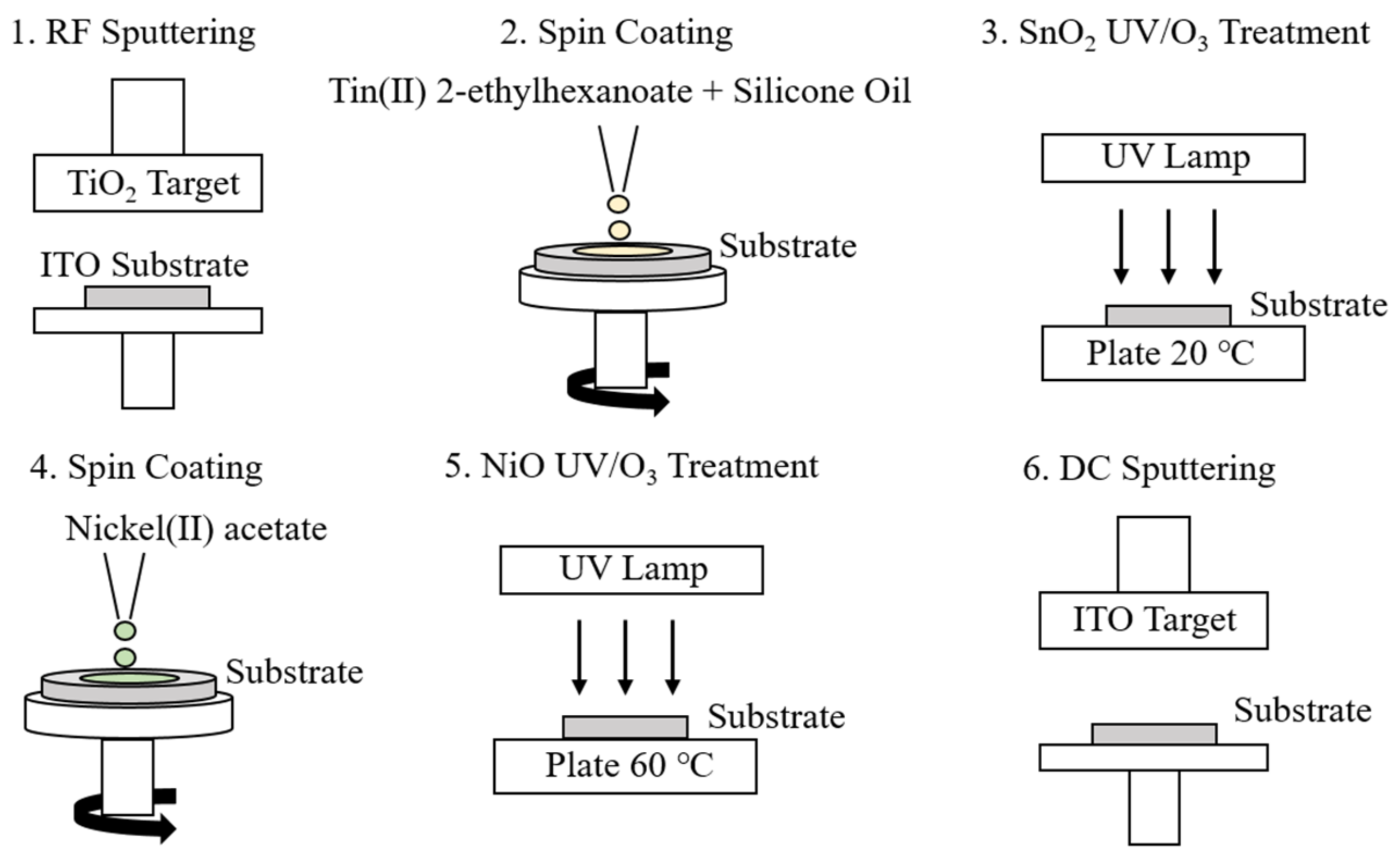
2.1. Fabrication of Sn-Doped NiO Films for Photochromism
2.2. Fabrication of All-Solid-State EC Devices
2.2.1. Spin Coating
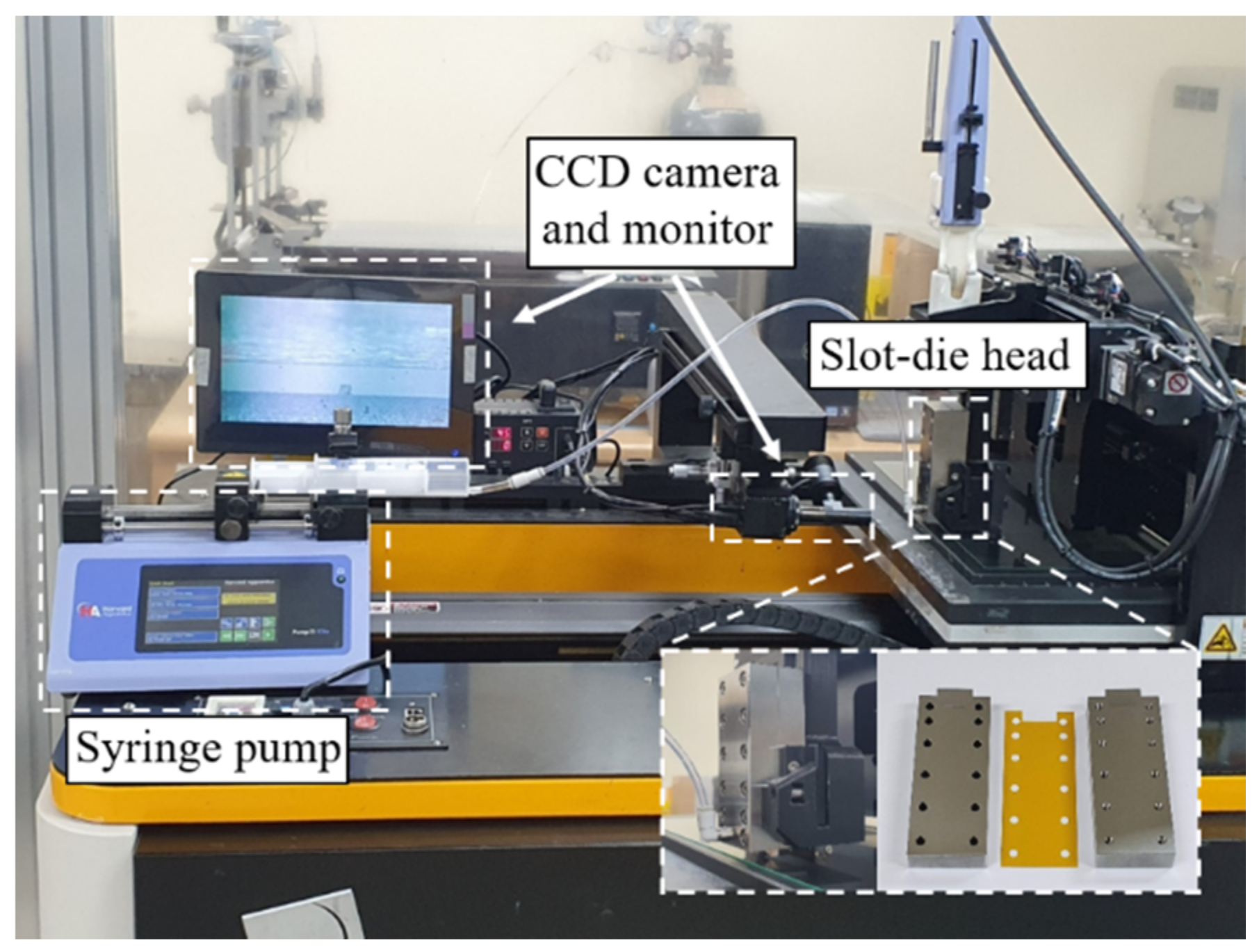
2.2.2. Slot Coating
3. Results
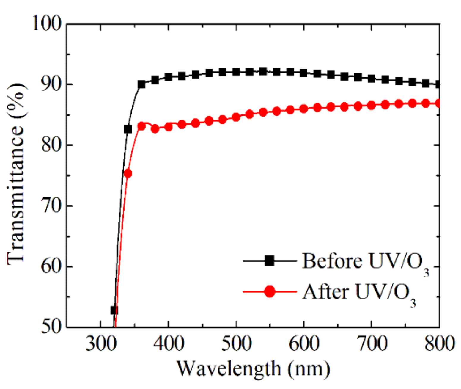
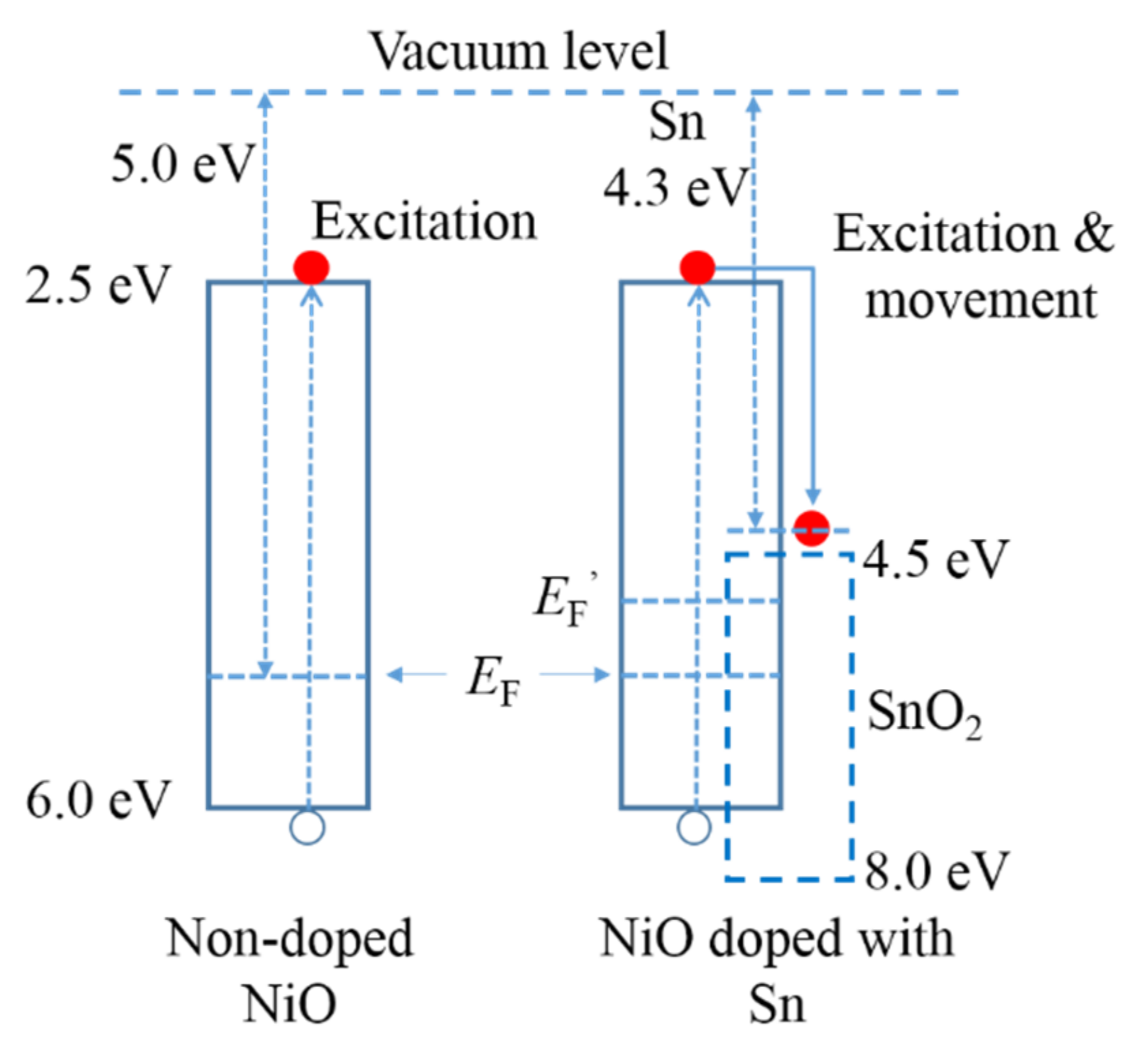
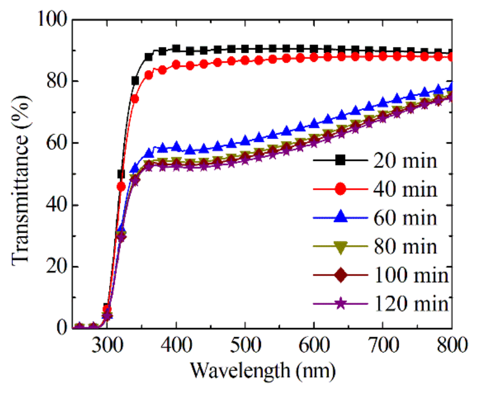
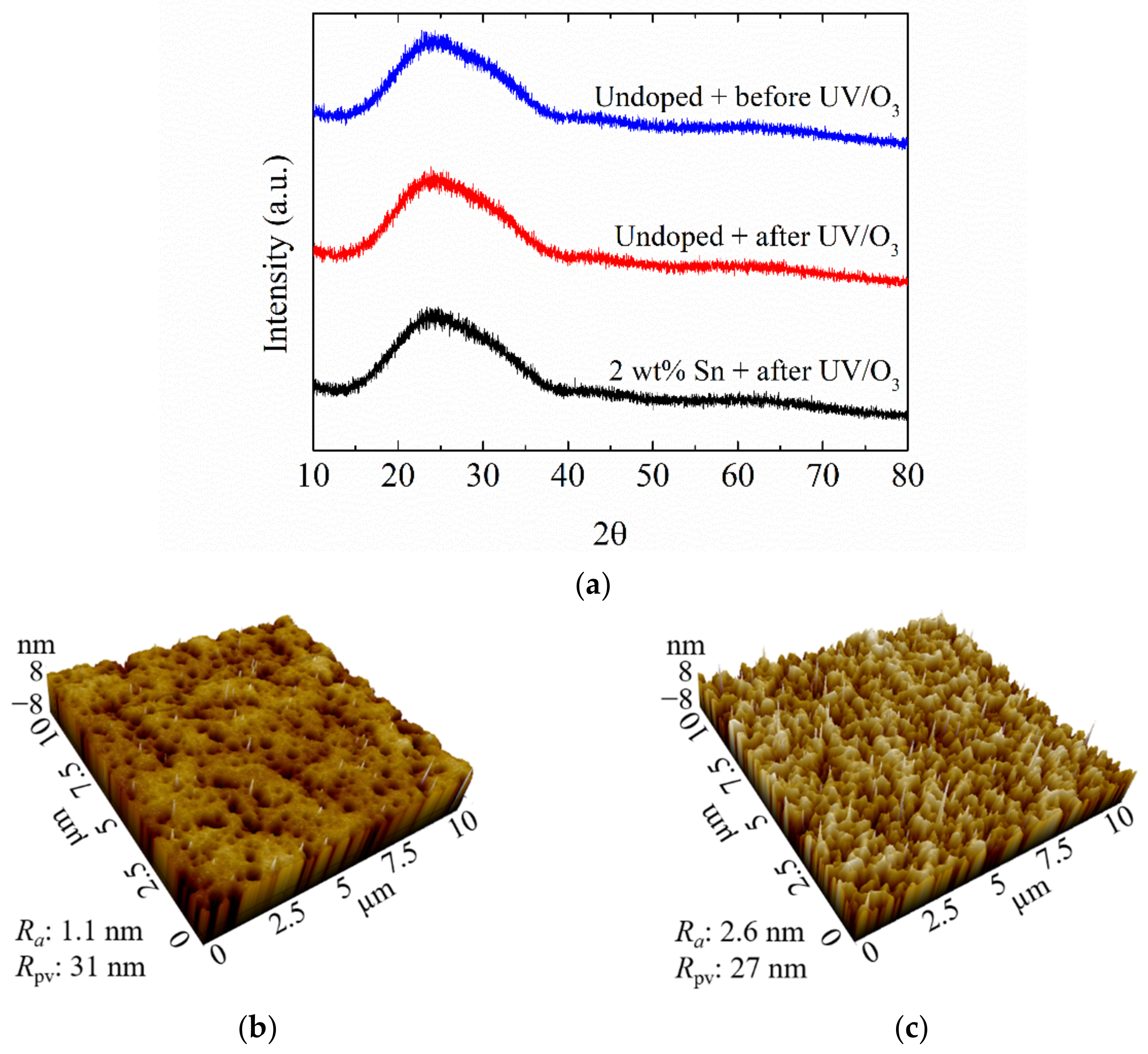
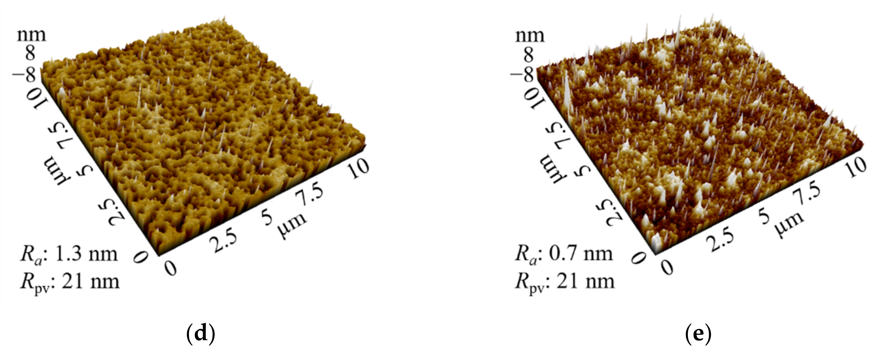
3.1. Photochromic Properties of Sn-Doped NiO Films
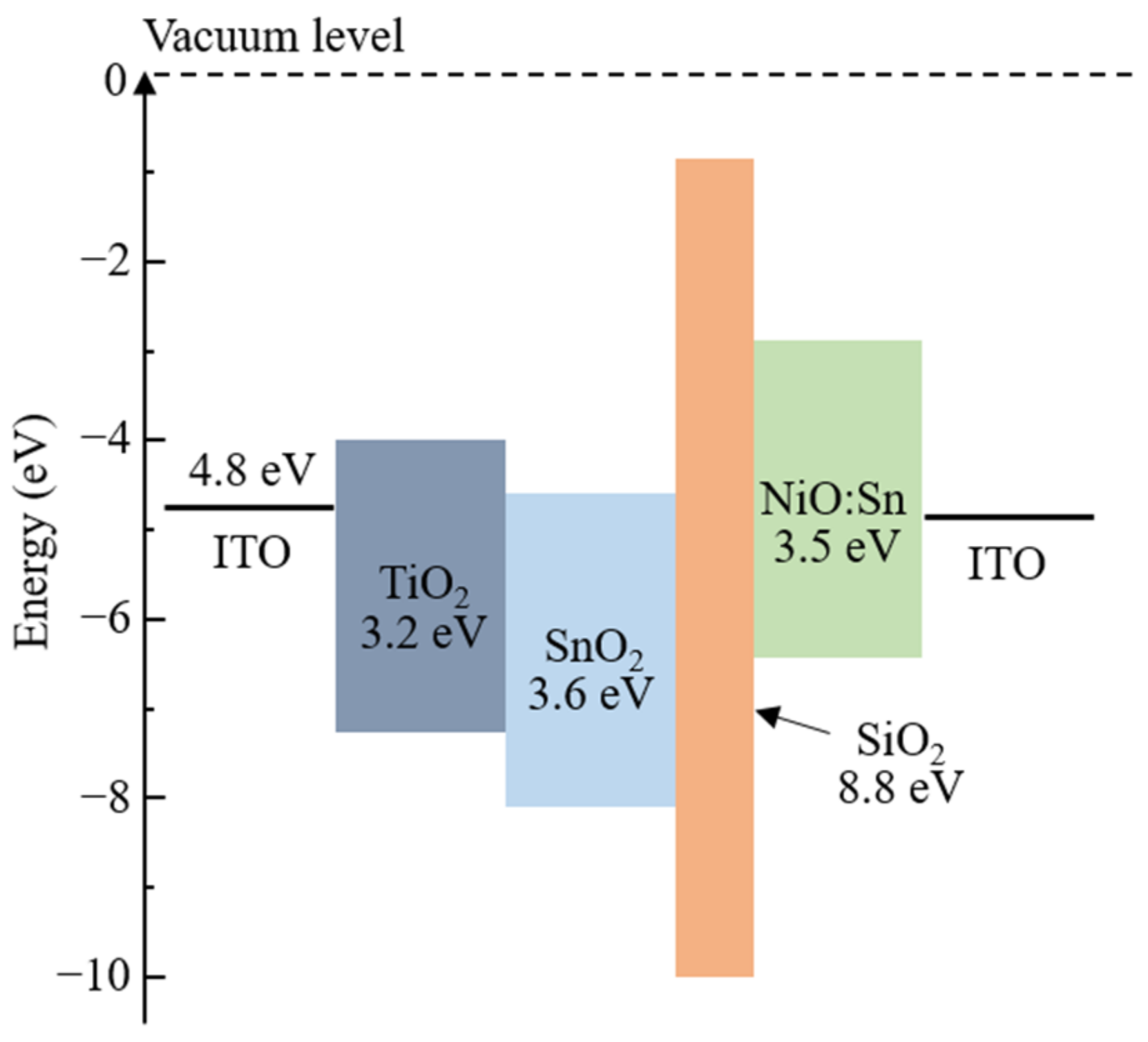
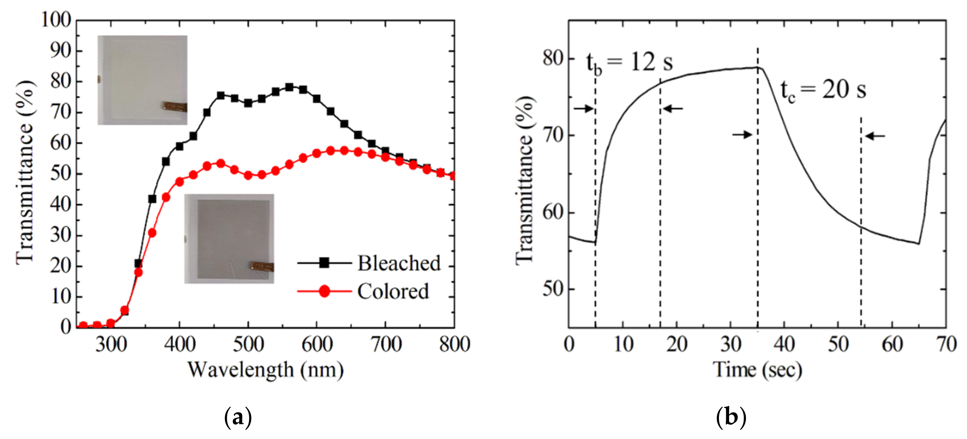
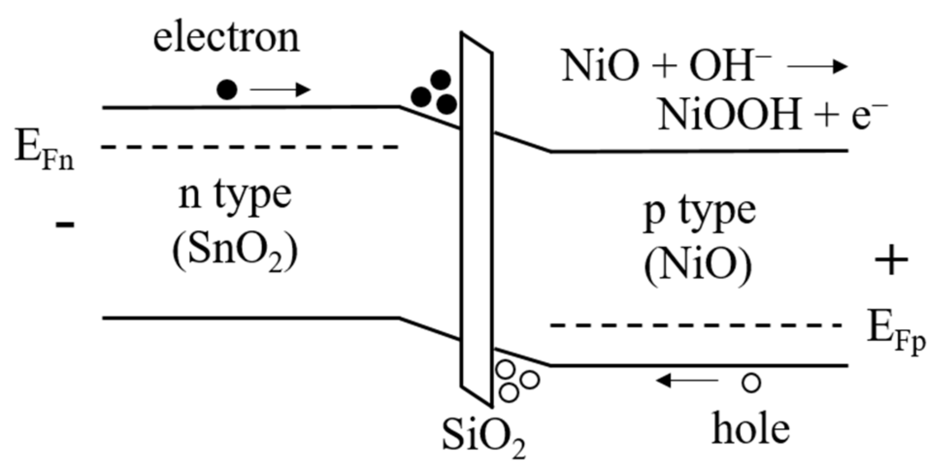
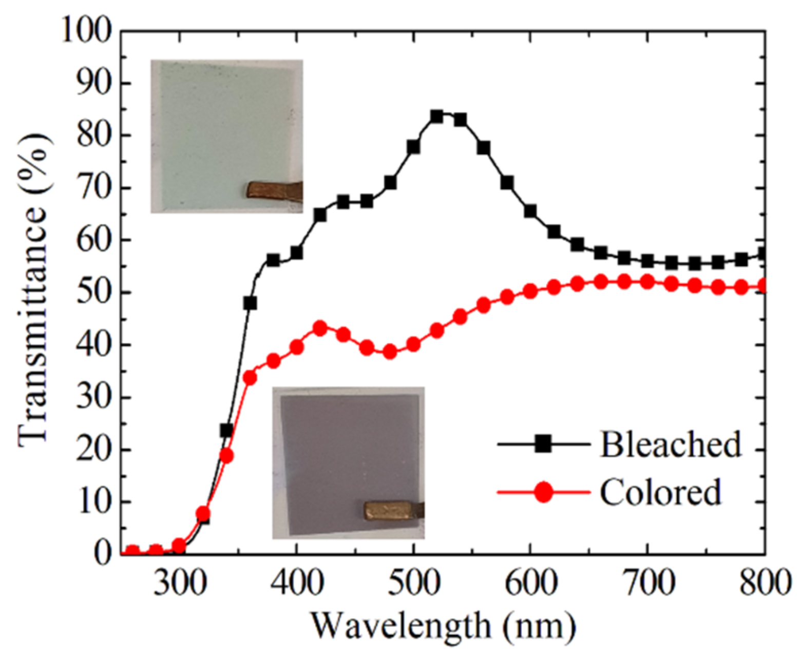
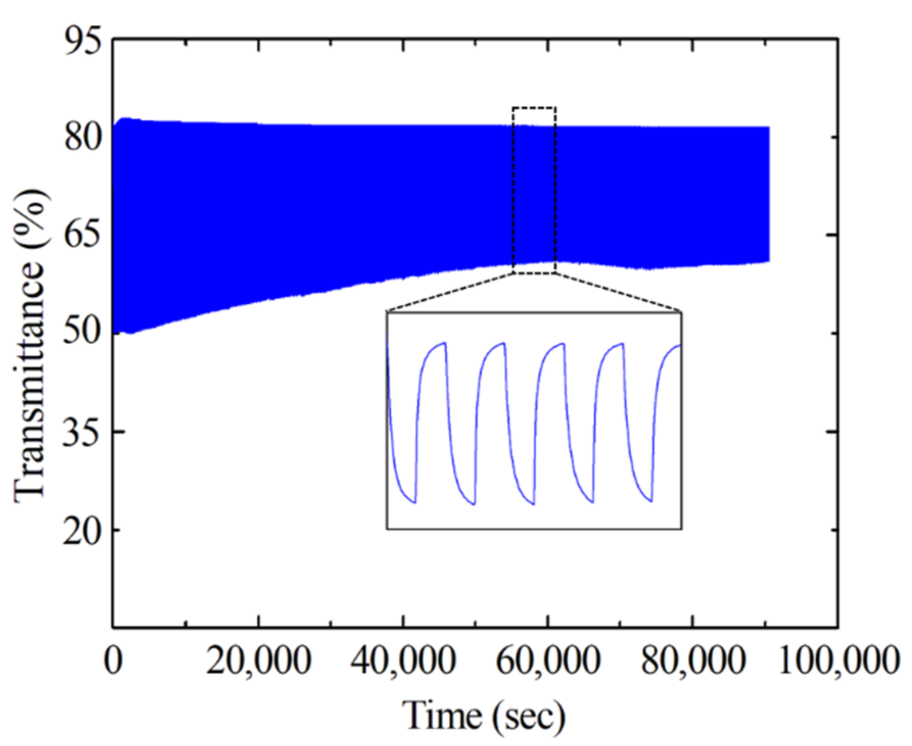
3.2. Electrochromic Properties of EC Devices
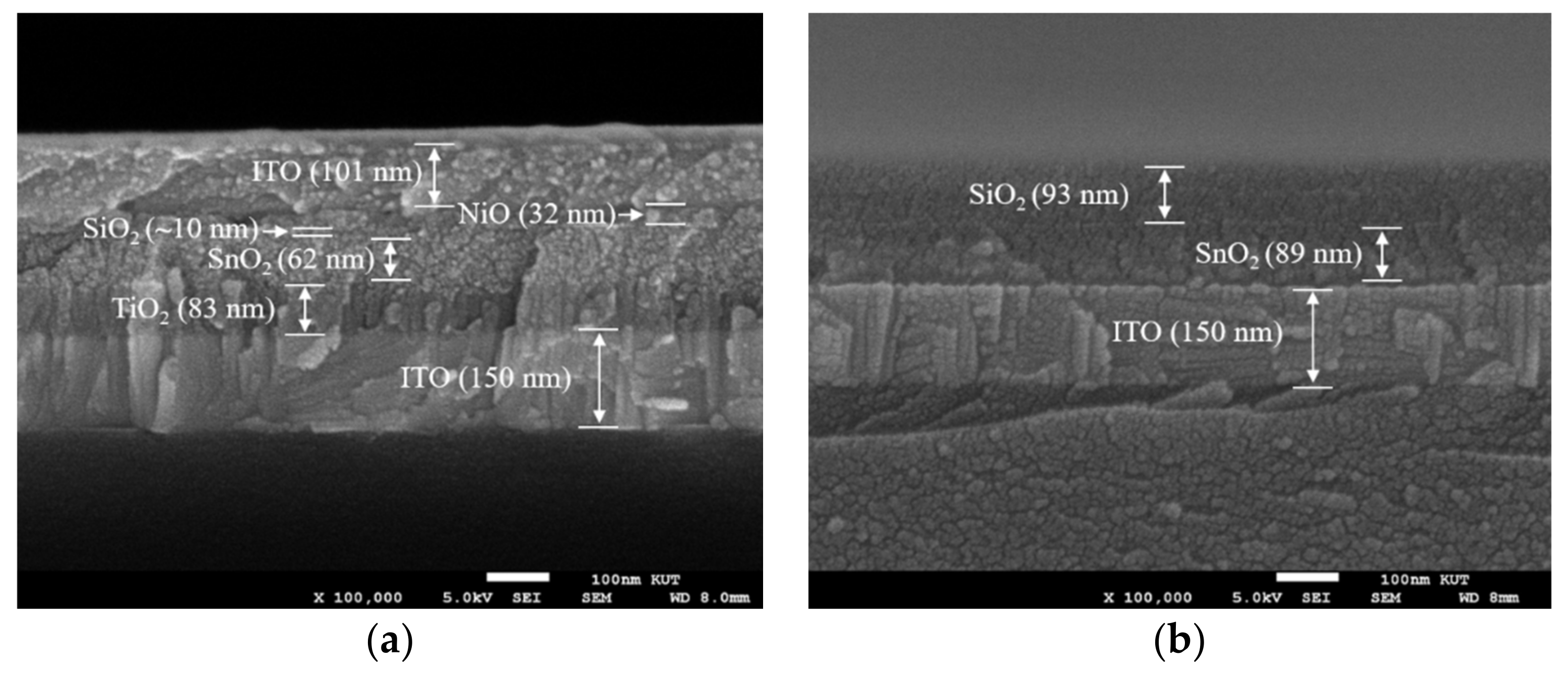
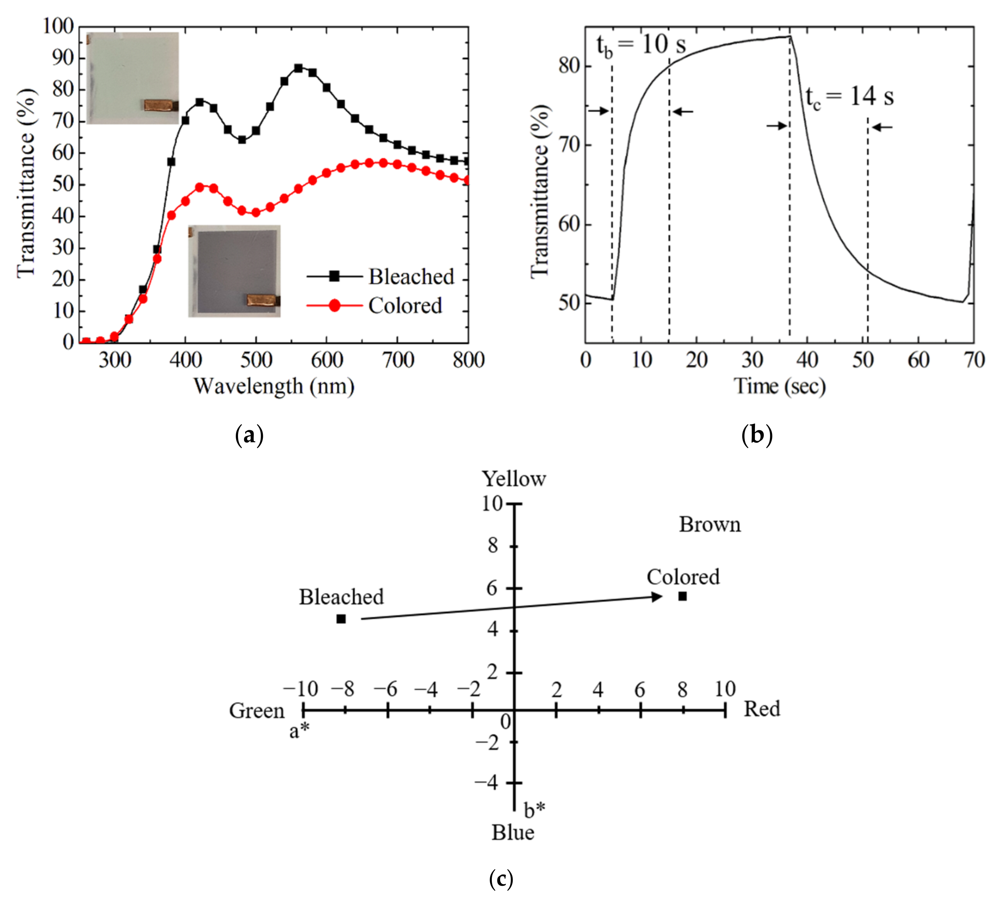
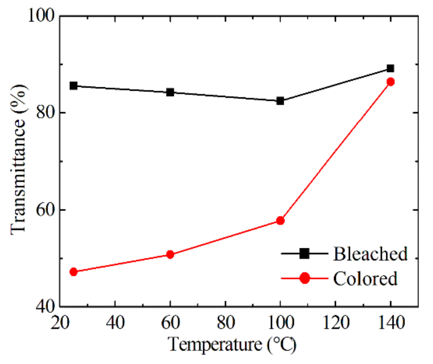
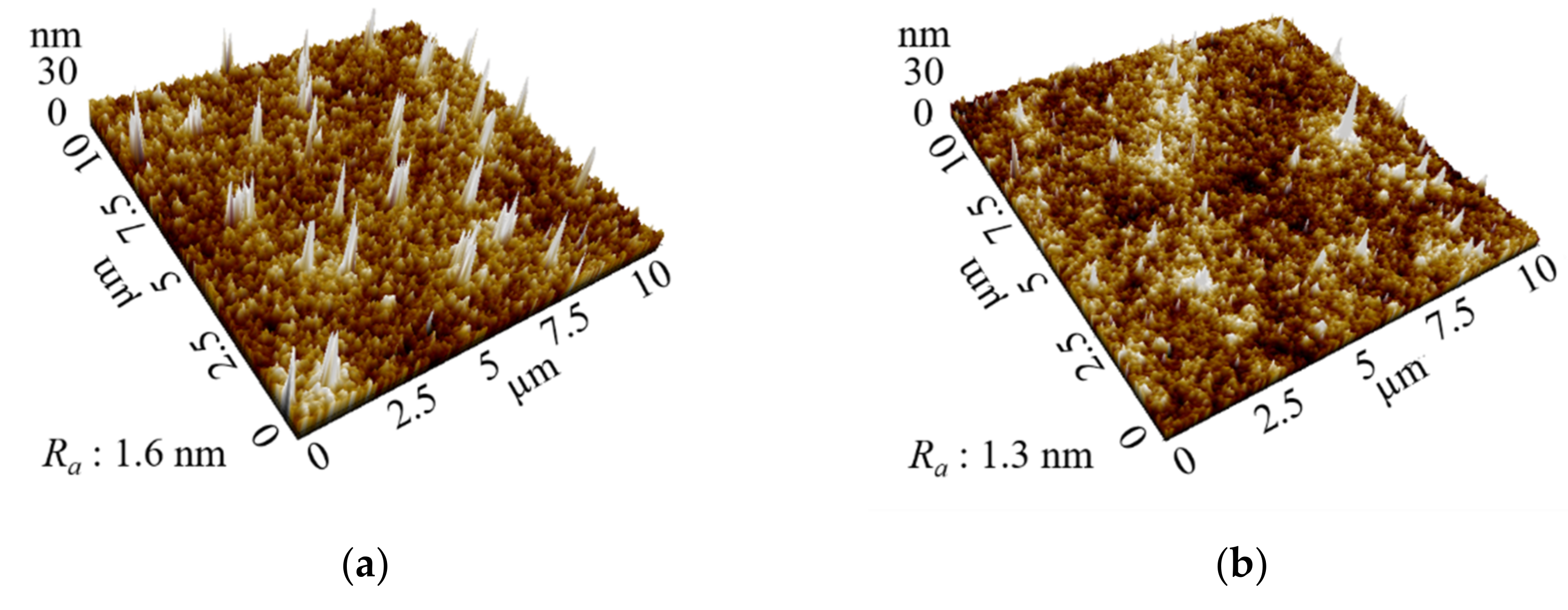
3.3. Comparison between Spin and Slot Coatings
4. Conclusions
Author Contributions
Funding
Institutional Review Board Statement
Informed Consent Statement
Data Availability Statement
Conflicts of Interest
References
- Park, D. Optimization of Nickel Oxide-Based Electrochromic Thin Films. Ph.D. Thesis, Université Sciences et Technologies, Bordeaux, France, 2010. [Google Scholar]
- Ohko, Y.; Tatsuma, T.; Fujii, T.; Naoi, K.; Niwa, C.; Kubota, Y.; Fujishima, A. Multicolour Photochromism of TiO2 Films Loaded with Silver Nanoparticles. Nat. Mater. 2003, 2, 29–31. [Google Scholar] [CrossRef] [PubMed]
- Liptay, W. Electrochromism and Solvatochromism. Angew. Chemie Int. Ed. English 1969, 8, 177–188. [Google Scholar] [CrossRef]
- Li, W.; Zhang, X.; Chen, X.; Zhao, Y.; Wang, L.; Chen, M.; Zhao, J.; Li, Y.; Zhang, Y. Effect of Independently Controllable Electrolyte Ion Content on the Performance of All-Solid-State Electrochromic Devices. Chem. Eng. J. 2020, 398, 125628. [Google Scholar] [CrossRef]
- Patel, K.J.; Bhatt, G.G.; Ray, J.R.; Suryavanshi, P.; Panchal, C.J. All-Inorganic Solid-State Electrochromic Devices: A Review. J. Solid State Electrochem. 2017, 21, 337–347. [Google Scholar] [CrossRef]
- Aegerter, M.; Kim, C.Y. Dip-Coated TiO2 CeO2 Films as Transparent Counter-Electrode for Transmissive Electrochromic Devices Related Papers. J. Non. Cryst. Solids 1990, 121, 319–322. [Google Scholar] [CrossRef] [Green Version]
- Özer, N.; Sabuncu, S.; Cronin, J. Electrochromic Properties of Sol-Gel Deposited Ti-Doped Vanadium Oxide Film. Thin Solid Films 1999, 338, 201–206. [Google Scholar] [CrossRef]
- Azens, A.; Kullman, L.; Vaivars, G.; Nordborg, H.; Granqvist, C.G. Sputter-Deposited Nickel Oxide for Electrochromic Applications. Solid State Ionics 1998, 113–115, 449–456. [Google Scholar] [CrossRef]
- Mehmood, A.; Long, X.; Haidry, A.A.; Zhang, X. Trends in Sputter Deposited Tungsten Oxide Structures for Electrochromic Applications: A Review. Ceram. Int. 2020, 46, 23295–23313. [Google Scholar] [CrossRef]
- Joost, U.; Šutka, A.; Oja, M.; Smits, K.; Döbelin, N.; Loot, A.; Järvekülg, M.; Hirsimäki, M.; Valden, M.; Nõmmiste, E. Reversible Photodoping of TiO2 Nanoparticles for Photochromic Applications. Chem. Mater. 2018, 30, 8968–8974. [Google Scholar] [CrossRef]
- Pittaluga, M. Eco-efficient Materials for Mitigating Building Cooling Needs; Woodhead Publishing: Cambridge, UK, 2015; pp. 473–497. [Google Scholar] [CrossRef]
- Sta, I.; Jlassi, M.; Hajji, M.; Ezzaouia, H. Structural, Optical and Electrical Properties of Undoped and Li-Doped NiO Thin Films Prepared by Sol-Gel Spin Coating Method. Thin Solid Films 2014, 555, 131–137. [Google Scholar] [CrossRef]
- Ren, Y.; Chim, W.K.; Guo, L.; Tanoto, H.; Pan, J.; Chiam, S.Y. The Coloration and Degradation Mechanisms of Electrochromic Nickel Oxide. Sol. Energy Mater. Sol. Cells 2013, 116, 83–88. [Google Scholar] [CrossRef]
- Nundy, S.; Mesloub, A.; Alsolami, B.M.; Ghosh, A. Electrically Actuated Visible and Near-Infrared Regulating Switchable Smart Window for Energy Positive Building: A Review. J. Clean. Prod. 2021, 301, 126854. [Google Scholar] [CrossRef]
- Koo, J.; Amoli, V.; Kim, S.Y.; Lee, C.; Kim, J.; Park, S.M.; Kim, J.; Ahn, J.M.; Jung, K.J.; Kim, D.H. Low-Power, Deformable, Dynamic Multicolor Electrochromic Skin. Nano Energy 2020, 78, 105199. [Google Scholar] [CrossRef]
- Macrelli, G. Optical Characterization of Commercial Large Area Liquid Crystal Devices. Sol. Energy Mater. Sol. Cells 1995, 39, 123–131. [Google Scholar] [CrossRef]
- Piccolo, A.; Pennisi, A.; Simone, F. Daylighting Performance of an Electrochromic Window in a Small Scale Test-Cell. Sol. Energy 2009, 83, 832–844. [Google Scholar] [CrossRef]
- Yang, H.; Wang, C.; Diao, X.; Wang, H.; Wang, T.; Zhu, K. A New All-Thin-Film Electrochromic Device Using LiBSO as the Ion Conducting Layer. J. Phys. D. Appl. Phys. 2008, 41. [Google Scholar] [CrossRef]
- Song, X.; Dong, G.; Gao, F.; Xiao, Y.; Liu, Q.; Diao, X. Properties of NiOx and Its Influence upon All-Thin-Film ITO/NiOx/LiTaO3/WO3/ITO Electrochromic Devices Prepared by Magnetron Sputtering. Vacuum 2015, 111, 48–54. [Google Scholar] [CrossRef]
- Li, W.; Zhang, X.; Chen, X.; Zhao, Y.; Wang, L.; Liu, D.; Li, X.; Chen, M.; Zhao, J.; Li, Y. Preparation and Performance of Fast-Response ITO/Li-NiO/Li-WO3/ITO All-Solid-State Electrochromic Devices by Evaporation Method. Mater. Lett. 2020, 265, 127464. [Google Scholar] [CrossRef]
- Yoshimura, H.; Koshida, N. Fast Electrochromic Effect Obtained from Solid-State Inorganic Thin-Film Configuration with a Carrier Accumulation Structure. Appl. Phys. Lett. 2006, 88, 86–89. [Google Scholar] [CrossRef]
- Wang, S.C.; Liu, K.Y.; Huang, J.L. Tantalum Oxide Film Prepared by Reactive Magnetron Sputtering Deposition for All-Solid-State Electrochromic Device. Thin Solid Films 2011, 520, 1454–1459. [Google Scholar] [CrossRef]
- Kim, K.H.; Kahuku, M.; Abe, Y.; Kawamura, M.; Kiba, T. Improved Electrochromic Performance in Nickel Oxide Thin Film by Zn Doping. Int. J. Electrochem. Sci. 2020, 15, 4065–4071. [Google Scholar] [CrossRef]
- Patil, P.S.; Sadale, S.B.; Mujawar, S.H.; Shinde, P.S.; Chigare, P.S. Synthesis of Electrochromic Tin Oxide Thin Films with Faster Response by Spray Pyrolysis. Appl. Surf. Sci. 2007, 253, 8560–8567. [Google Scholar] [CrossRef]
- Azevedo, C.F.; Balboni, R.D.C.; Cholant, C.M.; Moura, E.A.; Lemos, R.M.J.; Pawlicka, A.; Gündel, A.; Flores, W.H.; Pereira, M.; Avellaneda, C.O. New Thin Films of NiO Doped with V2O5 for Electrochromic Applications. J. Phys. Chem. Solids 2017, 110, 30–35. [Google Scholar] [CrossRef]
- Takaki, H.; Inoue, S.; Matsumura, Y. Requirements for Photochromism in Double-Layer Metal Oxide Films. Chem. Phys. Lett. 2019, 732, 136620. [Google Scholar] [CrossRef]
- Wang, K.; Zhang, H.; Xie, W.; Chen, G.; Jiang, R.; Tao, K.; Liang, L.; Gao, J.; Cao, H. Unraveling the Role of Water on the Electrochromic and Electrochemical Properties of Nickel Oxide Electrodes in Electrochromic Pseudocapacitors. J. Electrochem. Soc. 2021, 168, 113502. [Google Scholar] [CrossRef]
- Sawaby, A.; Selim, M.S.; Marzouk, S.Y.; Mostafa, M.A.; Hosny, A. Structure, Optical and Electrochromic Properties of NiO Thin Films. Phys. B Condens. Matter 2010, 405, 3412–3420. [Google Scholar] [CrossRef]
- Tachikawa, H.; Abe, S. Spectral Shifts of Ozone Molecule by the Complex Formation with a Water Molecule. Chem. Phys. Lett. 2006, 432, 409–413. [Google Scholar] [CrossRef]
- Noonuruk, R.; Wongpisutpaisan, N.; Mukdacharoenchai, P.; Techitdheera, W.; Pecharapa, W. Ozone-Induced Optical Density Change of NiO Thin Films and Their Applicability as Neutral Optical Density Filter. Procedia Eng. 2011, 8, 212–216. [Google Scholar] [CrossRef]
- Méndez, P.F.; Muhammed, S.K.M.; Barea, E.M.; Masi, S.; Mora-Seró, I. Analysis of the UV–Ozone-Treated SnO2 Electron Transporting Layer in Planar Perovskite Solar Cells for High Performance and Reduced Hysteresis. Sol. RRL 2019, 3, 1–6. [Google Scholar] [CrossRef]
- Wang, K.; Qiu, D.; Zhang, H.; Chen, G.; Xie, W.; Tao, K.; Bao, S.; Liang, L.; Gao, J.; Cao, H. Boosting Charge-Transfer Kinetics and Cyclic Stability of Complementary WO3–NiO Electrochromic Devices via SnOx Interfacial Layer. J. Sci. Adv. Mater. Devices 2021, 6, 494–500. [Google Scholar] [CrossRef]
- Lin, T.; Li, X.; Jang, J. High Performance P-Type NiOx Thin-Film Transistor by Sn Doping. Appl. Phys. Lett. 2016, 108. [Google Scholar] [CrossRef]
- Ouyang, M.; Yuan, C.; Muisener, R.J.; Boulares, A.; Koberstein, J.T. Conversion of Some Siloxane Polymers to Silicon Oxide by UV/Ozone Photochemical Processes. Chem. Mater. 2000, 12, 1591–1596. [Google Scholar] [CrossRef]
- Shi, J.; Lai, L.; Zhang, P.; Li, H.; Qin, Y.; Gao, Y.; Luo, L.; Lu, J. Aluminum Doped Nickel Oxide Thin Film with Improved Electrochromic Performance from Layered Double Hydroxides Precursor in Situ Pyrolytic Route. J. Solid State Chem. 2016, 241, 1–8. [Google Scholar] [CrossRef]
- Jung, K.; Kim, D.H.; Kim, J.; Ko, S.; Choi, J.W.; Kim, K.C.; Lee, S.G.; Lee, M.J. Influence of a UV-Ozone Treatment on Amorphous SnO2 Electron Selective Layers for Highly Efficient Planar MAPbI3 Perovskite Solar Cells. J. Mater. Sci. Technol. 2020, 59, 195–202. [Google Scholar] [CrossRef]


| Sn Concentration (wt%) | ∆T (%) |
|---|---|
| Non-doped | 5.1 |
| 1 | 20.5 |
| 2 | 25.7 |
| 3 | 21.0 |
| TiO2 Thickness (nm) | ∆T (%) |
|---|---|
| 95 | 21.3 |
| 83 | 25.7 |
| 63 | 26.9 |
| 48 | 38.3 |
| 32 | 23.1 |
| 16 | 15.4 |
| Silicone Oil Concentration (wt%) | ∆T (%) |
|---|---|
| 0 | 4.4 |
| 1 | 8.4 |
| 2 | 32.9 |
| 3 | 38.3 |
| 4 | 31.5 |
| Layer | Spin Coating | Slot Coating | ||
|---|---|---|---|---|
| Rpv (nm) | Ra (nm) | Rpv (nm) | Ra (nm) | |
| SnO2 | 43 | 1.6 | 16 | 0.9 |
| NiO | 32 | 1.3 | 15 | 0.6 |
Publisher’s Note: MDPI stays neutral with regard to jurisdictional claims in published maps and institutional affiliations. |
© 2021 by the authors. Licensee MDPI, Basel, Switzerland. This article is an open access article distributed under the terms and conditions of the Creative Commons Attribution (CC BY) license (https://creativecommons.org/licenses/by/4.0/).
Share and Cite
Kim, G.; Hong, S.; Yoo, S.; Park, J. Solution-Processed All-Solid-State Electrochromic Devices Based on SnO2/NiO doped with Tin. Coatings 2021, 11, 1431. https://doi.org/10.3390/coatings11111431
Kim G, Hong S, Yoo S, Park J. Solution-Processed All-Solid-State Electrochromic Devices Based on SnO2/NiO doped with Tin. Coatings. 2021; 11(11):1431. https://doi.org/10.3390/coatings11111431
Chicago/Turabian StyleKim, Gieun, Songeun Hong, Suho Yoo, and Jongwoon Park. 2021. "Solution-Processed All-Solid-State Electrochromic Devices Based on SnO2/NiO doped with Tin" Coatings 11, no. 11: 1431. https://doi.org/10.3390/coatings11111431
APA StyleKim, G., Hong, S., Yoo, S., & Park, J. (2021). Solution-Processed All-Solid-State Electrochromic Devices Based on SnO2/NiO doped with Tin. Coatings, 11(11), 1431. https://doi.org/10.3390/coatings11111431