
Large Negative Photoresistivity in Amorphous NdNiO3 Film

 , ,
, ,  and
and 
Abstract
:1. Introduction
2. Materials and Methods
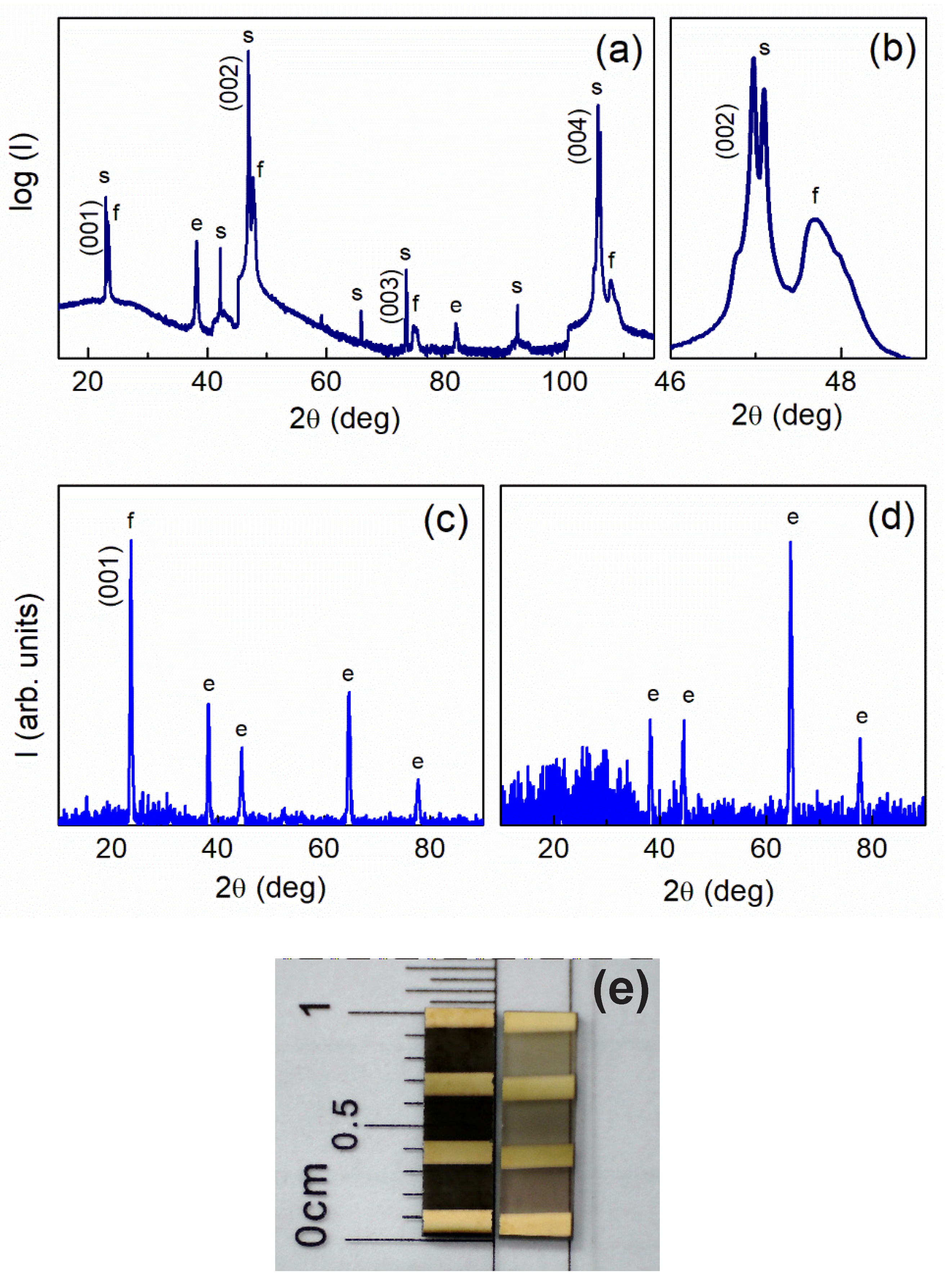
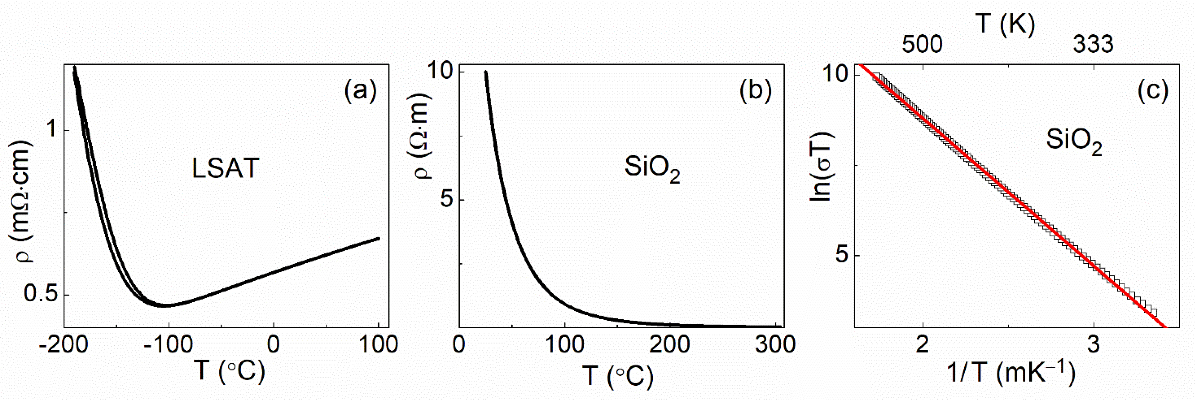
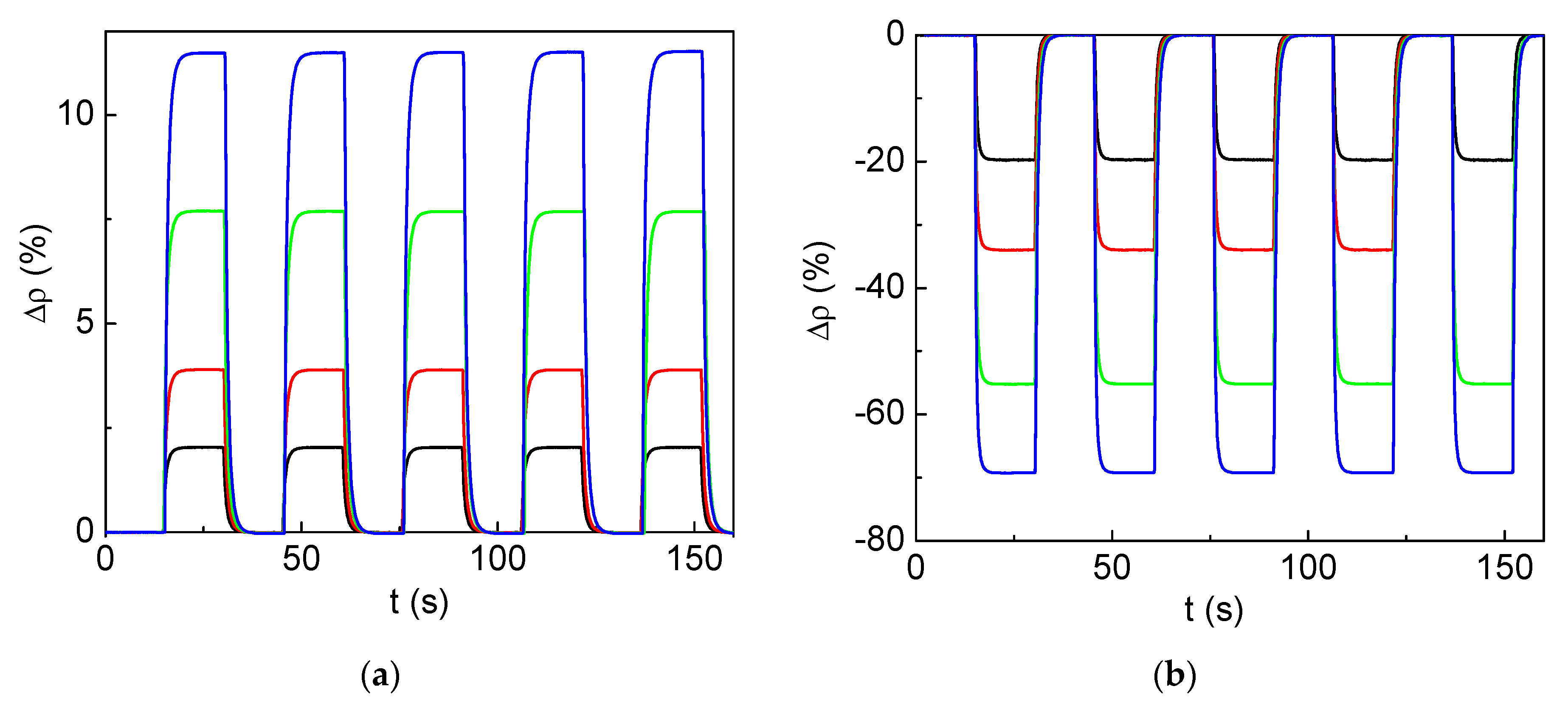
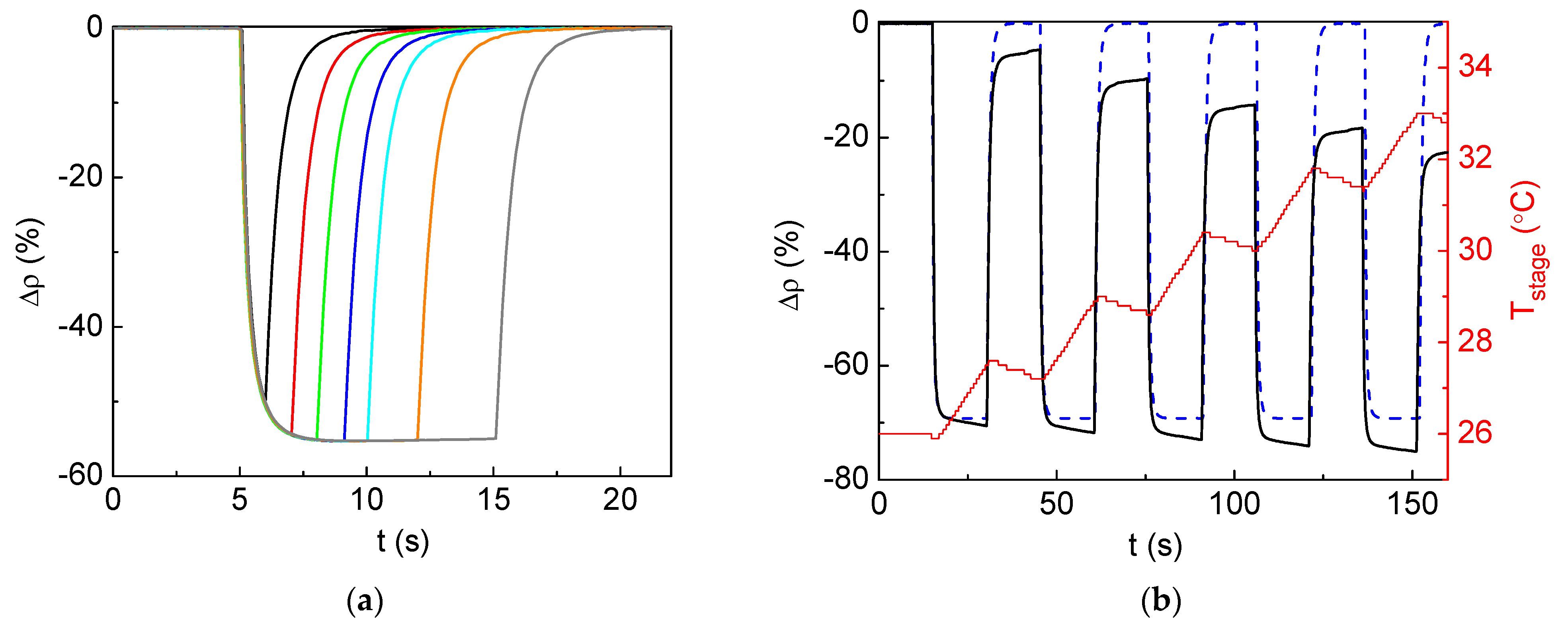
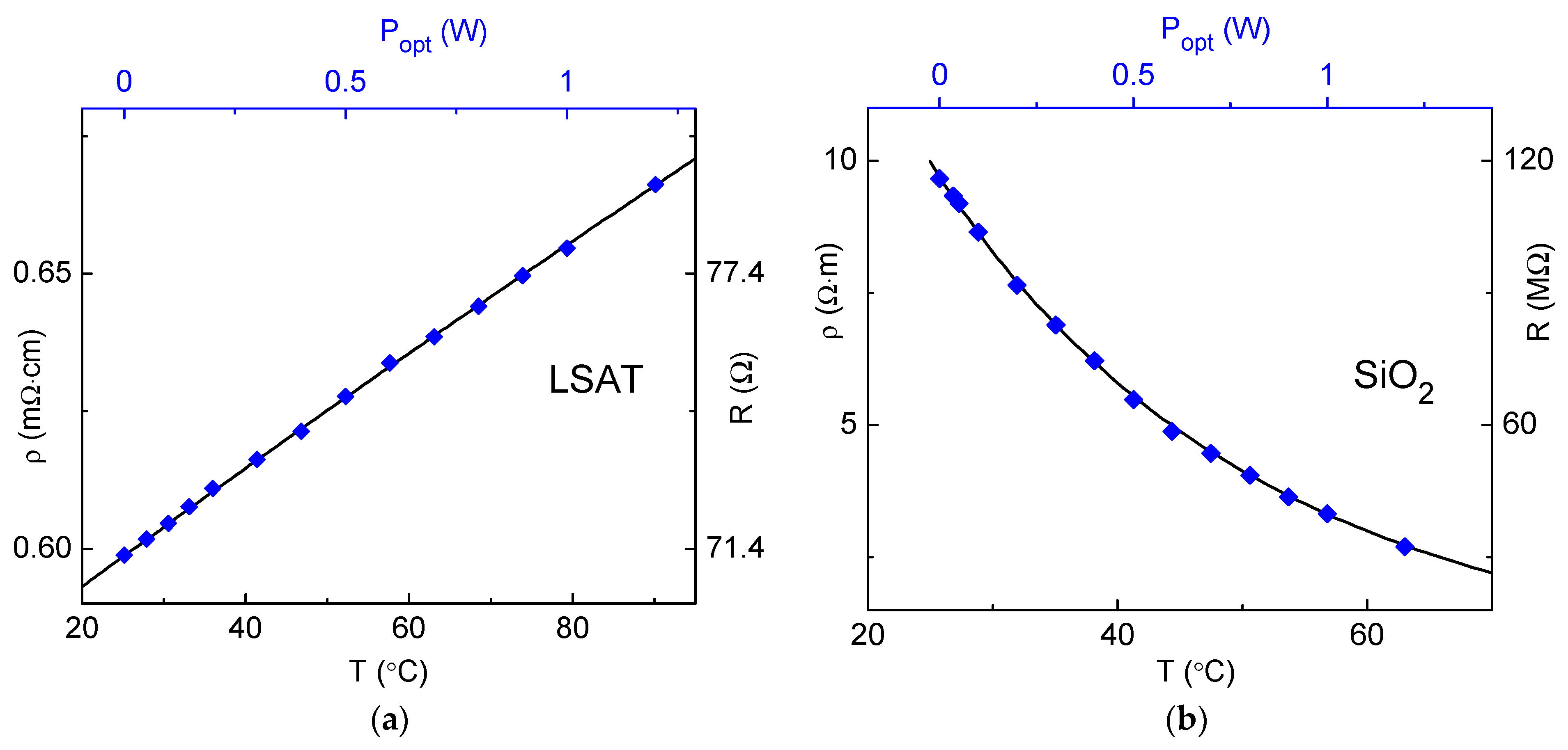
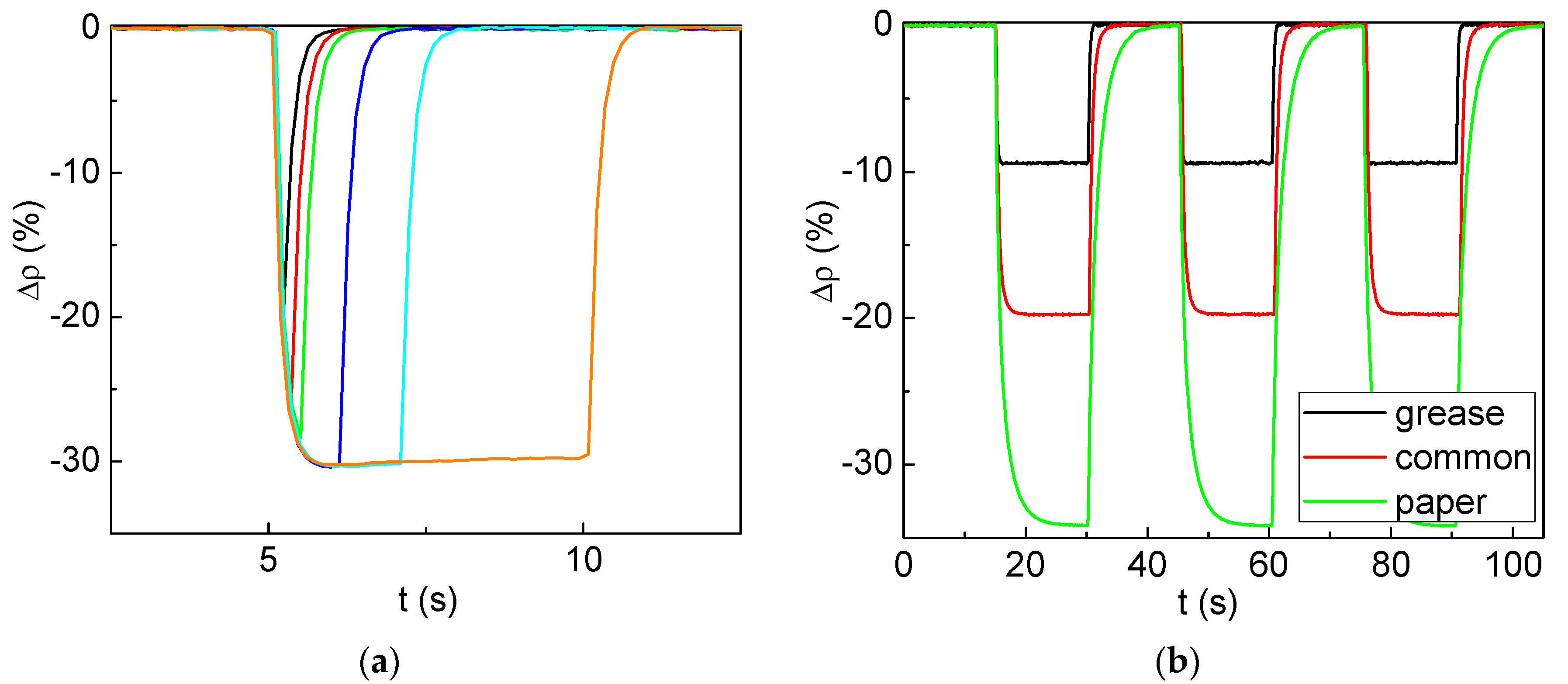
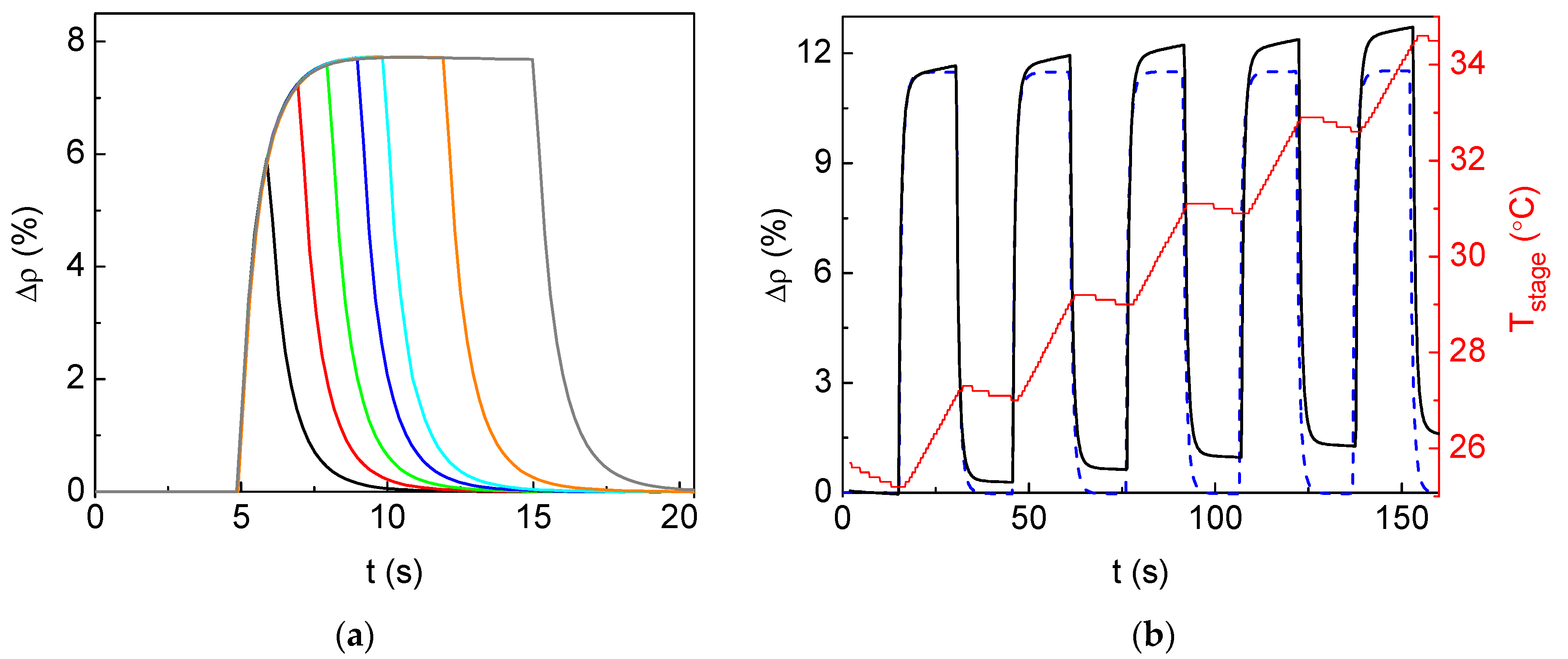
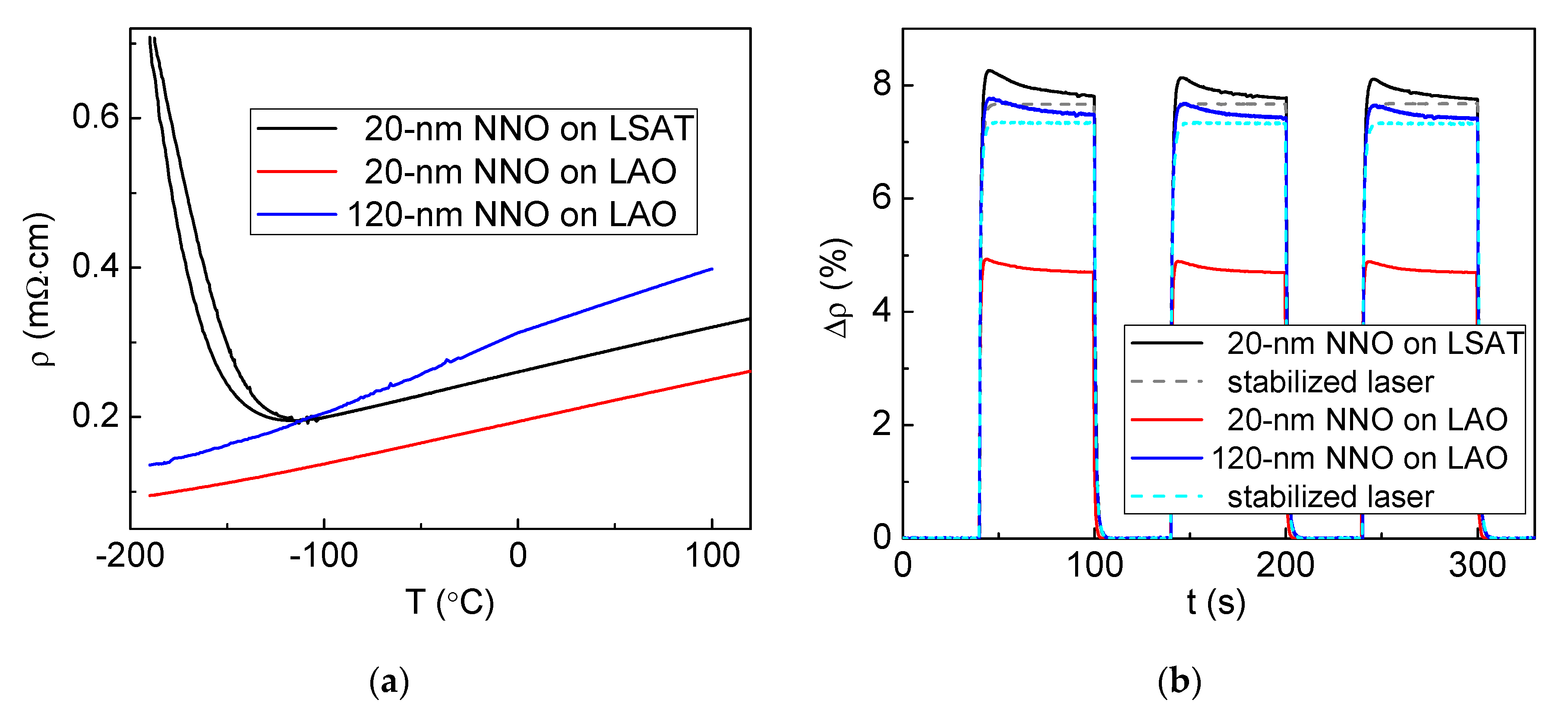
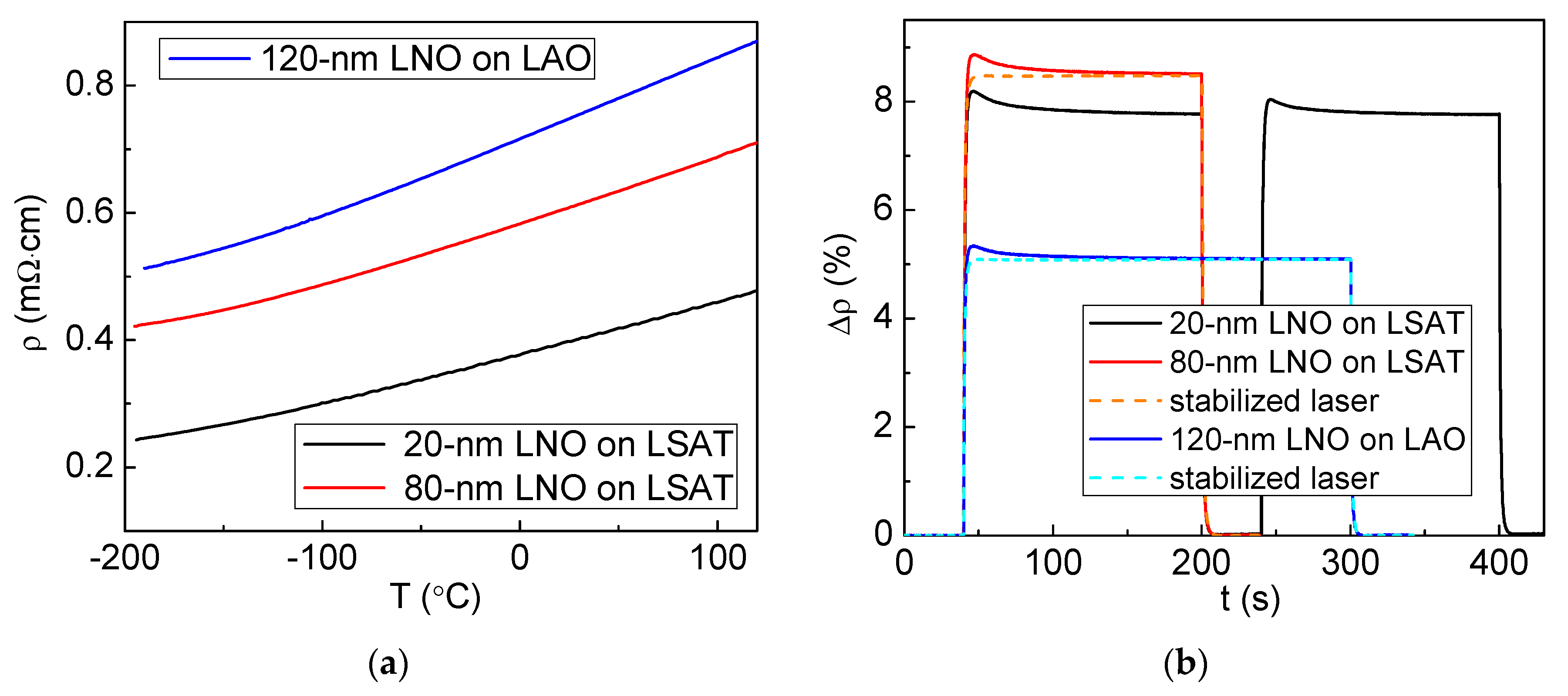
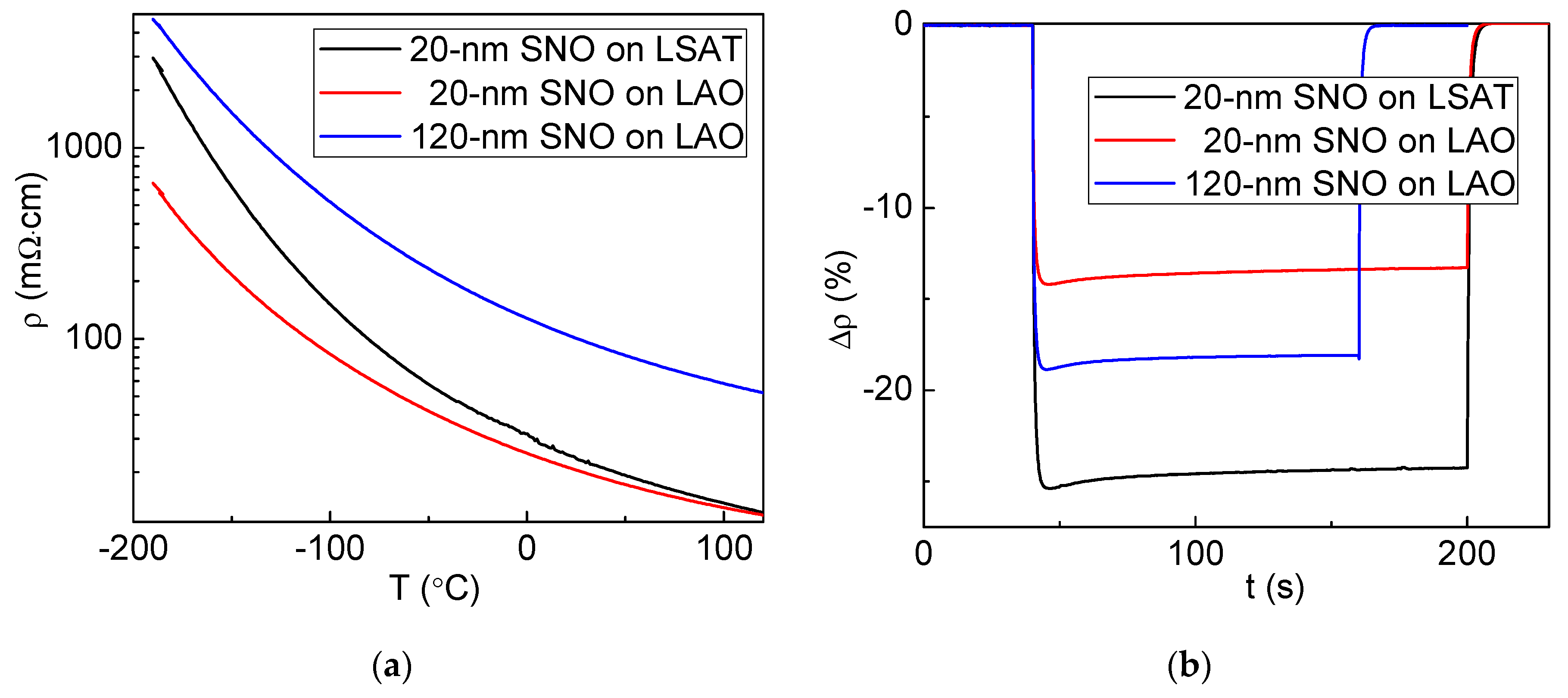
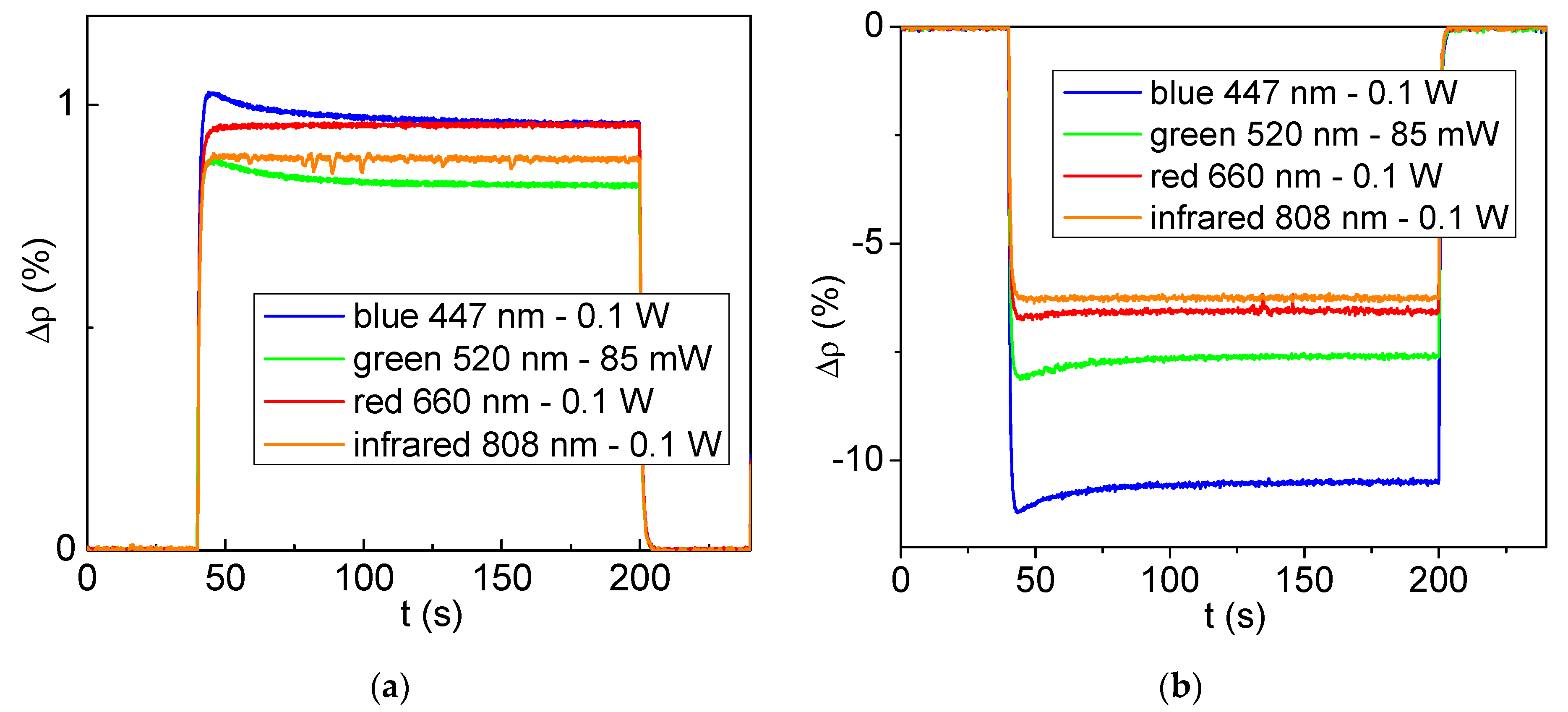
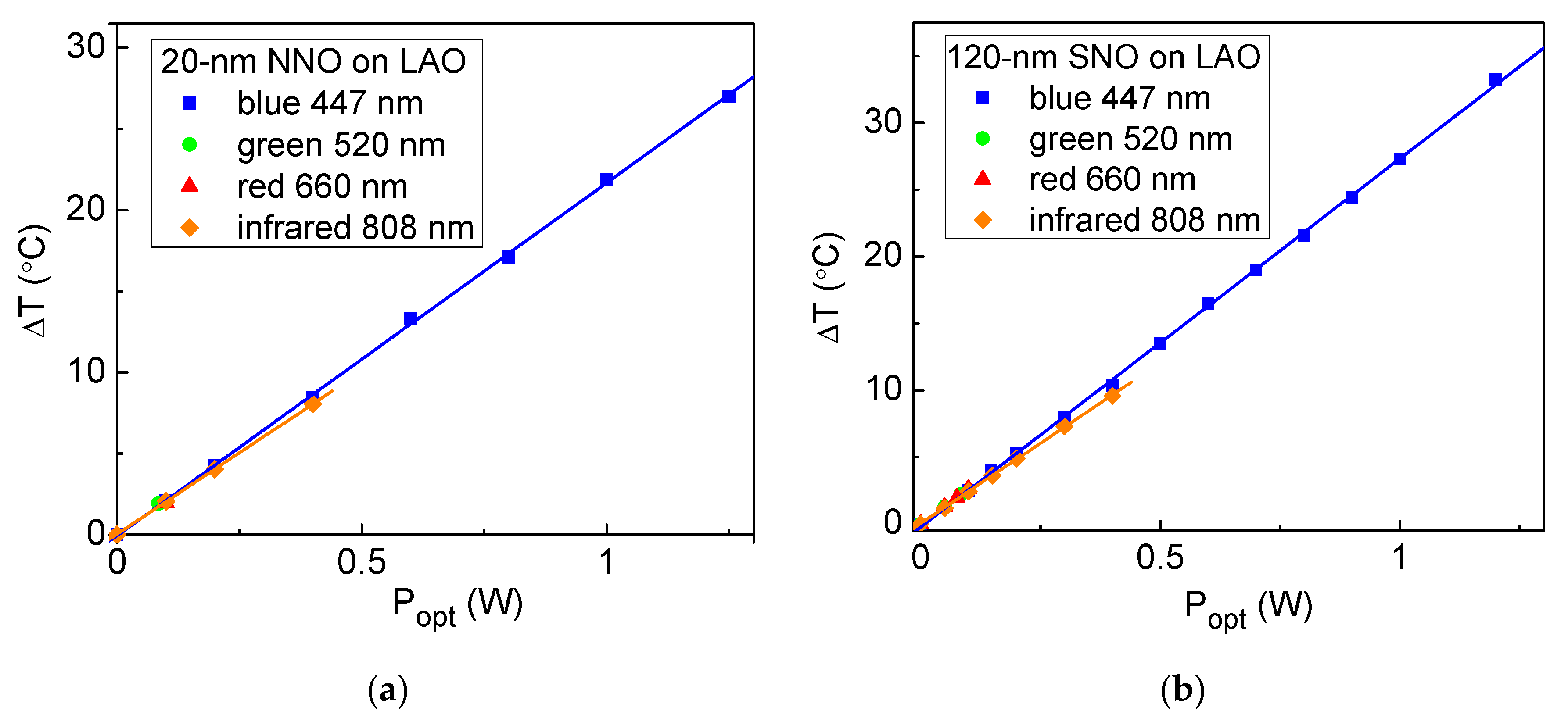
3. Results
4. Discussion
5. Conclusions
Author Contributions
Funding
Institutional Review Board Statement
Informed Consent Statement
Data Availability Statement
Conflicts of Interest
Appendix A


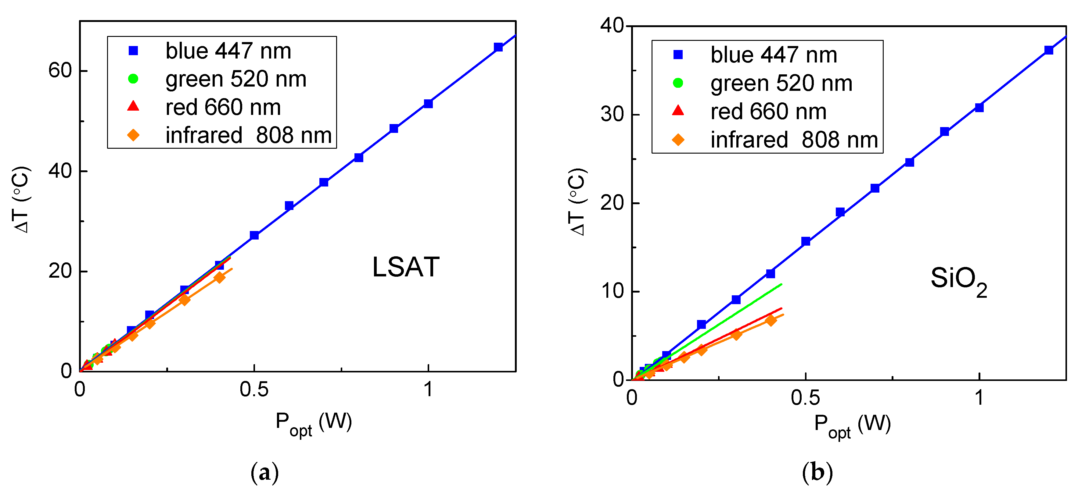
| Film | NNO | LNO | SNO | ||||||||
|---|---|---|---|---|---|---|---|---|---|---|---|
| Substrate | LSAT | LAO | SiO2 | LSAT | LAO | LSAT | LAO | ||||
| Thickness, nm | 20 | 80 | 20 | 120 | 80 | 20 | 80 | 120 | 20 | 20 | 120 |
| Δρ, % | 7.7 | 7.7 | 4.7 | 7.4 | −55 | 7.8 | 8.5 | 5.1 | −24 | −13.4 | −18 |
| α, % | 83.7 | 91.8 | 77.2 | 96.5 | 52.8 | 79.8 | 92 | 96.2 | 80.3 | 71.9 | 86 |
| ρ, mΩ·cm | 0.277 | 0.6 | 0.21 | 0.34 | 106 | 0.4 | 0.61 | 0.76 | 25.2 | 22.3 | 99.5 |
| dρ/dT, µΩ·cm/K | 0.61 | 1.1 | 0.57 | 0.88 | −36·106 | 0.88 | 1 | 1.3 | −231 | −172 | −731 |
| ΔT, °C | 36 | 42.7 | 17 | 29 | 25 | 35 | 50 | 30 | 35 | 20 | 25 |
References
- Park, J.; Lim, Y.; Kong, S.; Lee, H.; Kim, Y.-B. Rapid fabrication of chemical solution-deposited lanthanum nickelate thin films via intense pulsed-light process. Coatings 2019, 9, 372. [Google Scholar] [CrossRef] [Green Version]
- Medarde, M.L. Structural, magnetic and electronic properties of RNiO3 perovskites (R = rare earth). J. Phys. Condens. Matter. 1997, 9, 1679–1707. [Google Scholar] [CrossRef]
- Catalan, G. Progress in perovskite nickelate research. Phase Transit. 2008, 81, 729–749. [Google Scholar] [CrossRef]
- Middey, S.; Chakhalian, J.; Mahadevan, P.; Freeland, J.W.; Millis, A.J.; Sarma, D.D. Physics of ultrathin films and heterostructures of rare-earth nickelates. Annu. Rev. Mater. Res. 2016, 46, 305–334. [Google Scholar] [CrossRef] [Green Version]
- Catalano, S.; Gibert, M.; Fowlie, J.; Íñiguez, J.; Triscone, J.-M.; Kreisel, J. Rare-earth nickelates RNiO3: Thin films and heterostructures. Rep. Prog. Phys. 2018, 81, 046501. [Google Scholar] [CrossRef] [PubMed] [Green Version]
- Liu, J.; Kargarian, M.; Kareev, M.; Gray, B.; Ryan, P.J.; Cruz, A.; Tahir, N.; Chuang, Y.D.; Guo, J.; Rondinelli, J.M.; et al. Heterointerface engineered electronic and magnetic phases of NdNiO3 thin films. Nat. Commun. 2013, 4, 2714. [Google Scholar] [CrossRef] [PubMed] [Green Version]
- Wang, L.; Ju, S.; You, L.; Qi, Y.; Guo, Y.; Ren, P.; Zhou, Y.; Wang, J. Competition between strain and dimensionality effects on the electronic phase transitions in NdNiO3 films. Sci. Rep. 2015, 5, 18707. [Google Scholar] [CrossRef] [PubMed] [Green Version]
- Mikheev, E.; Hauser, A.J.; Himmetoglu, B.; Moreno, N.E.; Janotti, A.; Van de Walle, C.G.; Stemmer, S. Tuning bad metal and non-Fermi liquid behavior in a Mott material: Rare-earth nickelate thin films. Sci. Adv. 2015, 1, e1500797. [Google Scholar] [CrossRef] [PubMed] [Green Version]
- Stupakov, A.; Pacherova, O.; Kocourek, T.; Jelinek, M.; Dejneka, A.; Tyunina, M. Negative magnetoresistance in epitaxial films of neodymium nickelate. Phys. Rev. B 2019, 99, 085111. [Google Scholar] [CrossRef] [Green Version]
- Liao, Z.; Gauquelin, N.; Green, R.J.; Müller-Caspary, K.; Lobato, I.; Li, L.; Van Aert, S.; Verbeeck, J.; Huijben, M.; Grisolia, M.N.; et al. Metal–insulator-transition engineering by modulation tilt-control in perovskite nickelates for room temperature optical switching. Proc. Natl. Acad. Sci. USA 2018, 115, 9515–9520. [Google Scholar] [CrossRef] [Green Version]
- Ahn, C.; Cavalleri, A.; Georges, A.; Ismail-Beigi, C.; Millis, A.J.; Triscone, J.-M. Designing and controlling the properties of transition metal oxide quantum materials. Nat. Mater. 2021, 20, 1462–1468. [Google Scholar] [CrossRef]
- Mattoni, G.; Manca, N.; Hadjimichael, M.; Zubko, P.; van der Torren, A.J.; Yin, C.; Catalano, S.; Gibert, M.; Maccherozzi, F.; Liu, Y.; et al. Light control of the nanoscale phase separation in heteroepitaxial nickelates. Phys. Rev. Mater. 2018, 2, 085002. [Google Scholar] [CrossRef] [Green Version]
- Chen, B.; Gauquelin, N.; Jannis, D.; Cunha, D.M.; Halisdemir, U.; Piamonteze, C.; Lee, J.H.; Belhadi, J.; Eltes, F.; Abel, S.; et al. Strain-engineered metal-to-insulator transition and orbital polarization in nickelate superlattices integrated on silicon. Adv. Mater. 2020, 32, 2004995. [Google Scholar] [CrossRef]
- Sun, Y.; Wang, Q.; Park, T.J.; Gage, T.E.; Zhang, Z.; Wang, X.; Zhang, D.; Sun, X.; He, J.; Zhou, H.; et al. Electrochromic properties of perovskite NdNiO3 thin films for smart windows. ACS Appl. Electron. Mater. 2021, 3, 1719–1731. [Google Scholar] [CrossRef]
- Lin, T.-K.; Chang, H.-W.; Chou, W.-C.; Wang, C.-R.; Wei, D.-H.; Tu, C.-S.; Chen, P.-Y. Multiferroic and nanomechanical properties of Bi1-xGdxFeO3 polycrystalline films (x = 0.00–0.15). Coatings 2021, 11, 900. [Google Scholar] [CrossRef]
- Thiruchelvan, P.S.; Lai, C.-C.; Tsai, C.-H. Combustion processed nickel oxide and zinc doped nickel oxide thin films as a hole transport layer for perovskite solar cells. Coatings 2021, 11, 627. [Google Scholar] [CrossRef]
- Simandan, I.-D.; Sava, F.; Buruiana, A.-T.; Burducea, I.; Becherescu, N.; Mihai, C.; Velea, A.; Galca, A.-C. The effect of the deposition method on the structural and optical properties of ZnS thin films. Coatings 2021, 11, 1064. [Google Scholar] [CrossRef]
- Thiessen, A.; Beyreuther, E.; Werner, R.; Koelle, D.; Kleiner, R.; Eng, L.M. Quantifying the electrical transport characteristics of electron-doped La0.7Ce0.3MnO3 thin films through hopping energies, Mn valence, and carrier localization length. J. Phys. Chem. Solids 2015, 80, 26–33. [Google Scholar] [CrossRef] [Green Version]
- Nunley, T.N.; Willett-Gies, T.I.; Cooke, J.A.; Manciu, F.S.; Marsik, P.; Bernhard, C.; Zollner, S. Optical constants, band gap, and infrared-active phonons of (LaAlO3)0.3(Sr2AlTaO6)0.35 (LSAT) from spectroscopic ellipsometry. J. Vac. Sci. Technol. A 2016, 34, 051507. [Google Scholar] [CrossRef]
- Müllerová, J.; Šutta, P.; Holá, M. Optical absorption in Si:H thin films: Revisiting the role of the refractive index and the absorption coefficient. Coatings 2021, 11, 1081. [Google Scholar] [CrossRef]
- Voshell, A.; Terrones, M.; Rana, M. Thermal and photo sensing capabilities of mono- and few-layer thick transition metal dichalcogenides. Micromachines 2020, 11, 693. [Google Scholar] [CrossRef] [PubMed]
- Le, D.T.; Ju, H. Solution synthesis of cubic spinel Mn–Ni–Cu–O thermistor powder. Materials 2021, 14, 1389. [Google Scholar] [CrossRef] [PubMed]


| λ, nm | LSAT | SiO2 | |||||
|---|---|---|---|---|---|---|---|
| k, °C/W | α, % | k/α, °C/W | αs, % | k, °C/W | α, % | k/α, °C/W | |
| 447 | 53.5 | 91.8 | 58.3 | 33.6 | 31.2 | 52.8 | 59.1 |
| 520 | 53.1 | 88.2 | 60.3 | 26.9 | 25.3 | 41.7 | 60.8 |
| 660 | 52.8 | 83.8 | 63 | 24.5 | 19.1 | 36.9 | 51.7 |
| 808 | 46.6 | 82.8 | 56.3 | 8.8 | 17.1 | 31.2 | 54.6 |
Publisher’s Note: MDPI stays neutral with regard to jurisdictional claims in published maps and institutional affiliations. |
© 2021 by the authors. Licensee MDPI, Basel, Switzerland. This article is an open access article distributed under the terms and conditions of the Creative Commons Attribution (CC BY) license (https://creativecommons.org/licenses/by/4.0/).
Share and Cite
Stupakov, A.; Kocourek, T.; Nepomniashchaia, N.; Tyunina, M.; Dejneka, A. Large Negative Photoresistivity in Amorphous NdNiO3 Film. Coatings 2021, 11, 1411. https://doi.org/10.3390/coatings11111411
Stupakov A, Kocourek T, Nepomniashchaia N, Tyunina M, Dejneka A. Large Negative Photoresistivity in Amorphous NdNiO3 Film. Coatings. 2021; 11(11):1411. https://doi.org/10.3390/coatings11111411
Chicago/Turabian StyleStupakov, Alexandr, Tomas Kocourek, Natalia Nepomniashchaia, Marina Tyunina, and Alexandr Dejneka. 2021. "Large Negative Photoresistivity in Amorphous NdNiO3 Film" Coatings 11, no. 11: 1411. https://doi.org/10.3390/coatings11111411
APA StyleStupakov, A., Kocourek, T., Nepomniashchaia, N., Tyunina, M., & Dejneka, A. (2021). Large Negative Photoresistivity in Amorphous NdNiO3 Film. Coatings, 11(11), 1411. https://doi.org/10.3390/coatings11111411