
Investigating the Nucleation of AlOx and HfOx ALD on Polyimide: Influence of Plasma Activation

 ,
,  ,
,  and
and 
Abstract
:
1. Introduction
2. Materials and Methods
2.1. Materials
2.2. Methods
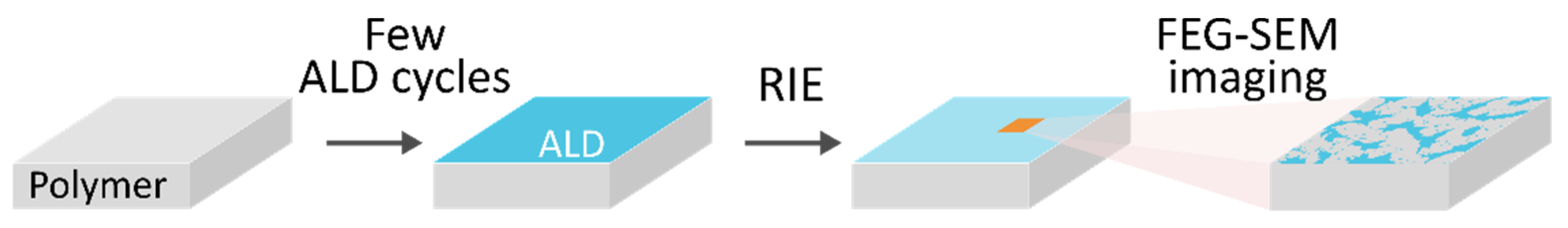
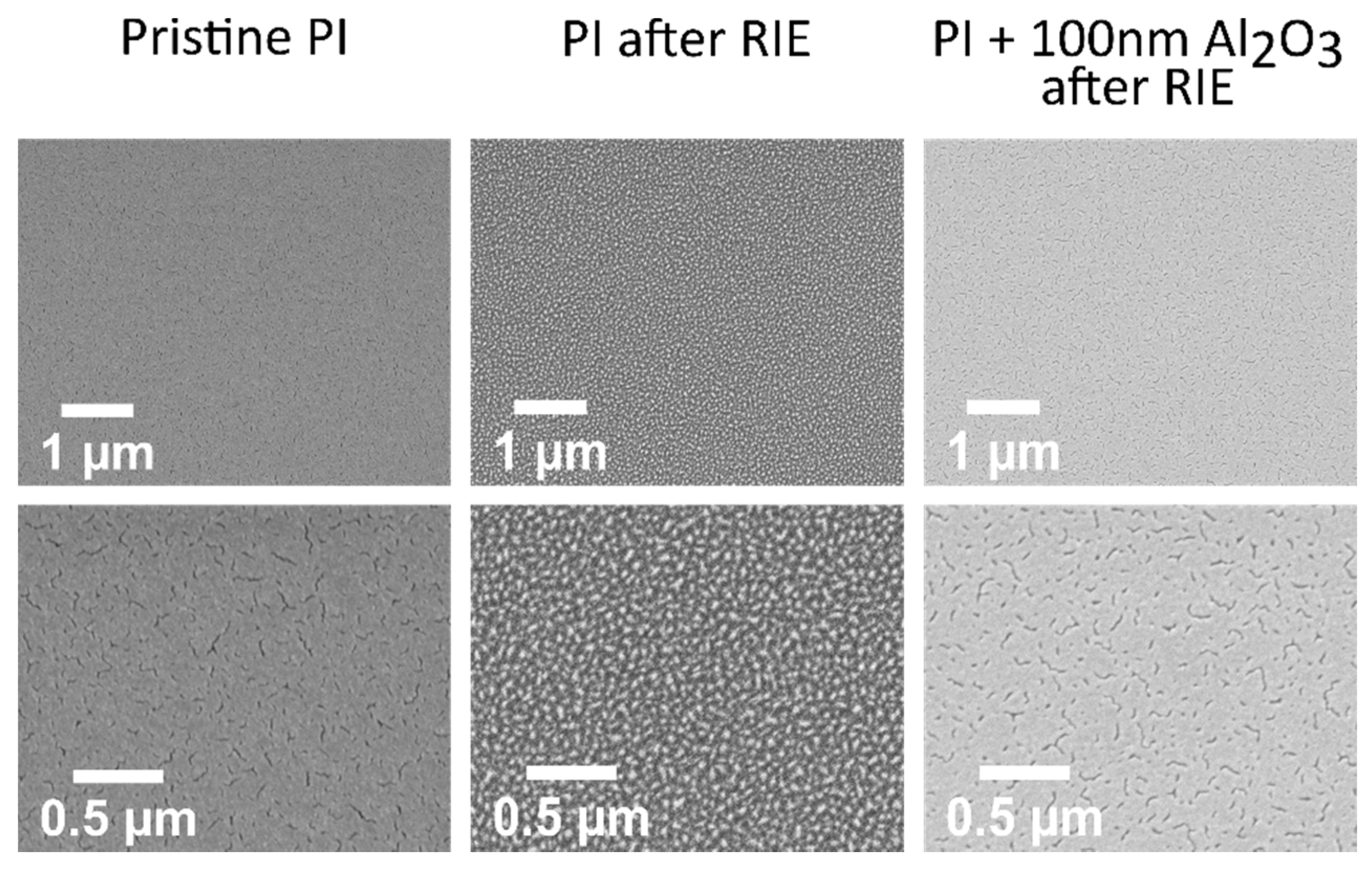
2.2.1. Sample Preparation
2.2.2. Characterization
3. Results and Discussion
3.1. Introduction
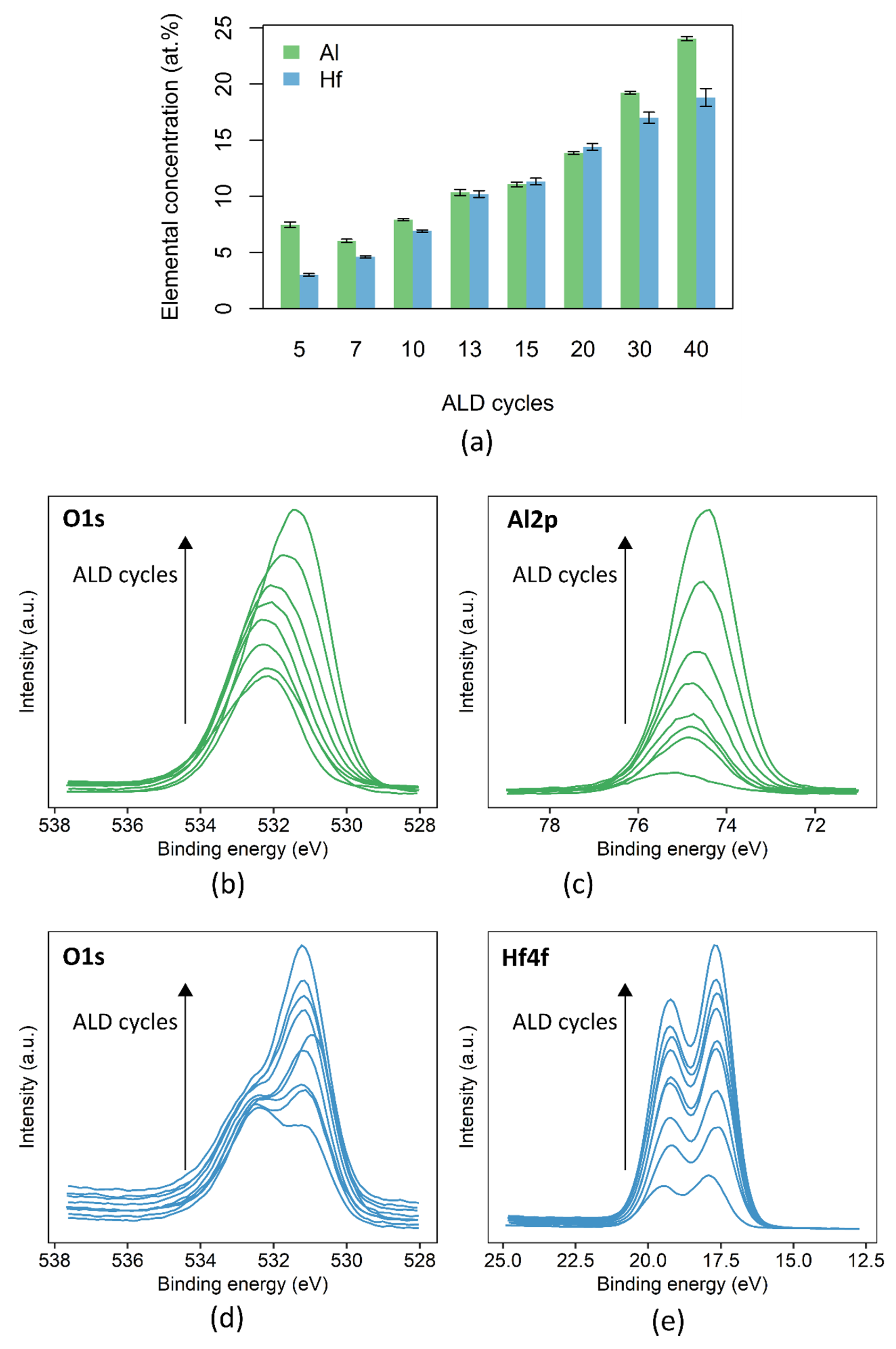
3.2. ALD Nucleation Study of Al2O3 and HfO2 on Polyimide
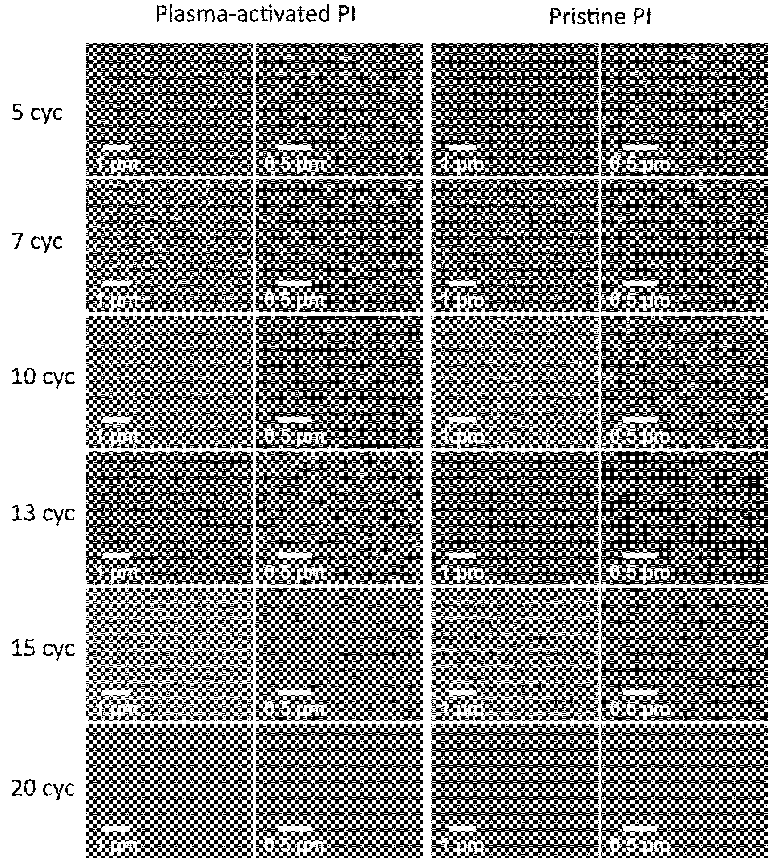
3.3. Influence of Plasma Activation on the ALD Nucleation
4. Conclusions
Supplementary Materials
Author Contributions
Funding
Institutional Review Board Statement
Informed Consent Statement
Data Availability Statement
Conflicts of Interest
References
- Leskelä, M.; Niinistö, J.; Ritala, M. 4.05—Atomic Layer Deposition. In Comprehensive Materials Processing; Hashmi, S., Batalha, G.F., van Tyne, C.J., Yilbas, B., Eds.; Elsevier: Oxford, UK, 2014; pp. 101–123. [Google Scholar]
- Knoops, H.C.M.; Potts, S.E.; Bol, A.A.; Kessels, W.M.M. 27—Atomic Layer Deposition. In Handbook of Crystal Growth, 2nd ed.; Kuech, T.F., Ed.; North-Holland: Boston, MA, USA, 2015; pp. 1101–1134. [Google Scholar]
- Atomic Limits. Available online: https://www.atomiclimits.com/alddatabase/ (accessed on 1 October 2021).
- Pakkala, A.; Putkonen, M. Chapter 8—Atomic Layer Deposition. In Handbook of Deposition Technologies for Films and Coatings, 3rd ed.; Martin, P.M., Ed.; William Andrew Publishing: Boston, MA, USA, 2010; pp. 364–391. [Google Scholar]
- Pessa, M.; Mäkelä, R.; Suntola, T. Characterization of surface exchange reactions used to grow compound films. Appl. Phys. Lett. 1981, 38, 131–132. [Google Scholar] [CrossRef]
- Tanninen, V.P.; Oikkonen, M.; Tuomi, T.O. X-ray diffraction study of thin electroluminescent ZnS films grown by atomic layer epitaxy. Phys. Status Solidi (A) 1981, 67, 573–583. [Google Scholar] [CrossRef]
- Busse, W.; Gumlich, H.E.; Törnqvist, R.O.; Tanninen, V.P. Zero-phonon lines in electroluminescence and photoluminescence of ZnS:Mn thin films grown by atomic layer epitaxy. Phys. Status Solidi (A) 1983, 76, 553–558. [Google Scholar] [CrossRef]
- Napari, M.; Malm, J.; Lehto, R.; Julin, J.; Arstila, K.; Sajavaara, T.; Lahtinen, M. Nucleation and growth of ZnO on PMMA by low-temperature atomic layer deposition. J. Vac. Sci. Technol. A 2014, 33, 01A128. [Google Scholar] [CrossRef] [Green Version]
- Kemell, M.; Färm, E.; Ritala, M.; Leskelä, M. Surface modification of thermoplastics by atomic layer deposition of Al2O3 and TiO2 thin films. Eur. Polym. J. 2008, 44, 3564–3570. [Google Scholar] [CrossRef]
- Hyde, G.K.; Scarel, G.; Spagnola, J.C.; Peng, Q.; Lee, K.; Gong, B.; Roberts, K.G.; Roth, K.M.; Hanson, C.A.; Devine, C.K.; et al. Atomic Layer Deposition and Abrupt Wetting Transitions on Nonwoven Polypropylene and Woven Cotton Fabrics. Langmuir 2010, 26, 2550–2558. [Google Scholar] [CrossRef]
- Pessoa, R.S.; Santos, V.P.d.; Cardoso, S.B.; Doria, A.C.O.C.; Figueira, F.R.; Rodrigues, B.V.M.; Testoni, G.E.; Fraga, M.A.; Marciano, F.R.; Lobo, A.O.; et al. TiO2 coatings via atomic layer deposition on polyurethane and polydimethylsiloxane substrates: Properties and effects on C. albicans growth and inactivation process. Appl. Surf. Sci. 2017, 422, 73–84. [Google Scholar] [CrossRef]
- Lindholm, N.F.; Zhang, J.; Minton, T.K.; O’Patchen, J.; George, S.M.; Groner, M.D. Protection of polymers from the space environment by atomic layer deposition. In AIP Conference Proceedings; American Institute of Physics: College Park, MD, USA, 2009; pp. 407–418. [Google Scholar]
- Cooper, R.; Upadhyaya, H.P.; Minton, T.K.; Berman, M.R.; Du, X.; George, S.M. Protection of polymer from atomic-oxygen erosion using Al2O3 atomic layer deposition coatings. Thin Solid Film. 2008, 516, 4036–4039. [Google Scholar] [CrossRef]
- Weber, M.; Julbe, A.; Kim, S.S.; Bechelany, M. Atomic layer deposition (ALD) on inorganic or polymeric membranes. J. Appl. Phys. 2019, 126, 041101. [Google Scholar] [CrossRef]
- Sweet, W.J.; I, I.I.; Oldham, C.J.; Parsons, G.N. Conductivity and touch-sensor application for atomic layer deposition ZnO and Al:ZnO on nylon nonwoven fiber mats. J. Vac. Sci. Technol. A Vac. Surf. Film. 2015, 33, 01A117. [Google Scholar] [CrossRef]
- Sun, C.; Zhang, J.; Zhang, Y.; Zhao, F.; Xie, J.; Liu, Z.; Zhuang, J.; Zhang, N.; Ren, W.; Ye, Z.-G. Design and fabrication of flexible strain sensor based on ZnO-decorated PVDF via atomic layer deposition. Appl. Surf. Sci. 2021, 562, 150126. [Google Scholar] [CrossRef]
- Ras, R.H.A.; Kemell, M.; de Wit, J.; Ritala, M.; ten Brinke, G.; Leskelä, M.; Ikkala, O. Hollow Inorganic Nanospheres and Nanotubes with Tunable Wall Thicknesses by Atomic Layer Deposition on Self-Assembled Polymeric Templates. Adv. Mater. 2007, 19, 102–106. [Google Scholar] [CrossRef] [Green Version]
- Oldham, C.J.; Gong, B.; Spagnola, J.C.; Jur, J.S.; Senecal, K.J.; Godfrey, T.A.; Parsons, G.N. Atomic layer deposition on polymers: Applications to physical encapsulation of electrospun nylon nanofibers. ECS Trans. 2010, 33, 279–290. [Google Scholar] [CrossRef]
- Lee, J.Y.; Shin, C.M.; Heo, J.H.; Kim, C.R.; Park, J.H.; Lee, T.M.; Ryu, H.; Son, C.S.; Shin, B.C.; Lee, W.J. Effects of O2 plasma pre-treatment on ZnO thin films grown on polyethersulfone substrates at various deposition temperatures by atomic layer deposition. Curr. Appl. Phys. 2010, 10, S290–S293. [Google Scholar] [CrossRef]
- Heo, J.H.; Ryu, H.; Lee, W.J. Effect of O2 plasma pretreatment on structural and optical properties of ZnO films on PES substrate by atomic layer deposition. J. Ind. Eng. Chem. 2013, 19, 1638–1641. [Google Scholar] [CrossRef]
- Choi, S.W.; Park, J.Y.; Lee, C.; Lee, J.G.; Kim, S.S. Synthesis of highly crystalline hollow TiO2 fibers using atomic layer deposition on polymer templates. J. Am. Ceram. Soc. 2011, 94, 1974–1977. [Google Scholar] [CrossRef]
- Vähä-Nissi, M.; Pitkänen, M.; Salo, E.; Kenttä, E.; Tanskanen, A.; Sajavaara, T.; Putkonen, M.; Sievänen, J.; Sneck, A.; Rättö, M.; et al. Antibacterial and barrier properties of oriented polymer films with ZnO thin films applied with atomic layer deposition at low temperatures. Thin Solid Film. 2014, 562, 331–337. [Google Scholar] [CrossRef]
- Matsumae, T.; Dushatinski, T.; Abdel-Fattah, T.M.; Suga, T.; Zhang, K.; Chen, X.; Baumgart, H. Room Temperate Bonding of Al2O3 Layers by Atomic Layer Deposition on Polyimide Substrates. ECS Trans. 2015, 69, 99–105. [Google Scholar] [CrossRef]
- Kääriäinen, T.O.; Maydannik, P.; Cameron, D.C.; Lahtinen, K.; Johansson, P.; Kuusipalo, J. Atomic layer deposition on polymer based flexible packaging materials: Growth characteristics and diffusion barrier properties. Thin Solid Film. 2011, 519, 3146–3154. [Google Scholar] [CrossRef]
- Groner, M.D.; George, S.M.; McLean, R.S.; Carcia, P.F. Gas diffusion barriers on polymers using Al2O3 atomic layer deposition. Appl. Phys. Lett. 2006, 88, 1–3. [Google Scholar] [CrossRef]
- Ferrari, S.; Perissinotti, F.; Peron, E.; Fumagalli, L.; Natali, D.; Sampietro, M. Atomic layer deposited Al2O3 as a capping layer for polymer based transistors. Org. Electron. 2007, 8, 407–414. [Google Scholar] [CrossRef]
- Ferguson, J.D.; Weimer, A.W.; George, S.M. Atomic Layer Deposition of Al2O3 Films on Polyethylene Particles. Chem. Mater. 2004, 16, 5602–5609. [Google Scholar] [CrossRef]
- Chawla, V.; Ruoho, M.; Weber, M.; Chaaya, A.A.; Taylor, A.A.; Charmette, C.; Miele, P.; Bechelany, M.; Michler, J.; Utke, I. Fracture mechanics and oxygen gas barrier properties of Al2O3/ZnO nanolaminates on PET deposited by atomic layer deposition. Nanomaterials 2019, 9, 88. [Google Scholar] [CrossRef] [Green Version]
- Langereis, E.; Creatore, M.; Heil, S.B.S.; van de Sanden, M.C.M.; Kessels, W.M.M. Plasma-assisted atomic layer deposition of Al2O3 moisture permeation barriers on polymers. Appl. Phys. Lett. 2006, 89, 081915. [Google Scholar] [CrossRef]
- Carcia, P.F.; McLean, R.S.; Walls, D.J.; Reilly, M.H.; Wyre, J.P. Effect of early stage growth on moisture permeation of thin-film Al2O3 grown by atomic layer deposition on polymers. J. Vac. Sci. Technol. A Vac. Surf. Film. 2013, 31, 061507. [Google Scholar] [CrossRef]
- Carcia, P.F.; McLean, R.S.; Reilly, M.H.; Groner, M.D.; George, S.M. Ca test of Al2O3 gas diffusion barriers grown by atomic layer deposition on polymers. Appl. Phys. Lett. 2006, 89, 031915. [Google Scholar] [CrossRef] [Green Version]
- Carcia, P.F.; McLean, R.S.; Reilly, M.H. Permeation measurements and modeling of highly defective Al2O3 thin films grown by atomic layer deposition on polymers. Appl. Phys. Lett. 2010, 97, 221901. [Google Scholar] [CrossRef]
- Carcia, P.F.; McLean, R.S.; Li, Z.G.; Reilly, M.H.; Marshall, W.J. Permeability and corrosion in ZrO2/Al2O3 nanolaminate and Al2O3 thin films grown by atomic layer deposition on polymers. J. Vac. Sci. Technol. A Vac. Surf. Film. 2012, 30, 041515. [Google Scholar] [CrossRef]
- Hoyas, A.M.; Schuhmacher, J.; Shamiryan, D.; Waeterloos, J.; Besling, W.; Celis, J.P.; Maex, K. Growth and characterization of atomic layer deposited WC0.7N0.3 on polymer films. J. Appl. Phys. 2004, 95, 381–388. [Google Scholar] [CrossRef]
- Elam, J.W.; Wilson, C.A.; Schuisky, M.; Sechrist, Z.A.; George, S.M. Improved nucleation of TiN atomic layer deposition films on SiLK low-k polymer dielectric using an Al2O3 atomic layer deposition adhesion layer. J. Vac. Sci. Technol. B Microelectron. Nanometer Struct. 2003, 21, 1099–1107. [Google Scholar] [CrossRef]
- Song, E.; Li, R.; Jin, X.; Du, H.; Huang, Y.; Zhang, J.; Xia, Y.; Fang, H.; Lee, Y.K.; Yu, K.J.; et al. Ultrathin Trilayer Assemblies as Long-Lived Barriers against Water and Ion Penetration in Flexible Bioelectronic Systems. ACS Nano 2018, 12, 10317–10326. [Google Scholar] [CrossRef]
- Jeong, J.; Laiwalla, F.; Lee, J.; Ritasalo, R.; Pudas, M.; Larson, L.; Leung, V.; Nurmikko, A. Conformal Hermetic Sealing of Wireless Microelectronic Implantable Chiplets by Multilayered Atomic Layer Deposition (ALD). Adv. Funct. Mater. 2019, 29, 1806440. [Google Scholar] [CrossRef]
- Peron, M.; Cogo, S.; Bjelland, M.; Afif, A.B.; Dadlani, A.; Greggio, E.; Berto, F.; Torgersen, J. On the evaluation of ALD TiO2, ZrO2 and HfO2 coatings on corrosion and cytotoxicity performances. J. Magnes. Alloy. 2021, 9, 1806–1819. [Google Scholar] [CrossRef]
- Xie, X.; Rieth, L.; Merugu, S.; Tathireddy, P.; Solzbacher, F. Plasma-assisted atomic layer deposition of Al2O3 and parylene C bi-layer encapsulation for chronic implantable electronics. Appl. Phys. Lett. 2012, 101, 093702. [Google Scholar] [CrossRef] [Green Version]
- Xie, X.; Rieth, L.; Caldwell, R.; Diwekar, M.; Tathireddy, P.; Sharma, R.; Solzbacher, F. Long-Term Bilayer Encapsulation Performance of Atomic Layer Deposited Al2O3 and Parylene C for Biomedical Implantable Devices. IEEE Trans. Biomed. Eng. 2013, 60, 2943–2951. [Google Scholar] [PubMed]
- Minnikanti, S.; Diao, G.; Pancrazio, J.J.; Xie, X.; Rieth, L.; Solzbacher, F.; Peixoto, N. Lifetime assessment of atomic-layer-deposited Al2O3–Parylene C bilayer coating for neural interfaces using accelerated age testing and electrochemical characterization. Acta Biomater. 2014, 10, 960–967. [Google Scholar] [CrossRef]
- Xie, X.; Rieth, L.; Williams, L.; Negi, S.; Bhandari, R.; Caldwell, R.; Sharma, R.; Tathireddy, P.; Solzbacher, F. Long-term reliability of Al2O3 and Parylene C bilayer encapsulated Utah electrode array based neural interfaces for chronic implantation. J. Neural Eng. 2014, 11, 026016. [Google Scholar] [CrossRef] [PubMed] [Green Version]
- Xie, X.; Rieth, L.W.; Sharma, R.; Negi, S.; Bhandari, R.; Caldwell, R.; Tathireddy, P.; Solzbacher, F. Atomic Layer Deposited Al2O3 and Parylene C Bi-layer Encapsulation for Utah Electrode Array Based Neural Interfaces. MRS Online Proc. Libr. 2014, 1621, 259–265. [Google Scholar] [CrossRef]
- Caldwell, R.; Rieth, L.; Xie, X.; Sharma, R.; Solzbacher, F.; Tathireddy, P. Failure mode analysis of Al2O2-parylene c bilayer encapsulation for implantable devices and application to penetrating neural arrays. In Proceedings of the 2015 Transducers—2015 18th International Conference on Solid-State Sensors, Actuators and Microsystems (TRANSDUCERS), Anchorage, AK, USA, 21–25 June 2015; pp. 1747–1750. [Google Scholar]
- Xie, X.; Rieth, L.; Caldwell, R.; Negi, S.; Bhandari, R.; Sharma, R.; Tathireddy, P.; Solzbacher, F. Effect of bias voltage and temperature on lifetime of wireless neural interfaces with Al2O3 and parylene bilayer encapsulation. Biomed. Microdevices 2015, 17, 1. [Google Scholar] [CrossRef]
- Caldwell, R.; Mandal, H.; Sharma, R.; Solzbacher, F.; Tathireddy, P.; Rieth, L. Analysis of Al2O3—parylene C bilayer coatings and impact of microelectrode topography on long term stability of implantable neural arrays. J. Neural Eng. 2017, 14, 046011. [Google Scholar] [CrossRef]
- Guo, H.C.; Ye, E.; Li, Z.; Han, M.-Y.; Loh, X.J. Recent progress of atomic layer deposition on polymeric materials. Mater. Sci. Eng. C 2017, 70, 1182–1191. [Google Scholar] [CrossRef]
- Parsons, G.N.; Atanasov, S.E.; Dandley, E.C.; Devine, C.K.; Gong, B.; Jur, J.S.; Lee, K.; Oldham, C.J.; Peng, Q.; Spagnola, J.C.; et al. Mechanisms and reactions during atomic layer deposition on polymers. Coord. Chem. Rev. 2013, 257, 3323–3331. [Google Scholar] [CrossRef]
- Losego, M.D.; Peng, Q. Atomic layer deposition and vapor phase infiltration. In Surface Modification of Polymers: Methods and Applications; Wiley: Hoboken, NJ, USA, 2019; pp. 135–159. [Google Scholar]
- Waldman, R.Z.; Mandia, D.J.; Yanguas-Gil, A.; Martinson, A.B.F.; Elam, J.W.; Darling, S.B. The chemical physics of sequential infiltration synthesis—A thermodynamic and kinetic perspective. J. Chem. Phys. 2019, 151, 190901. [Google Scholar] [CrossRef]
- Ashurbekova, K.; Ashurbekova, K.; Botta, G.; Yurkevich, O.; Knez, M. Vapor phase processing: A novel approach for fabricating functional hybrid materials. Nanotechnology 2020, 31, 342001. [Google Scholar] [CrossRef]
- Brandt, E.S.; Grace, J.M. Initiation of atomic layer deposition of metal oxides on polymer substrates by water plasma pretreatment. J. Vac. Sci. Technol. A 2011, 30, 01A137. [Google Scholar] [CrossRef]
- Lee, G.B.; Son, K.S.; Park, S.W.; Shim, J.H.; Choi, B.-H. Low-temperature atomic layer deposition of Al2O3 on blown polyethylene films with plasma-treated surfaces. J. Vac. Sci. Technol. A 2012, 31, 01A129. [Google Scholar]
- Park, S.W.; Bae, K.; Kim, J.W.; Lee, G.B.; Choi, B.-H.; Lee, M.H.; Shim, J.H. Chemical Protection of Polycarbonate Surfaces by Atomic Layer Deposition of Alumina with Oxygen Plasma Pretreatment. Adv. Mater. Interfaces 2016, 3, 1600340. [Google Scholar] [CrossRef]
- Song, S.H.; Lee, M.Y.; Lee, G.B.; Choi, B.-H. Characterization of Al2O3 and ZnO multilayer thin films deposited by low temperature thermal atomic layer deposition on transparent polyimide. J. Vac. Sci. Technol. A 2016, 35, 01B110. [Google Scholar] [CrossRef]
- Krumpolec, R.; Cameron, D.C.; Homola, T.; Černák, M. Surface chemistry and initial growth of Al2O3 on plasma modified PTFE studied by ALD. Surf. Interfaces 2017, 6, 223–228. [Google Scholar] [CrossRef]
- Frank, M.M.; Chabal, Y.J.; Wilk, G.D. Nucleation and interface formation mechanisms in atomic layer deposition of gate oxides. Appl. Phys. Lett. 2003, 82, 4758–4760. [Google Scholar] [CrossRef]
- Wilson, C.A.; Grubbs, R.K.; George, S.M. Nucleation and Growth during Al2O3 Atomic Layer Deposition on Polymers. Chem. Mater. 2005, 17, 5625–5634. [Google Scholar] [CrossRef]
- Kirsch, P.D.; Quevedo-Lopez, M.A.; Li, H.J.; Senzaki, Y.; Peterson, J.J.; Song, S.C.; Krishnan, S.A.; Moumen, N.; Barnett, J.; Bersuker, G.; et al. Nucleation and growth study of atomic layer deposited HfO2 gate dielectrics resulting in improved scaling and electron mobility. J. Appl. Phys. 2006, 99, 023508. [Google Scholar] [CrossRef]
- Elam, J.W.; Zinovev, A.V.; Pellin, M.J.; Comstock, D.J.; Hersam, M.C. Nucleation and growth of noble metals on oxide surfaces using atomic layer deposition. ECS Trans. 2007, 3, 271–278. [Google Scholar] [CrossRef]
- Lee, J.S.; Kaufman-Osborn, T.; Melitz, W.; Lee, S.; Delabie, A.; Sioncke, S.; Caymax, M.; Pourtois, G.; Kummel, A.C. Atomic imaging of nucleation of trimethylaluminum on clean and H2O functionalized Ge(100) surfaces. J. Chem. Phys. 2011, 135, 054705. [Google Scholar] [CrossRef]
- Lei, Y.; Lu, J.; Zhao, H.; Liu, B.; Low, K.-B.; Wu, T.; Libera, J.A.; Greeley, J.P.; Chupas, P.J.; Miller, J.T.; et al. Resolving Precursor Deligation, Surface Species Evolution, and Nanoparticle Nucleation during Palladium Atomic Layer Deposition. J. Phys. Chem. C 2013, 117, 11141–11148. [Google Scholar] [CrossRef]
- Alivio, T.E.G.; de Jesus, L.R.; Dennis, R.V.; Jia, Y.; Jaye, C.; Fischer, D.A.; Singisetti, U.; Banerjee, S. Atomic Layer Deposition of Hafnium(IV) Oxide on Graphene Oxide: Probing Interfacial Chemistry and Nucleation by using X-ray Absorption and Photoelectron Spectroscopies. ChemPhysChem 2015, 16, 2842–2848. [Google Scholar] [CrossRef]
- Walter, T.N.; Lee, S.; Zhang, X.; Chubarov, M.; Redwing, J.M.; Jackson, T.N.; Mohney, S.E. Atomic layer deposition of ZnO on MoS2 and WSe2. Appl. Surf. Sci. 2019, 480, 43–51. [Google Scholar] [CrossRef]
- Gakis, G.P.; Vahlas, C.; Vergnes, H.; Dourdain, S.; Tison, Y.; Martinez, H.; Bour, J.; Ruch, D.; Boudouvis, A.G.; Caussat, B.; et al. Investigation of the initial deposition steps and the interfacial layer of Atomic Layer Deposited (ALD) Al2O3 on Si. Appl. Surf. Sci. 2019, 492, 245–254. [Google Scholar] [CrossRef]
- Astaneh, S.H.; Jursich, G.; Sukotjo, C.; Takoudis, C.G. Surface and subsurface film growth of titanium dioxide on polydimethylsiloxane by atomic layer deposition. Appl. Surf. Sci. 2019, 493, 779–786. [Google Scholar] [CrossRef]
- Su, D.-Y.; Kuo, Y.-H.; Tseng, M.-H.; Tsai, F.-Y. Effects of surface pretreatment and deposition conditions on the gas permeation properties and flexibility of Al2O3 films on polymer substrates by atomic layer deposition. J. Coat. Technol. Res. 2019, 16, 1751–1756. [Google Scholar] [CrossRef]
- Reif, J.; Knaut, M.; Killge, S.; Albert, M.; Bartha, J.W. In vacuo investigations on the nucleation of TaCN by plasma enhanced atomic layer deposition. Microelectron. Eng. 2019, 211, 13–17. [Google Scholar] [CrossRef]
- Zhu, H.; Addou, R.; Wang, Q.; Nie, Y.; Cho, K.; Kim, M.J.; Wallace, R.M. Surface and interfacial study of atomic layer deposited Al2O3 on MoTe2 and WTe2. Nanotechnology 2020, 31, 055704. [Google Scholar] [CrossRef] [PubMed]
- Puurunen, R.L.; Vandervorst, W.; Besling, W.F.A.; Richard, O.; Bender, H.; Conard, T.; Zhao, C.; Delabie, A.; Caymax, M.; de Gendt, S.; et al. Island growth in the atomic layer deposition of zirconium oxide and aluminum oxide on hydrogen-terminated silicon: Growth mode modeling and transmission electron microscopy. J. Appl. Phys. 2004, 96, 4878–4889. [Google Scholar] [CrossRef]
- Thian, D.; Yemane, Y.T.; Xu, S.; Prinz, F.B. Methodology for Studying Surface Chemistry and Evolution during the Nucleation Phase of Atomic Layer Deposition Using Scanning Tunneling Microscopy. J. Phys. Chem. C 2017, 121, 27379–27388. [Google Scholar] [CrossRef]
- Kim, D.-H.; Ghaffari, R.; Lu, N.; Rogers, J.A. Flexible and Stretchable Electronics for Biointegrated Devices. Annu. Rev. Biomed. Eng. 2012, 14, 113–128. [Google Scholar] [CrossRef] [Green Version]
- Poppendieck, W.; Sossalla, A.; Krob, M.-O.; Welsch, C.; Nguyen, T.A.K.; Gong, W.; DiGiovanna, J.; Micera, S.; Merfeld, D.M.; Hoffmann, K.-P. Development, manufacturing and application of double-sided flexible implantable microelectrodes. Biomed. Microdevices 2014, 16, 837–850. [Google Scholar] [CrossRef]
- Lee, H.C.; Ejserholm, F.; Gaire, J.; Currlin, S.; Schouenborg, J.; Wallman, L.; Bengtsson, M.; Park, K.; Otto, K.J. Histological evaluation of flexible neural implants; flexibility limit for reducing the tissue response? J. Neural Eng. 2017, 14, 036026. [Google Scholar] [CrossRef] [Green Version]
- Kassanos, P.; Anastasova, S.; Chen, C.M.; Yang, G.-Z. Sensor Embodiment and Flexible Electronics. In Implantable Sensors and Systems: From Theory to Practice; Yang, G.-Z., Ed.; Springer International Publishing: Cham, Switzerland, 2018; pp. 197–279. [Google Scholar]
- Verplancke, R.; Cauwe, M.; Schaubroeck, D.; Cuypers, D.; Vandecasteele, B.; Mader, L.; Vanhaverbeke, C.; Ballini, M.; O’Callaghan, J.; Goikoetxea, E.; et al. Development of an active high-density transverse intrafascicular micro-electrode probe. J. Micromech. Microeng. 2019, 30, 015010. [Google Scholar] [CrossRef]
- Vandekerckhove, B.; Missinne, J.; Vonck, K.; Bauwens, P.; Verplancke, R.; Boon, P.; Raedt, R.; Vanfleteren, J. Technological Challenges in the Development of Optogenetic Closed-Loop Therapy Approaches in Epilepsy and Related Network Disorders of the Brain. Micromachines 2021, 12, 38. [Google Scholar] [CrossRef]
- Li, C.; Cauwe, M.; Mader, L.; Schaubroeck, D.; de Beeck, M.O. Accelerated Hermeticity Testing of Biocompatible Moisture Barriers Used for the Encapsulation of Implantable Medical Devices. Coatings 2020, 10, 19. [Google Scholar] [CrossRef] [Green Version]
- Li, C.; Cauwe, M.; Yang, Y.; Schaubroeck, D.; Mader, L.; de Beeck, M.O. Ultra-Long-Term Reliable Encapsulation Using an Atomic Layer Deposited HfO2/Al2O3/HfO2 Triple-Interlayer for Biomedical Implants. Coatings 2019, 9, 579. [Google Scholar] [CrossRef] [Green Version]
- Fahim, M.; Bijwe, J.; Nalwa, H.S. Chapter 8—Polyimides for Microelectronics and Tribology Applications. In Supramolecular Photosensitive and Electroactive Materials; Nalwa, H.S., Ed.; Academic Press: San Diego, CA, USA, 2001; pp. 643–726. [Google Scholar]
- Liaw, D.J.; Wang, K.L.; Huang, Y.C.; Lee, K.R.; Lai, J.Y.; Ha, C.S. Advanced polyimide materials: Syntheses, physical properties and applications. Prog. Polym. Sci. 2012, 37, 907–974. [Google Scholar] [CrossRef]
- Qin, Y.; Howlader, M.M.R.; Deen, M.J.; Haddara, Y.M.; Selvaganapathy, P.R. Polymer integration for packaging of implantable sensors. Sens. Actuators B Chem. 2014, 202, 758–778. [Google Scholar] [CrossRef]
- Ghosh, M.K.; Mittal, K.L. Polyimides: Fundamentals and Applications; CRC Press: Boca Raton, FL, USA, 2018. [Google Scholar]
- Bryant, R.G. Polyimides. In Ullmann’s Encyclopedia of Industrial Chemistry. 2014. Available online: https://en.wikipedia.org/wiki/Ullmann’s_Encyclopedia_of_Industrial_Chemistry (accessed on 1 October 2021).
- Patrick, E.; Sankar, V.; Rowe, W.; Sheng-Feng, Y.; Sanchez, J.C.; Toshikazu, N. Flexible polymer substrate and tungsten microelectrode array for an implantable neural recording system. In Proceedings of the 2008 30th Annual International Conference of the IEEE Engineering in Medicine and Biology Society, Vancouver, BC, Canada, 21–24 August 2008; pp. 3158–3161. [Google Scholar]
- Winkin, N.; Mokwa, W. Flexible multi-electrode array with integrated bendable CMOS-chip for implantable systems. In Proceedings of the 2012 Annual International Conference of the IEEE Engineering in Medicine and Biology Society, San Diego, CA, USA, 28 August–1 September 2012; pp. 3882–3885. [Google Scholar]
- Kirsten, S.; Schubert, M.; Braunschweig, M.; Woldt, G.; Voitsekhivska, T.; Wolter, K.J. Biocompatible packaging for implantable miniaturized pressure sensor device used for stent grafts: Concept and choice of materials. In Proceedings of the Proceedings of the 16th Electronics Packaging Technology Conference, EPTC 2014, Singapore, 3–5 December 2014; pp. 719–724. [Google Scholar]
- Schubert, M.; Kirsten, S.; Voitsekhivska, T.; Bock, K. Characterization of polymeric encapsulation for implantable microsystems applying dynamic fluidic and electrical load. In Proceedings of the Proceedings of the International Spring Seminar on Electronics Technology, Eger, Hungary, 6–10 May 2015; pp. 129–133. [Google Scholar]
- Tolstosheeva, E.; Biefeld, V.; Lang, W. Accelerated soak performance of BPDA-PPD polyimide for implantable MEAs. Procedia Eng. 2015, 120, 36–40. [Google Scholar] [CrossRef] [Green Version]
- Lee, J.H.; Kim, H.; Kim, J.H.; Lee, S.-H. Soft implantable microelectrodes for future medicine: Prosthetics, neural signal recording and neuromodulation. Lab Chip 2016, 16, 959–976. [Google Scholar] [CrossRef]
- Beeck, M.O.d.; Verplancke, R.; Schaubroeck, D.; Cuypers, D.; Cauwe, M.; Vandecasteele, B.; Callaghan, J.O.; Braeken, D.; Andrei, A.; Firrincieli, A.; et al. Ultra-thin biocompatible implantable chip for bidirectional communication with peripheral nerves. In Proceedings of the 2017 IEEE Biomedical Circuits and Systems Conference (BioCAS), Torino, Italy, 19–21 October 2017; pp. 1–4. [Google Scholar]
- Bleck, L.; Steins, H.; von Metzen, R. Interface Adhesion in Implantable Chip-in-Foil Systems. In Proceedings of the Proceedings of the Annual International Conference of the IEEE Engineering in Medicine and Biology Society, EMBS, Dubai, United Arab Emirates, 12–15 November 2018; pp. 2981–2984. [Google Scholar]
- Li, C. Long-Term Miniaturized Flexible Hermetic Encapsulation for Implantable Medical Devices Using Polymers and Atomic Layer Deposited Ceramics; Department of Electronics and Information Systems, Ghent University: Ghent, Belgium, 2020. [Google Scholar]
- Steckl, A.J.; Balakrishnan, S.; Jin, H.S.; Corelli, J.C. Micromachining of polyimide films with focused ion beams. Microelectron. Eng. 1986, 5, 461–462. [Google Scholar] [CrossRef]
- al Hashimi, H.; Chaalal, O. Flexible temperature sensor fabrication using photolithography technique. Therm. Sci. Eng. Prog. 2021, 22, 100857. [Google Scholar] [CrossRef]
- Rajawat, S.; Hübner, M.; Kempen, L.; Lang, W. Flexible passive LC resonator for wireless measurement during curing of thermosets. J. Phys. Conf. Ser. 2021, 1837, 012001. [Google Scholar]
- Kuliasha, C.A.; Judy, J.W. The Materials Science Foundation Supporting the Microfabrication of Reliable Polyimide–Metal Neuroelectronic Interfaces. Adv. Mater. Technol. 2021, 6, 2100149. [Google Scholar] [CrossRef]
- Ahn, S.-H.; Jeong, J.; Kim, S.J. Emerging Encapsulation Technologies for Long-Term Reliability of Microfabricated Implantable Devices. Micromachines 2019, 10, 508. [Google Scholar] [CrossRef] [Green Version]
- Forssell, M.; Ong, X.C.; Fedder, G.K. Multilayer ALD ceramic films for enhancement of parylene barrier properties in compliant neural probes with bonded chips. In Proceedings of the 2018 Solid-State Sensors, Actuators and Microsystems Workshop, Hilton Head Island, SC, USA, 3–7 June 2018; pp. 272–275. [Google Scholar]
- Astoreca, L.; Cools, P.; Schaubroeck, D.; Asadian, M.; Aliakbarshirazi, S.; Declercq, H.; de Beeck, M.O.; Morent, R.; de Smet, H.; de Geyter, N. Non-thermal plasma activation of BPDA-PPD polyimide for improved cell-material interaction. Polymer 2020, 205, 122831. [Google Scholar] [CrossRef]
- Buder, U.; von Klitzing, J.P.; Obermeier, E. Reactive ion etching for bulk structuring of polyimide. Sens. Actuators A Phys. 2006, 132, 393–399. [Google Scholar] [CrossRef]
- Zhang, Y.; Guerra-Nuñez, C.; Utke, I.; Michler, J.; Rossell, M.D.; Erni, R. Understanding and Controlling Nucleation and Growth of TiO2 Deposited on Multiwalled Carbon Nanotubes by Atomic Layer Deposition. J. Phys. Chem. C 2015, 119, 3379–3387. [Google Scholar] [CrossRef]
- Schilirò, E.; Nigro, R.L.; Panasci, S.E.; Gelardi, F.M.; Agnello, S.; Yakimova, R.; Roccaforte, F.; Giannazzo, F. Aluminum oxide nucleation in the early stages of atomic layer deposition on epitaxial graphene. Carbon 2020, 169, 172–181. [Google Scholar] [CrossRef]
- Grigoras, K.; Sainiemi, L.; Tiilikainen, J.; Säynätjoki, A.; Airaksinen, V.M.; Franssila, S. Application of ultra-thin aluminum oxide etch mask made by atomic layer deposition technique. J. Phys. Conf. Ser. 2007, 61, 369–373. [Google Scholar] [CrossRef] [Green Version]
- Kim, H.G.; Lee, J.G.; Kim, S.S. Surface modification of polymeric substrates to enhance the barrier properties of an Al2O3 layer formed by PEALD process. Org. Electron. 2017, 50, 239–246. [Google Scholar] [CrossRef]


Publisher’s Note: MDPI stays neutral with regard to jurisdictional claims in published maps and institutional affiliations. |
© 2021 by the authors. Licensee MDPI, Basel, Switzerland. This article is an open access article distributed under the terms and conditions of the Creative Commons Attribution (CC BY) license (https://creativecommons.org/licenses/by/4.0/).
Share and Cite
Astoreca, L.; Schaubroeck, D.; Esbah Tabaei, P.S.; Ghobeira, R.; Op de Beeck, M.; Morent, R.; De Smet, H.; De Geyter, N. Investigating the Nucleation of AlOx and HfOx ALD on Polyimide: Influence of Plasma Activation. Coatings 2021, 11, 1352. https://doi.org/10.3390/coatings11111352
Astoreca L, Schaubroeck D, Esbah Tabaei PS, Ghobeira R, Op de Beeck M, Morent R, De Smet H, De Geyter N. Investigating the Nucleation of AlOx and HfOx ALD on Polyimide: Influence of Plasma Activation. Coatings. 2021; 11(11):1352. https://doi.org/10.3390/coatings11111352
Chicago/Turabian StyleAstoreca, Laura, David Schaubroeck, Parinaz Saadat Esbah Tabaei, Rouba Ghobeira, Maaike Op de Beeck, Rino Morent, Herbert De Smet, and Nathalie De Geyter. 2021. "Investigating the Nucleation of AlOx and HfOx ALD on Polyimide: Influence of Plasma Activation" Coatings 11, no. 11: 1352. https://doi.org/10.3390/coatings11111352
APA StyleAstoreca, L., Schaubroeck, D., Esbah Tabaei, P. S., Ghobeira, R., Op de Beeck, M., Morent, R., De Smet, H., & De Geyter, N. (2021). Investigating the Nucleation of AlOx and HfOx ALD on Polyimide: Influence of Plasma Activation. Coatings, 11(11), 1352. https://doi.org/10.3390/coatings11111352