Article

Integration of Fluorescent, NV-Rich Nanodiamond Particles with AFM Cantilevers by Focused Ion Beam for Hybrid Optical and Micromechanical Devices

1
Department of Metrology and Optoelectronics, Faculty of Electronics, Telecommunications and Informatics, Gdańsk University of Technology, G. Narutowcza 11/12, 80-233 Gdańsk, Poland
2
Department of Nanometrology, Faculty of Microsystem Electronics and Photonics, Wrocław University of Science and Technology, Janiszewskiego 11/17, 50-372 Wrocław, Poland
3
Department of Photonics, Institute of Physics, Jagiellonian University, St. Łojasiewicza 11, 30-348 Kraków, Poland
*
Author to whom correspondence should be addressed.
Coatings 2021, 11(11), 1332; https://doi.org/10.3390/coatings11111332
Submission received: 26 September 2021 / Revised: 18 October 2021 / Accepted: 27 October 2021 / Published: 29 October 2021
(This article belongs to the Special Issue Nanodiamond Hybrid Materials: Synthesis and Application)

Abstract

:
In this paper, a novel fabrication technology of atomic force microscopy (AFM) probes integrating cantilever tips with an NV-rich diamond particle is presented. Nanomanipulation techniques combined with the focused electron beam-induced deposition (FEBID) procedure were applied to position the NV-rich diamond particle on an AFM cantilever tip. Ultrasonic treatment of nanodiamond suspension was applied to reduce the size of diamond particles for proper geometry and symmetry. The fabricated AFM probes were tested utilizing measurements of the electrical resistance at highly oriented pyrolytic graphite (HOPG) and compared with a standard AFM cantilever performance. The results showed novel perspectives arising from combining the functionalities of a scanning AFM with optically detected magnetic resonance (ODMR). In particular, it offers enhanced magnetometric sensitivity and the nanometric resolution.

1. Introduction

Scanning probe magnetometry greatly benefits from utilising nitrogen-vacancy (NV) colour centres [1], which provide the systems with high spatial resolution that are extremely sensitive to magnetic fields and can operate across a broad range of temperatures [2]. Atomic force microscopy (AFM) technology is typically implemented to create nanosensors of magnetic fields based on diamond particles with NV centres. To provide maximum sensitivity of the sensors, it is important to keep the NV defects as close to the surface of the analysed material as possible, therefore the nanodiamonds are usually implanted on apexes of AFM tips. What remains challenging when using the NV centres as AFM scanning probes is the effective fabrication of the centres and providing an efficient collection of their optical signal. There have been many examples of scanning probe microscopy with diamond probes containing single NV centres for nanoscale magnetometry [3,4,5,6] with nanometer resolution. In these applications, single nanodiamonds with a nitrogen-vacancy (NV) centre coupled to an atomic force microscope (AFM), are helpful to quantitatively map the stray magnetic field, and for studies of nanomechanical properties of biological molecules, organelle, and living cells. The scanning NV magnetometry with single NV spins can also be used to detect weak perturbations of magnetic textures [7]. On the other hand, a different strategy was suggested in Ref. [4]. Rather than work with a single spin in a single NV, one can substantially increase magnetic sensitivity by working with high-density samples. In our paper, by attaching an NV-rich nano/micro-diamond to an AFM tip we combine the advantage of the latter route with the nanometric resolution offered by scanning microscopy.
The shape of the scanning tip plays an important role in the characterisation of the nanostructure. The effect of the tip shape on the recorded images has been studied since the beginning of scanning probe microscopy [8,9]. Typically, some areas of AFM images may contain tip-related artifacts, but in the worst scenarios, the images could be generated from a signal coming from the tip itself, and not the whole analysed surface [9,10]. The shape of the scanning tip influences not only the way the physical shape of the sample is recorded but also phenomena occurring between the scanning tip and the sample [11,12,13]. Typically, the AFM tip enabling atomic-scale resolution should have a small radius, but if the height or depth of the analysed object needs to be considered, the tip aspect ratio should also be taken into account [14,15]. The geometry of AFM cantilevers limits the latitude in positioning and orienting the nanodiamonds relative to the samples, and collecting the fluorescence emitted by the NV centres. One approach to make a diamond AFM tip is to cover the whole AFM tip with a diamond layer [16] or to make the AFM cantilever entirely out of the diamond [17]. An alternative approach is to manipulate the nanodiamond itself using optical tweezers or anti-Brownian electrokinetic traps. Kim et al. [18] developed specifically shaped microparticles coupled with an active platinum pad and a nanodiamond containing a NV centre, and utilised light-driven self-thermophoresis to induce their translational and rotational motions. Electron spin resonance (ESR) measurements carried out in a liquid environment in the presence of an external magnetic field have confirmed the potential of these microparticles for nanoscale magnetometry in biological systems.
Zhou et al. [19] described a simple procedure to efficiently produce scanning probes consisting of an integrated RF micro-antenna and a 3.5 μm-long diamond nanopillar containing a single NV centre, both fabricated directly onto an ultrapure diamond substrate. The probes may be glued directly to tipless silicon cantilevers for optical beam deflection-based AFM, as well as to pulled quartz rods, which are then attached to a tuning fork.
To increase the efficiency of photon collection from the colour centres, Choi et al. [20] gave up metal-coated Si cantilevers for transparent ones made of silicon nitride and reported a strong channelling effect while collecting the fluorescence of the NV centres from the apex towards the base of commercially available, pyramid-shaped diamond AFM tips. The enhanced photoluminescence collection was up to eight times higher compared to other directions.
In this study, a novel fabrication technology of an AFM cantilever tip integrating a NV-rich diamond particle is presented. Using ultrasonic treatment, the correct shape and size of the NV-rich diamond particle were obtained. Nanomanipulation techniques combined with the focussed electron beam-induced deposition (FEBID) procedure were applied to place the NV-rich diamond particle on an AFM cantilever tip. The fabricated probes were tested and used for optically detected magnetic resonance (ODMR).

2. Experimental Procedure

2.1. Preparation of NV-Rich Nanodiamond Particles

To obtain the correct shape and size of NV-rich nanodiamonds to be placed at the end of the AFM cantilever, we applied fragmentation of the particles by ultrasonic disintegration for various time durations [21]. 10 mg of commercially available, NV-rich nanodiamond particles (Adámas Nanotechnologies, Raleigh, NC, USA) with ~1 μm average particle size and up to 3 ppm of NV- centres were put into each of five identical polypropylene tubes that were subsequently filled with 10 mL of isopropyl alcohol (IPA). In that way, the same concentration of the NV-rich nanodiamond particles was obtained in every sample. The ultrasonic disintegration of the NV-rich nanodiamond particles was carried out using a Bandelin Sonopuls HD 2200 homogeniser (Bandelin, Berlin, Germany). No abrasive NV-rich diamond was chosen for the process, allowing the particles to be crushed only by collisions between the diamonds. The homogeniser was programmed to work in a pulsed mode to avoid overheating of the liquids. A single pulse consisted of 0.5 s of the work step and 0.5 s of the idle one. Each sample was subjected to the active operation of the ultrasounds for a different time, namely: 5, 10, 15, and 60 min. The names and key production parameters of the resulting suspensions are summarised in Table 1. The fluorescence of every sample was measured. Moreover, drops of the suspensions were deposited on silicon substrates, then dried, and investigated utilising scanning electron microscopy (SEM, FEI company, Hillsboro, OR, USA). The images obtained were analysed in detail using the ImageJ program to determine the particle size distributions.

2.2. Preparation of NV-Rich Nanodiamond Particles

In the presented experiment, a standard, platinum-coated AFM cantilever for tapping mode was utilised. The fabrication of the AFM probe was a few-step process, which is depicted in Figure 1. First, the cantilever and the silicon substrate with NV-rich nanodiamond particles were placed in a Helios NanoLab 600i SEM (FEI company, Hillsboro, OR, USA) with a focussed ion beam (FIB) system (Figure 1a).
The mentioned device is equipped with a nano-manipulator (kleindiek, Reutlingen, Germany) and a gas injection system (GIS) module with a metalorganic precursor (MeCpPtMe3), which enables material deposition via the FEBID process [22]. The second step was to prepare a slot for NV-rich nanodiamond particles on the top of the cantilever’s tip with FIB for mechanical stability of the particle. The slot was etched using a gallium ion source with a beam accelerating voltage of 30 kV, which was put directly above the scanning tip. Subsequently, in the third stage, the correct size of the NV-rich nanodiamond particles was chosen. Typically, the nanodiamond should not be much bigger than the mounting slot, and its height should not exceed 0.5 µm. Additionally, it is expected to contain walls with a high aspect ratio and a very small tip radius. The shape of the NV-rich nanodiamond particle should be tip-like. A suitable nanodiamond was obtained in the ultrasonic disintegration process of NV-rich particles. After that, the nano-manipulator was used to transfer the NV-rich nanodiamond particle. The particle was attached to the nano-manipulator with adhesive forces (depicted in Figure 1c). The particle was brought closer to the prepared AFM tip and then fixed by Pt(C) material (platinum nanocrystallites immersed in a carbon matrix) to the tip using the FEBID process [23]. The acceleration voltage of the focussed electron beam during the process was 2 kV. The cantilever that was prepared for the next experimental procedures is depicted in Figure 1d.

2.3. Preparation of NV-Rich Nanodiamond Particles

Measurements were performed using a confocal microscope (Figure 2). A microscope objective (Olympus UPLFLN 40×, NA = 0.75, Tokyo, Japan) was used to focus a green (532 nm) laser beam (Sprout-H) as well as for the collection of the fluorescence signal. A dichroic mirror (Thorlabs DMLP567, Thorlabs, Bergkirchen, Germany) and an optical long-pass filter (Thorlabs FEL0600, Thorlabs, Bergkirchen, Germany) allowed for the detection of light with wavelengths in the range of approximately 600–850 nm, using either an avalanche photodiode (Thorlabs APD130A, Thorlabs, Bergkirchen, Germany) or a compact optical spectrometer (Thorlabs CCS175, Thorlabs, Bergkirchen, Germany). ODMR signals were recorded using a microwave (MW) signal of the frequency of 2.87 GHz from a generator (SRS SG396, SRS, Sunnyvale, USA) fed to a high-power amplifier (Mini-Circuits ZHL-16W-43+, Mini-Circutis, Camberley, UK) and delivered to a stripline antenna. The signal was processed by an oscilloscope, or a computer connected to all of the devices in the setup.

3. Results

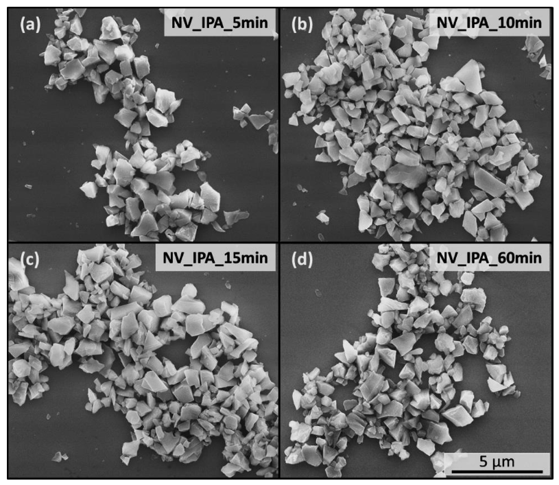
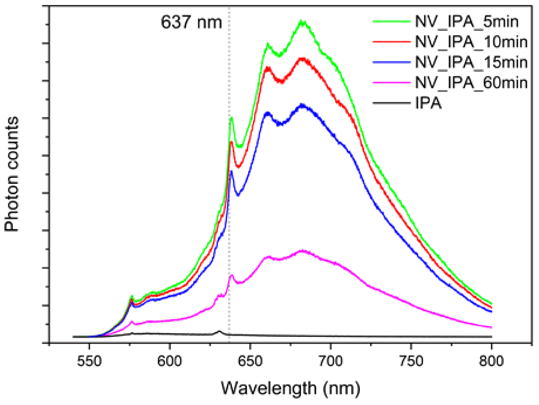
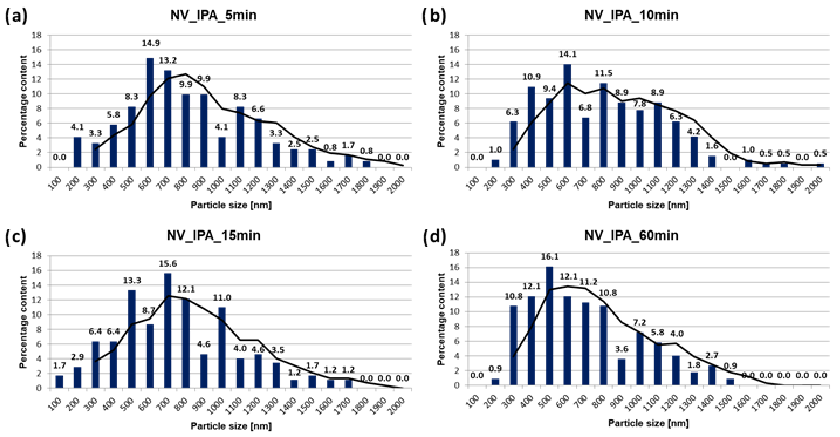
3.1. NV-Rich Nano diamond Particle Parameters

According to the volume-weighted particle size distribution (PSD) measured via dynamic light scattering (DLS), the sizes of the as-received nanodiamond particles were in a range of 300–1500 nm, with 750 nm being the central peak of the distribution. In the present experiment, instead of measuring the particle size distributions in the suspensions with the use of DLS, the SEM images were digitally processed for two reasons. Firstly, the volume-weighed PSD measured via DLS is calculated using the Mie theory, which does not apply accurately if the shapes of the particles are not spherical [24]. Secondly, only the NV-rich nanodiamond particles placed on Si substrates and examined via SEM were selected to be combined with the AFM tip, therefore the more local approach in the analysis of PSD was chosen.
SEM images of the silicon substrates covered with the NV-rich nanodiamonds (Figure 3) show that the particles occur in various sizes, and irregular shapes, which are far from spherical. As a result of the evaporation of the isopropanol, the nanodiamonds gathered into one place, but did not agglomerate into complexes. No residual alcohol was observed in the images. Computer analysis of the particle size distributions was performed based on the SEM images presented in Figure 3. The most suitable NV-rich nanodiamond particles to be placed on the AFM tip are marked in blue. These particles are about 500 nm or less in size and have sharp edges.
Figure 3a depicts the SEM image of the droplet of the NV_IPA_5 min suspension dried on the silicon substrate, while Figure 4a represents the PSD calculated based on that image. The 5 min exposure of the suspension to the ultrasound decreased the particle sizes such that 600 nm particles became the dominant fraction. The particles with 700 nm size became the second most numerous groups. In the sample subjected to the ultrasound for five minutes longer (NV_IPA_10min; Figure 3b and Figure 4b) the 600 nm-sized particles remained the dominant fraction, though their content became slightly (0.8%) lower than in the NV_IPA_5min sample. The total content of particles with dimensions smaller than the central fraction significantly increased (from 21.5% to 27.6%), most likely due to fragmentation of the 700 nm-sized nanodiamonds. Moreover, the total content of the particles larger than 1000 nm decreased. The SEM image of the particles from the NV_IPA_15min suspension is shown in Figure 3c, while its corresponding PSD is presented in Figure 4c. After 15 min of sonication, particles with a size of 700 nm were the most numerous groups. This results from the disintegration of the 900 nm-sized fractions showed a substantial decrease in the content of the 600 nm-sized groups, which gave a significant rise to the particles of 500 nm. As before, the total content of the particles larger than 1 μm decreased. NV_IPA_60min (SEM image in Figure 3d, PSD in Figure 4d) was the only sample in which the nanodiamond particles with a size of 500 nm were the most common fraction. The particles with sizes above 1.5 µm were fully eliminated.
Suspensions prepared in the above-described way exhibit strong fluorescence with the intensity depending on the sonication time. The fluorescence spectra of the NV_IPA_5 min, NV_IPA_10 min, NV_IPA_15 min, NV_IPA_60 min suspensions are presented in Figure 5. The samples were excited with a 532 nm laser (Nd: YAG SHG laser Millenia, 532 nm, Spectra-Physics, Katowice, Poland) at the power level of 0.2 W, while the fluorescence spectra, collected at a 45° angle to the exciting laser beam, were recorded utilising a 0.3 m monochromator (SR303i, Andor, Andora Technology Ltd., Belfast, UK) equipped with a 600 groves/mm grating and ICCD detector (DH740, Andor, Andora Technology Ltd., Belfast, UK). The spectra obtained are characteristic for the NV colour centres in diamond, which are well documented in the literature [25,26].
Each spectrum emitted by the investigated suspensions shows local maxima visible at the wavelengths of 575 and 637 nm, which are zero-phonon lines (ZPLs) of the neutral, and negatively charged NV centres, respectively. The 1st and 2nd phonon sidebands, being the next two local maxima in the spectra, are also clearly visible at about 660 and 680 nm. The intensity of the fluorescence emitted by the suspensions decreases with the increasing duration of the ultrasonic treatment. The PSDs presented in Figure 4 confirm that the ultrasonic disintegration carried out without the use of abrasives enables some reduction of the sizes of NV-rich nanodiamond particles. Comparison of the PSDs shown in Figure 4 with Figure 5 indicates that decreasing the size of the NV-rich nanodiamond particles is associated with the decrease of their fluorescence level, as reported in the literature [27,28]. For every sample, the corresponding fluorescence levels were stable over time and the sonication time does not affect the shape of the spectrum.

3.2. NV-Rich Nanodiamond Particle Parameters

There are many examples of NV-ND applications in optical devices. Here, we focus on a combination of the scanning functionality of AFM with the magnetic and temperature sensitivity of ODMR [29,30].
Figure 6a shows two fluorescence spectra (normalised for better comparison). The black curve is a reference from microdiamond particles with NV colour centres. The red curve comes from the NV-rich nanodiamond particle placed on the AFM tip. The dashed lines show the positions of the NV’s ZPLs. 1 mW, 532 nm laser power was used to excite the reference signal. The 1 mW power appeared to be insufficient to stimulate measurable fluorescence from the NV-rich nanodiamond particle on the AFM tip. After increasing the laser power to 50 mW, the fluorescence spectrum (red line in Figure 6a) became measurable but shifted concerning the reference spectrum (black line in Figure 6a). We attribute the shift to the heating of the sample by the excitation laser. Using the temperature scaling presented in reference [31], we estimated that the spectral shift seen in Figure 6a was related to the tip heating by about 300 °C.
Figure 6b shows two ODMR spectra which demonstrate the effect of the tip heating with a much higher sensitivity than the ZPL shift of Figure 6a. The black spectrum is the reference from nanodiamonds with NV centres while the red curve is from the NV-rich nanodiamond particles on the AFM tips. There is a visible shift to lower frequencies due to the green light heating the sample. This figure also confirms the heating of the AFM tip—about 300 °C [32]. The above results indicate that much lower laser powers and correspondingly higher sensitivity of the detection system should be used to excite a nanodiamond with NV colour centres on an AFM tip.
Figure 6c presents the ODMR spectra corresponding to different magnetic field strengths with the individual signals vertically offset for clarity. The maximum ODMR contrast without magnetic field was 0.7% and reduced to 0.35% after application of the field, consistently with observations of NV ensembles in bulk diamond mono-crystals. The observed spectra in a nonzero magnetic field reflect the fact that the sensing volume contains many NV colour centres oriented in arbitrary directions relative to the direction of the magnetic field. With a small detection volume, the averaging is not complete, hence the observed ODMR spectra are a mixture of some discrete and structureless spectral structures.

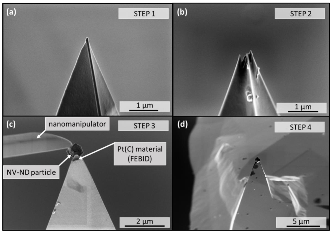
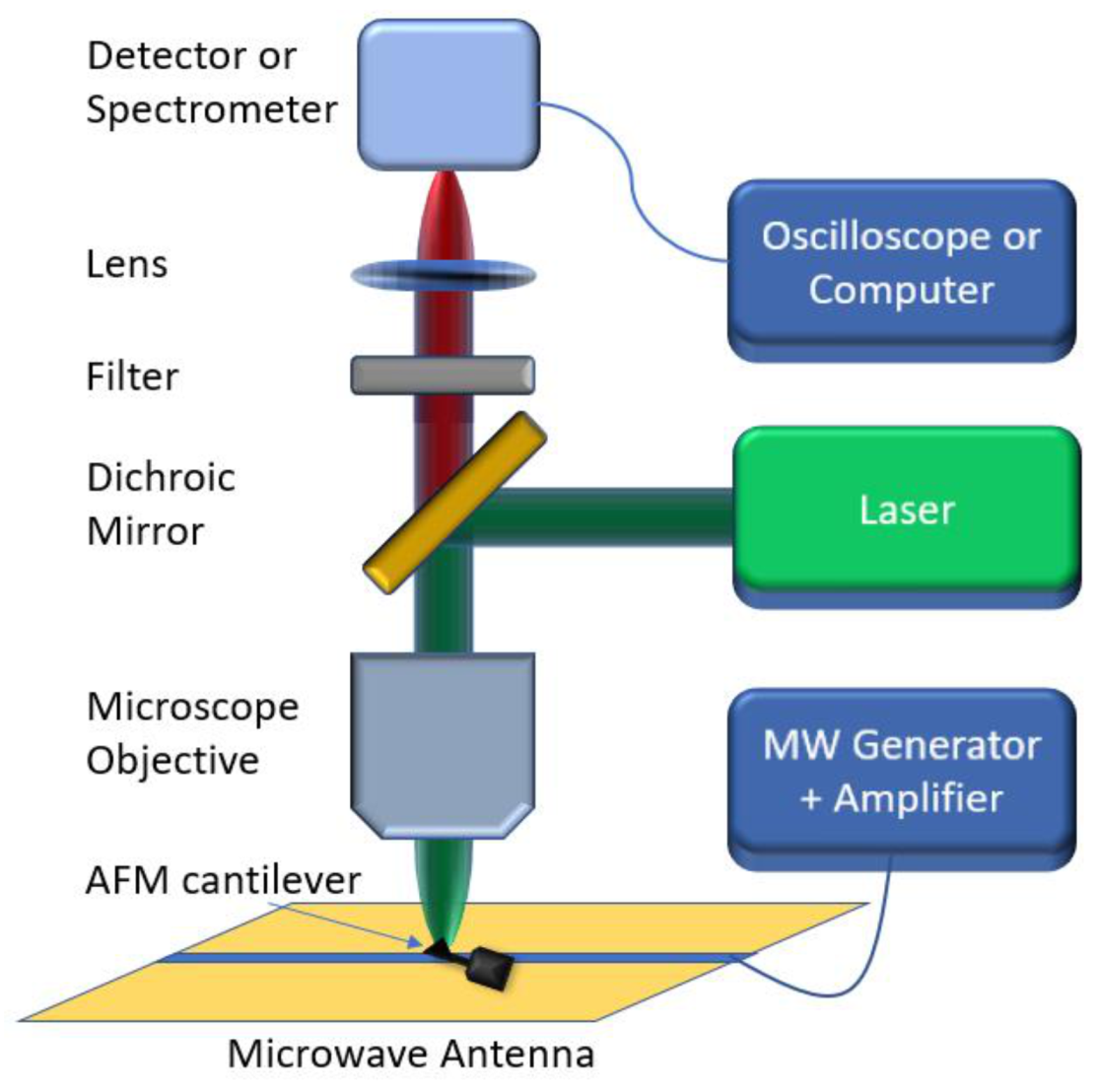
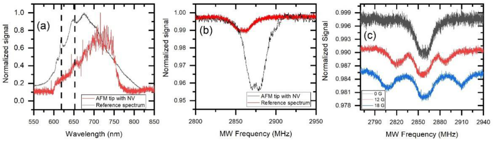
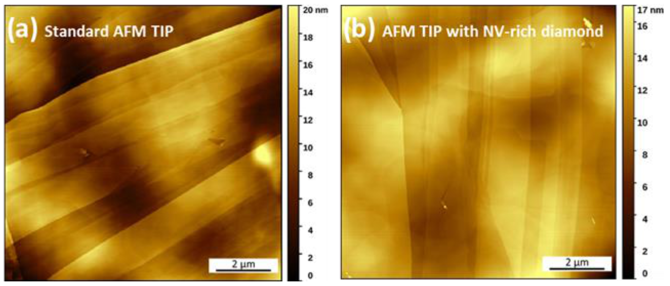
3.3. AFM Cantilevers with NV-Rich Nanodiamond Particle

Four tips with NV-rich nanodiamond particles were chosen for the AFM experiment; three tips were based on the PPP-NCLPt probe (platinum coated AFM tip, fr 146–236 kHz from Nanosensors, Neuchatel, Switzerland) and one on the PPP-EFM probe (platinum coated AFM tip, fr 45–115 kHz from Nanosensors). The typical duration of the experiment was 1 h.
Highly oriented pyrolytic graphite (HOPG) imaging using a typical PPP-ContPt AFM probe (platinum coated AFM tip, fr 6–21 kHz from Nanosensors, Figure 7a), and a NV-rich nanodiamond particle probe (Figure 7b) has been compared. It can be seen that the usage of NV-rich nanodiamond particles did not degrade the imaging capabilities. In both cases, there are visible graphene layers stacked one onto another, forming the graphite sample. The layers end with mono-atomic thickness terraces, which are reproduced without artifacts by both the conventional AFM tip and the NV-rich nanodiamond particle tip. The artifacts characteristic of a damaged tip, such as a double tip or non-sharp images, were not observed during the scanning. Additionally, the obtained RMS roughness was even better for the NV-rich nanodiamond particle tip than for the conventional tip. This proves that using more durable materials with higher abrasion resistance in AFM is promising. The presence of NV centres in the nanodiamond particle makes it a candidate to use in scanning probe magnetometry. The presented method of nanodiamond tip production may result in a higher resolution compared to other recent NV tip development methods [33,34]. This will be an effect of a smaller tip radius.
The smallest recorded variation of the resonant frequency of the AFM tip before and after the imaging was +8 Hz, and the largest was −57 Hz. All values of the cantilevers’ resonant frequencies before and after the experiment are summarised in Table 2. The increase in the resonant frequency is attributed to a decrease in the mass of the probe, whereas a decrease in the resonant frequency is a sign of mass being added [35]. The loss of mass can be attributed to the degradation of the probe during AFM scanning, but this is associated with a decrease in the quality of the recorded image—such a situation was not observed. In contrast, added mass can arise from adsorption of e.g., water or other residues from the sample, or disturbances in the measurement conditions. The authors expect that, considering the added/lost mass of the cantilever caused by its wear, higher resonant frequency changes than those listed in Table 2 (i.e., 100 Hz, which are connected to the recorded image degradation) should be taken into account. A daily routine of the authors shows that the automated resonant frequency finding protocol used in AFM can return differing results, varying about tens of Hz between each attempt. This is within the range of the presented data. The origin of such deviations is the same as for typical spring constant calibration procedures [31,32].

4. Conclusions

In summary, the transfer of an NV-rich diamond particle on an AFM cantilever tip is shown, which provides AFM imaging capabilities. Moreover, it also enables the ODMR spectrum collection with the AFM tip radius resolution. The effective reduction of the size of NV-rich diamond particles by ultrasonic treatment has been demonstrated. The particles thus obtained were placed on the tip of an AFM cantilever. The smallest recorded variation of the resonant frequency of the AFM tip before and after the imaging was +8 Hz, and the largest observed was −57 Hz. Additionally, the ODMR spectrum was collected from the AFM tip revealing resonance maxima shift to lower frequencies due to heating by the green light of the laser excitation. Taking the above into account, it can be stated that the presented method enables the fabrication of AFM probes with NV-rich nanodiamond particles durable enough to perform AFM imaging and ODMR readout.

Author Contributions

Conceptualisation, M.F. and R.B.; methodology, M.F., P.K. and K.S.; validation, M.F., M.J.G. and P.K.; formal analysis, M.J.G. and M.M.; investigation, M.F., P.K. and K.S.; resources, R.B., W.G., A.M.W. and T.P.G.; data curation, M.F., M.M. and K.G.; writing—original draft preparation, M.F., M.J.G., K.G., E.G. and M.M.; writing—review and editing, M.F.; visualisation, M.F., K.G. and M.M.; supervision, R.B., W.G., A.M.W. and T.P.G.; project administration, R.B., W.G. and T.P.G.; funding acquisition, T.P.G., R.B. and W.G. All authors have read and agreed to the published version of the manuscript.

Funding

M.F., M.J.G., K.S., M.M., A.M.W., W.G. and R.B. gratefully acknowledge financial support from the Foundation for Polish Science under the project Team-NET No. POIR.04.04.00-00-1644/18. K.G., P.K., E.G. and T.P.G. gratefully acknowledge financial support from the National Science Centre, Poland under the OPUS grant “Nanometrology of Nottingham cooling effect using operational microelectromechanical systems” (Grant No. 2020/37/B/ST7/03792).

Institutional Review Board Statement

Not applicable.

Informed Consent Statement

Not applicable.

Data Availability Statement

Data sharing is not applicable to this article.

Conflicts of Interest

The authors declare no conflict of interest.

References

  1. Hong, S.; Grinolds, M.S.; Pham, L.M.; Sage, D.L.; Luan, L.; Walsworth, R.L.; Yacoby, A. Nanoscale magnetometry with NV centers in diamond. MRS Bull. 2013, 38, 155–161. [Google Scholar] [CrossRef] [Green Version]
  2. Appel, P.; Neu, E.; Ganzhorn, M.; Barfuss, A.; Batzer, M.; Gratz, M.; Tschöpe, A.; Maletinsky, P. Fabrication of All Diamond Scanning Probes for Nanoscale Magnetometry. Rev. Sci. Instrum. 2016, 87, 063703. [Google Scholar] [CrossRef] [PubMed] [Green Version]
  3. Degen, A. Scanning magnetic field microscope with a diamond single-spin sensor. ACS Appl. Phys. Lett. 2008, 92, 243111. [Google Scholar] [CrossRef] [Green Version]
  4. Taylor, J.M.; Cappellaro, P.; Childress, L.; Jiang, L.; Budker, D.; Hemmer, P.R.; Yacoby, A.; Walsworth, R.; Lukin, M.D. High-sensitivity diamond magnetometer with nanoscale resolution. Nat. Phys. 2008, 4, 810–816. [Google Scholar] [CrossRef]
  5. Maze, J.R.; Stanwix, P.L.; Hodges, J.S.; Hong, S.; Taylor, J.M.; Cappellaro, P.; Jiang, L.; Gurudev Dutt, M.V.; Togan, E.; Zibrov, A.S.; et al. Nanoscale magnetic sensing with an individual electronic spin in diamond. Nature 2008, 455, 644–647. [Google Scholar] [CrossRef]
  6. Rondin, L.; Tetienne, J.-P.; Spinicelli, P.; Dal Savio, C.; Karrai, K.; Dantelle, G.; Thiaville, A.; Rohart, S.; Roch, J.-F.; Jacques, V. Nanoscale magnetic field mapping with a single spin scanning probe magnetometer. Appl. Phys. Lett. 2012, 100, 153118. [Google Scholar] [CrossRef] [Green Version]
  7. Rondin, L.; Tetienne, J.-P.; Rohart, S.; Thiaville, A.; Hingant, T.; Spinicelli, P.; Roch, J.-F.; Jacques, V. Stray-field imaging of magnetic vortices with a single diamond spin. Nat. Commun. 2013, 4, 2279. [Google Scholar] [CrossRef]
  8. Pelz, J.P.; Koch, R.H. Tip-Related Artifacts in Scanning Tunneling Potentiometry. Phys. Rev. B 1990, 41, 1212–1215. [Google Scholar] [CrossRef]
  9. Westra, K.L.; Mitchell, A.W.; Thomson, D.J. Tip Artifacts in Atomic Force Microscope Imaging of Thin Film Surfaces. J. Appl. Phys. 1993, 74, 3608–3610. [Google Scholar] [CrossRef]
  10. Bao, G.W.; Li, S.F. Characterization of Atomic Force Microscopy (AFM) Tip Shapes by Scanning Hydrothermally Deposited ZnO Thin Films. Talanta 1998, 45, 751–757. [Google Scholar] [CrossRef]
  11. Cui, S.; Kim, T.-H.; Ham, U. Influence of the Tip Shape on Scanning Tunneling Luminescence Spectra: Implications for Nanomaterial Characterization. ACS Appl. Nano Mater. 2021, 4, 29–32. [Google Scholar] [CrossRef]
  12. Hartmann, U. Magnetic Force Microscopy. Adv. Mater. 1990, 2, 550–552. [Google Scholar] [CrossRef]
  13. Ruggeri, F.S.; Šneideris, T.; Vendruscolo, M.; Knowles, T.P.J. Atomic Force Microscopy for Single Molecule Characterisation of Protein Aggregation. Arch. Biochem. Biophys. 2019, 664, 134–148. [Google Scholar] [CrossRef]
  14. Canet-Ferrer, J.; Coronado, E.; Forment-Aliaga, A.; Pinilla-Cienfuegos, E. Correction of the Tip Convolution Effects in the Imaging of Nanostructures Studied through Scanning Force Microscopy. Nanotechnology 2014, 25, 395703. [Google Scholar] [CrossRef]
  15. Giessibl, F.J. Advances in Atomic Force Microscopy. Rev. Mod. Phys. 2003, 75, 949–983. [Google Scholar] [CrossRef] [Green Version]
  16. Bogdanowicz, R.; Sobaszek, M.; Ficek, M.; Kopiec, D.; Moczała, M.; Orłowska, K.; Sawczak, M.; Gotszalk, T. Fabrication and Characterization of Boron-Doped Nanocrystalline Diamond-Coated MEMS Probes. Appl. Phys. A 2016, 122, 270. [Google Scholar] [CrossRef] [Green Version]
  17. Shibata, T.; Unno, K.; Makino, E.; Shimada, S. Fabrication and Characterization of Diamond AFM Probe Integrated with PZT Thin Film Sensor and Actuator. Sens. Actuators A Phys. 2004, 114, 398–405. [Google Scholar] [CrossRef]
  18. Kim, J.T.; Choudhury, U.; Jeong, H.-H.; Fischer, P. Nanodiamonds That Swim. Adv. Mater. 2017, 29, 1701024. [Google Scholar] [CrossRef]
  19. Zhou, T.X.; Stöhr, R.J.; Yacoby, A. Scanning Diamond NV Center Probes Compatible with Conventional AFM Technology. Appl. Phys. Lett. 2017, 111, 163106. [Google Scholar] [CrossRef]
  20. Choi, S.; Leong, V.; Alagappan, G.; Krivitsky, L. Enhancing Optical Readout from Diamond AFM Tips for Quantum Nanosensing. ACS Photonics 2018, 5, 4244–4248. [Google Scholar] [CrossRef] [Green Version]
  21. Głowacki, M.J.; Gardas, M.; Ficek, M.; Sawczak, M.; Bogdanowicz, R. Preparation of Fluorescent Nanodiamond Suspensions Using Bead-Assisted Ultrasonic Disintegration. In Proceedings of the 12th Conference on Integrated Optics: Sensors, Sensing Structures, and Methods, Szczyrk-Gliwice, Poland, 3 March 2017; International Society for Optics and Photonics: Bellingham, WA, USA, 2017; Volume 10455, p. 104550E. [Google Scholar]
  22. Thorman, R.M.; TP, R.K.; Fairbrother, D.H.; Ingólfsson, O. The Role of Low-Energy Electrons in Focused Electron Beam Induced Deposition: Four Case Studies of Representative Precursors. Beilstein J. Nanotechnol. 2015, 6, 1904–1926. [Google Scholar] [CrossRef] [Green Version]
  23. Świadkowski, B.; Majstrzyk, W.; Kunicki, P.; Sierakowski, A.; Gotszalk, T. Near-Zero Contact Force Atomic Force Microscopy Investigations Using Active Electromagnetic Cantilevers. Nanotechnology 2020, 31, 425706. [Google Scholar] [CrossRef]
  24. Kreibig, U.; Quinten, M. OPTICAL MATERIALS | Heterogeneous Materials. In Encyclopedia of Modern Optics; Guenther, R.D., Ed.; Elsevier: Oxford, UK, 2005; pp. 446–460. ISBN 978-0-12-369395-2. [Google Scholar]
  25. Manson, N.B.; Hedges, M.; Barson, M.S.J.; Ahlefeldt, R.; Doherty, M.W.; Abe, H.; Ohshima, T.; Sellars, M.J. NV–N+ Pair Centre in 1b Diamond. New J. Phys. 2018, 20, 113037. [Google Scholar] [CrossRef]
  26. Wojciechowski, A.M.; Nakonieczna, P.; Mrózek, M.; Sycz, K.; Kruk, A.; Ficek, M.; Głowacki, M.; Bogdanowicz, R.; Gawlik, W. Optical Magnetometry Based on Nanodiamonds with Nitrogen-Vacancy Color Centers. Materials 2019, 12, 2951. [Google Scholar] [CrossRef] [Green Version]
  27. Shenderova, O.; Nunn, N. Chapter 2—Production and purification of nanodiamonds. In Nanodiamonds; Arnault, J.-C., Ed.; Micro and Nano Technologies; Elsevier: Amsterdam, The Netherlands, 2017; pp. 25–56. ISBN 978-0-323-43029-6. [Google Scholar]
  28. Białobrzeska, W.; Głowacki, J.M.; Janik, M.; Ficek, M.; Pyrchla, K.; Sawczak, M.; Bogdanowicz, R.; Malinowska, N.; Żołędowska, S.; Nidzworski, D. Quantitative fluorescent determination of DNA—Ochratoxin a interactions supported by nitrogen-vacancy rich nanodiamonds. J. Mol. Liq. 2021, 342, 117338. [Google Scholar] [CrossRef]
  29. Chipaux, M.; Tallaire, A.; Achard, J.; Pezzagna, S.; Meijer, J.; Jacques, V.; Roch, J.-F.; Debuisschert, T. Magnetic Imaging with an Ensemble of Nitrogen-Vacancy Centers in Diamond. Eur. Phys. J. D 2015, 69, 166. [Google Scholar] [CrossRef] [Green Version]
  30. Glenn, D.R.; Lee, K.; Park, H.; Weissleder, R.; Yacoby, A.; Lukin, M.D.; Lee, H.; Walsworth, R.L.; Connolly, C.B. Single-Cell Magnetic Imaging Using a Quantum Diamond Microscope. Nat. Methods 2015, 12, 736–738. [Google Scholar] [CrossRef]
  31. Chen, X.-D.; Dong, C.-H.; Sun, F.-W.; Zou, C.-L.; Cui, J.-M.; Han, Z.-F.; Guo, G.-C. Temperature Dependent Energy Level Shifts of Nitrogen-Vacancy Centers in Diamond. Appl. Phys. Lett. 2011, 99, 161903. [Google Scholar] [CrossRef]
  32. Doherty, M.W.; Acosta, V.M.; Jarmola, A.; Barson, M.S.J.; Manson, N.B.; Budker, D.; Hollenberg, L.C.L. Temperature Shifts of the Resonances of the NV Center in Diamond. Phys. Rev. B 2014, 90, 041201. [Google Scholar] [CrossRef] [Green Version]
  33. Guo, M.; Wang, M.; Wang, P.; Wu, D.; Ye, X.; Yu, P.; Huang, Y.; Shi, F.; Wang, Y.; Du, J. A Flexible Nitrogen-Vacancy Center Probe for Scanning Magnetometry. Rev. Sci. Instrum. 2021, 92, 055001. [Google Scholar] [CrossRef] [PubMed]
  34. Orzechowska, Z.; Mrózek, M.; Gawlik, W.; Wojciechowski, A. Preparation and characterization of AFM tips with nitrogen-vacancy and nitrogen-vacancy-nitrogen color centers. Photonics Lett. Pol. 2021, 13, 28. [Google Scholar] [CrossRef]
  35. Lang, H.P.; Berger, R.; Battiston, F.; Ramseyer, J.-P.; Meyer, E.; Andreoli, C.; Brugger, J.; Vettiger, P.; Despont, M.; Mezzacasa, T.; et al. A Chemical Sensor Based on a Micromechanical Cantilever Array for the Identification of Gases and Vapors. Appl. Phys. A 1998, 66, S61–S64. [Google Scholar] [CrossRef] [Green Version]
Figure 1. Development of cantilevers containing NV-rich nanodiamond (NV-ND) particles. (a) step 1—cantilever tip before FIB/SEM processing; (b) step 2—preparation of a slot in the cantilever tip by FIB milling process for attaching the NV-ND particle; (c) step 3—process of transferring by nano-manipulator and mounting of the NV-ND particle onto the hole using Pt(C) material deposited by FEBID technology; (d) step 4—final device with NV-ND particle. Imaging parameters of SEM pictures: 2 kV, 86 pA, tilted stage.
Coatings 11 01332 g001
Figure 2. Schematic of the fluorescence and ODMR measurement setup.
Coatings 11 01332 g002
Figure 3. SEM images of the NV-rich nanodiamond particles deposited on silicon substrates after 5 (a), 10 (b), 15 (c), 60 (d) min of the ultrasonic disintegration. The most suitable NV-rich nanodiamond particles for use on the AFM tip are coloured blue.
Coatings 11 01332 g003
Figure 4. NV-rich nanodiamond particle size distributions in NV_IPA_5 min (a), NV_IPA_10 min (b), NV_IPA_15 min (c), NV_IPA_60 min (d).
Coatings 11 01332 g004
Figure 5. Fluorescence spectra of the NV-rich nanodiamond particles suspended in IPA, after 5, 10, 15, and 60 min of ultrasonic disintegration; the fluorescence spectrum of pure IPA is added as a reference.
Coatings 11 01332 g005
Figure 6. (a) Fluorescence from the NV-rich nanodiamond mounted on an AFM tip (red curve), compared with the reference spectrum from nanodiamond with NV centres (black curve). (b) ODMR spectrum collected from the AFM tip (red curve), and a reference spectrum from the starting, NV-rich nanodiamond particles. (c) ODMR signals for different magnetic field strengths.
Coatings 11 01332 g006
Figure 7. (a) HOPG image obtained using typical AFM probe (PPP-ContPt) without any additional processing. Typical RMS roughness is 3.47 nm (b) AFM image obtained using the AFM probe with NV-rich nanodiamond particle as a scanning tip. Typical RMS roughness is 2.23 nm.
Coatings 11 01332 g007
Table 1. Parameters of the preparation of isopropanol-based suspensions subjected to various durations of ultrasonic treatment.
Name of the SuspensionMass of the NV-Rich Nanodiamond ParticlesVolume of Isopropyl AlcoholTime of Active Operation of Ultrasounds
NV_IPA_5min0.01 g10 mL5 min
NV_IPA_10min0.01 g10 mL10 min
NV_IPA_15min0.01 g10 mL15 min
NV_IPA_60min0.01 g10 mL60 min
Table 2. Changes in the resonant frequency of the investigated probes before and after AFM imaging.
Tipfr before Experiment (Hz)fr after Experiment (Hz)Frequency Difference (Hz)
PPP-EFM63,59863,57325
PPP-NCLPt#1167,262167,319−57
PPP-NCLPt#2159,863159,8558
PPP-NCLPt#3163,726163,70521
Publisher’s Note: MDPI stays neutral with regard to jurisdictional claims in published maps and institutional affiliations.

