Article

Influence of α-Al2O3 Template and Process Parameters on Atomic Layer Deposition and Properties of Thin Films Containing High-Density TiO2 Phases

Institute of Physics, University of Tartu, W. Ostwaldi 1, 50411 Tartu, Estonia
*
Author to whom correspondence should be addressed.
Coatings 2021, 11(11), 1280; https://doi.org/10.3390/coatings11111280
Submission received: 20 September 2021 / Revised: 3 October 2021 / Accepted: 18 October 2021 / Published: 21 October 2021
(This article belongs to the Special Issue Atomic Layer Deposition: Recent Developments and Future Challenges)

Abstract

:
High-density phases of TiO2, such as rutile and high-pressure TiO2-II, have attracted interest as materials with high dielectric constant and refractive index values, while combinations of TiO2-II with anatase and rutile have been considered promising materials for catalytic applications. In this work, the atomic layer deposition of TiO2 on α-Al2O3 (0 0 0 1) (c-sapphire) was used to grow thin films containing different combinations of TiO2-II, anatase, and rutile, and to investigate the properties of the films. The results obtained demonstrate that in a temperature range of 300–400 °C, where transition from anatase to TiO2-II and rutile growth occurs in the films deposited on c-sapphire, the phase composition and other properties of a film depend significantly on the film thickness and ALD process time parameters. The changes in the phase composition, related to formation of the TiO2-II phase, caused an increase in the density and refractive index, minor narrowing of the optical bandgap, and an increase in the hardness of the films deposited on c-sapphire at TG ≥ 400 °C. These properties, together with high catalytic efficiency of mixed TiO2-II and anatase phases, as reported earlier, make the films promising for application in various functional coatings.

Graphical Abstract

1. Introduction

In recent years, the number of attempts at applying TiO2-II, a high-density metastable phase of titanium dioxide (TiO2), has markedly increased [1,2,3,4,5,6,7,8,9,10,11]. This phase had already been observed in high-pressure experiments in the 1960s [12,13,14], and a number of studies, focused on formation and structural studies of TiO2-II [1,2,3,4,5,6,7,8,9,10,11,12,13,14,15,16,17,18,19,20,21,22,23,24,25,26,27,28,29,30,31,32,33,34], have been published since that time. Nevertheless, some properties of TiO2-II need further and more detailed investigation, to widen the applications of this material, for instance, in electronic and optical devices and in functional coatings, which seem to be potential applications of this material.
TiO2-II phase has been prepared from other crystalline phases of TiO2 by high-pressure compression [2,8,12,13,14,15,16,17,18,19,20], ball milling [1,7,21,22], and high-pressure torsion [3,4,5,6]. However, TiO2-II phase has also been obtained in single crystals of limited sizes, grown using a high-pressure hydrothermal method [23,24,25,26]; in powders synthesized using flame techniques [30,31]; and in thin films grown using metalorganic chemical vapor deposition (MOCVD) [29], atomic layer deposition (ALD) [30,31,32,33,34], vapor-liquid-solid [10], and spray pyrolysis [11] methods.
In many cases, TiO2-II has been obtained as an intermediate metastable phase during the anatase to rutile transformation, caused by ball milling [1,7,21,22], and also in thin films deposited at process parameters corresponding to the transition from anatase to rutile growth [31,32,33]. Therefore, it is not surprising that TiO2-II has been observed in crystalline materials, together with anatase and/or rutile [3,4,6,7,22,26,30,31,32,33,34], and that the application of powders and thin films, containing TiO2-II as well as anatase and/or rutile, seems to be more realistic and sometimes more attractive [3,4] than that of pure TiO2-II. For instance, theoretical calculations [35,36] have predicted and experimental studies [3,4] have proved the superior catalytic properties of these kinds of phase combinations. Theoretical studies [35,36] have also demonstrated that some optical parameters of mixed phases cannot be estimated from a simple interpolation of corresponding parameters of pure phases. Thus, further experimental studies of materials containing mixtures of TiO2-II with rutile and/or anatase might be of even higher practical importance than those of phase-pure TiO2-II.
Photocatalysts that are able to produce hydrogen [2,3,4], lithium-ion batteries [8], and supercapacitors with high energy density [9] are some typical applications of materials containing TiO2-II. In these applications, nanocrystalline powders [2,3,4,8] and nanowires [9] have been used. However, the high catalytic activity reported for the materials containing TiO2-II makes these materials attractive for functional coatings as well. Moreover, theoretical studies [37], as well as earlier high-pressure experiments [16,17], have revealed that the bulk modulus of TiO2-II is higher than the corresponding values of rutile and anatase. Thus, the application of TiO2-II is expected to increase the hardness of functional coatings compared to those of the anatase phase that is another catalytically efficient polymorph of TiO2.
As thin films, rather than powders and/or single crystals, are needed in a number of applications, the investigation of the possibility of depositing films containing TiO2-II, and obtaining additional knowledge on the properties of these films, are of significant importance. Previously, TiO2-II has been observed in the thin films deposited by low-pressure MOCVD [29], ALD [30,31,32,33,34], a vapor–liquid–solid method [10], and spray pyrolysis [11]. Among these methods, ALD is the one that allows the most precise (digital) thickness control and is also able to coat surfaces with complex three-dimensional shapes. The application of single crystal c-cut α-Al2O3 (α-Al2O3 (0 0 0 1) or c-sapphire) substrates as templates has had an important role in the formation of TiO2-II in MOCVD [29], as well as in ALD [32,33,34], and improved the reproducibility of the growth process. However, the choice of growth temperature (TG) and precursors also influenced the phase composition of TiO2 films deposited by ALD on α-Al2O3 [32,33]. As a rule, TG ≥ 400 °C has been needed for the formation of TiO2-II on c-sapphire in MOCVD [29] and ALD [32,33]. For comparison, rutile has been grown by ALD at TG ≥ 275 °C on r-cut α-Al2O3 (r-sapphire) [38] and at TG ≥ 225 °C on RuO2 [39].
More detailed studies have revealed that together with TiO2-II, some amount of rutile, lattice-matched to the crystallites with the TiO2-II structure, was formed in the films grown by ALD on c-sapphire [32,33,34]. As a similar combination of phases has been found in natural minerals [40,41,42,43], this kind of TiO2-II/rutile structure seems to be more stable than phase-pure TiO2-II. Comparing the results of earlier ALD studies [32,33,34], one can see, however, that TG, as well as the oxygen precursor used in a TiCl4-based ALD process, had a marked effect on the TiO2-II/rutile ratio in the films. According to Raman spectroscopy and X-ray diffraction (XRD) data, higher TiO2-II concentrations can be obtained in films deposited from TiCl4 and O3 [33,34], rather than from TiCl4 and H2O [32].
In ALD studies, a number of different titanium precursors have been used for the deposition of TiO2 thin films [44,45]. However, at temperatures that are sufficiently high for the formation of significant amounts of TiO2-II in the thin films [31,32,33,34], only few of these precursors [45] ensure the self-limited adsorption in successive surface reactions that the ALD processes are based on [46,47]. For instance, TiCl4 has been used for ALD of TiO2 at temperatures up to 680 °C [32], while another halide, TiI4, has been used for the same purpose at a TG up to 455 °C [38]. For the majority of other titanium precursors, the highest TG that allows the self-limited ALD-type growth of TiO2 is around 400 °C, or even lower [45]. Unfortunately, temperatures of up to 110–130 °C have been needed to volatilize TiI4 in the ALD reactors [38,48]. In contrast, TiCl4 has a sufficiently high vapor pressure, even at room temperature, and for this reason, the TiCl4 source and supply lines of ALD reactors do not need heating. Furthermore, TiCl4-based ALD processes have allowed the deposition of TiO2 films with very high permittivity values [39,49] and coatings with high thickness uniformity on substrates with complex surface shapes [50]. Therefore, TiCl4, as an appropriate titanium precursor for many potential applications of ALD [51,52,53], was also used in our experiments.
Previous studies of films deposited by ALD from TiCl4 and H2O on c-sapphire have shown that the film thickness and precursor doses may influence the TiO2-II to rutile and TiO2-II to anatase ratios in the films [32]. For the films deposited from TiCl4 and O3, no information of this kind has been published yet. The effect of TG on the phase composition of films grown from TiCl4 and O3 on α-Al2O3 has only been studied for relatively thin films [33], while the precursor doses were chosen on the basis of results obtained for ALD of TiO2 on Si substrates [54]. According to the XRD data [33], films containing both TiO2-II and anatase can be grown from TiCl4 and O3 on c-sapphire in a TG range of 300–350 °C. The results of recent studies [3,4,35,36] have shown that this kind of phase combination might be highly efficient in photocatalytic applications. Thus, additional, more detailed, studies would be of marked importance for finding ways to control the transition from anatase to TiO2-II/rutile growth and for obtaining films with different combinations of these phases. In this regard, the TiCl4-O3 process seems to be more promising, as it enables deposition of films with sufficiently high TiO2-II concentrations [34].
In this report, we describe research aimed at revealing the effects of the ALD process parameters and film thicknesses on the growth and properties of TiO2 films deposited at temperatures corresponding to the transition from the anatase to TiO2-II growth and, therefore, allowing the formation of different phase combinations in the films. For a direct comparison of films with different phase compositions, reference films, predominantly containing the rutile and anatase phases, were grown on r-sapphire and SiO2 substrates, respectively. However, the main efforts were focused on the thin films containing TiO2-II, as existing knowledge on the growth and properties of these was limited. Particular attention was paid to the characterization of the optical absorption, bandgap, and hardness, because of the significant importance of these parameters in various applications. As the corresponding information for the films containing TiO2-II phase was disparate or lacking, the results of this work, revealing additional possibilities for manipulating the concentration of TiO2-II and confirming the high hardness of these films, could greatly contribute to the development of functional coatings with superior performance and durability.

2. Materials and Methods

The TiO2 films were grown in a home-made flow-type ALD reactor, described in an earlier publication [55] and also used in our previous research aimed at the growth and characterization of thin films containing the TiO2-II phase [33,34]. In our growth experiments, the films were simultaneously deposited on α-Al2O3 substrates with two different orientations, as well as on a fused silica substrate, to obtain films with different phase compositions, allowing us to study the effect of the phase composition on the optical and mechanical properties of the film. The ALD cycles that were repeated to deposit the films with the required thicknesses included exposure to TiCl4 for 2–5 s, purging for 2–5 s, exposure to O3 for 1–5 s, and another purge for 5 s. Nitrogen (99.999%, AS Linde Gas, Tallinn, Estonia) was employed as a carrier and purge gas. The number of ALD cycles and TG used for deposition of a film was varied from 800 to 2500 and from 250 to 500 °C, respectively. Other deposition process parameters, as well as the substrate pretreatment procedures, were similar to those described previously [33,34].
The crystal structure of the films was characterized by Raman spectroscopy and XRD methods. Raman spectra were measured with an inVia spectrometer (Renishaw, New Mills, UK), using a 514 nm laser beam for excitation. A Smartlab diffractometer (Rigaku, Tokyo, Japan) was employed for XRD studies in the medium resolution point focus, grazing incidence (GIXRD), and high-resolution (HRXRD) modes. For these measurements, Cu Kα1 radiation in the HRXRD mode, and Kα1 and Kα2 radiations in the other modes were used. A polycapillary optics was employed in the medium resolution point focus XRD studies. A more detailed description of these measurements was published previously [34]. The crystalline phases formed in the films were identified using the database PDF-2 2015 of the International Centre of Diffraction Data (ICDD). The film thicknesses, densities, and surface roughness values were determined from X-ray reflection (XRR) patterns (Figure S1), recorded using the same diffractometer.
The refractive index values of the films were determined using a GES5E spectroscopic ellipsometer (Semilab, Budapest, Hungary) and SEA software (Semilab). The incident angles were set at 70, 78, and 75° for measurements of films deposited on SiO2, r-sapphire, and c-sapphire, respectively. A two-layer model was selected for calculation of the refractive index, extinction coefficient, and thickness values from the ellipsometry data. The absorption coefficient (α) values were calculated from the transmission and reflection spectra measured with a V-570 spectrophotometer (Jasco Corp., Tokyo, Japan) at normal incidence in a wavelength (λ) range of 250–750 nm.
Hardness values of the films were measured with a Triboindenter TI980 (Bruker, Billerica, MA, USA) using a Berkovich diamond tip. The device was calibrated in a continuous stiffness measurement mode, measuring a fused silica standard (Bruker), with defined hardness of 9.25 GPa and reduced modulus of 69.6 GPa. The strain rate of 0.05 nm/s and tip vibration frequency (220 Hz) were kept constant during the calibration and the following measurements of films grown on c- and r-sapphire substrates. Calibration validation indicated that the valid displacement range was 10–65 nm. The standard deviations for a single calibration measurement were around 1.5 GPa for modulus and 0.2 GPa for hardness. Thirty separate continuous stiffness measurements were performed on each sample. A maximum drift of 0.05 nm/s was the default acceptance level of a measurement.

3. Results and Discussion

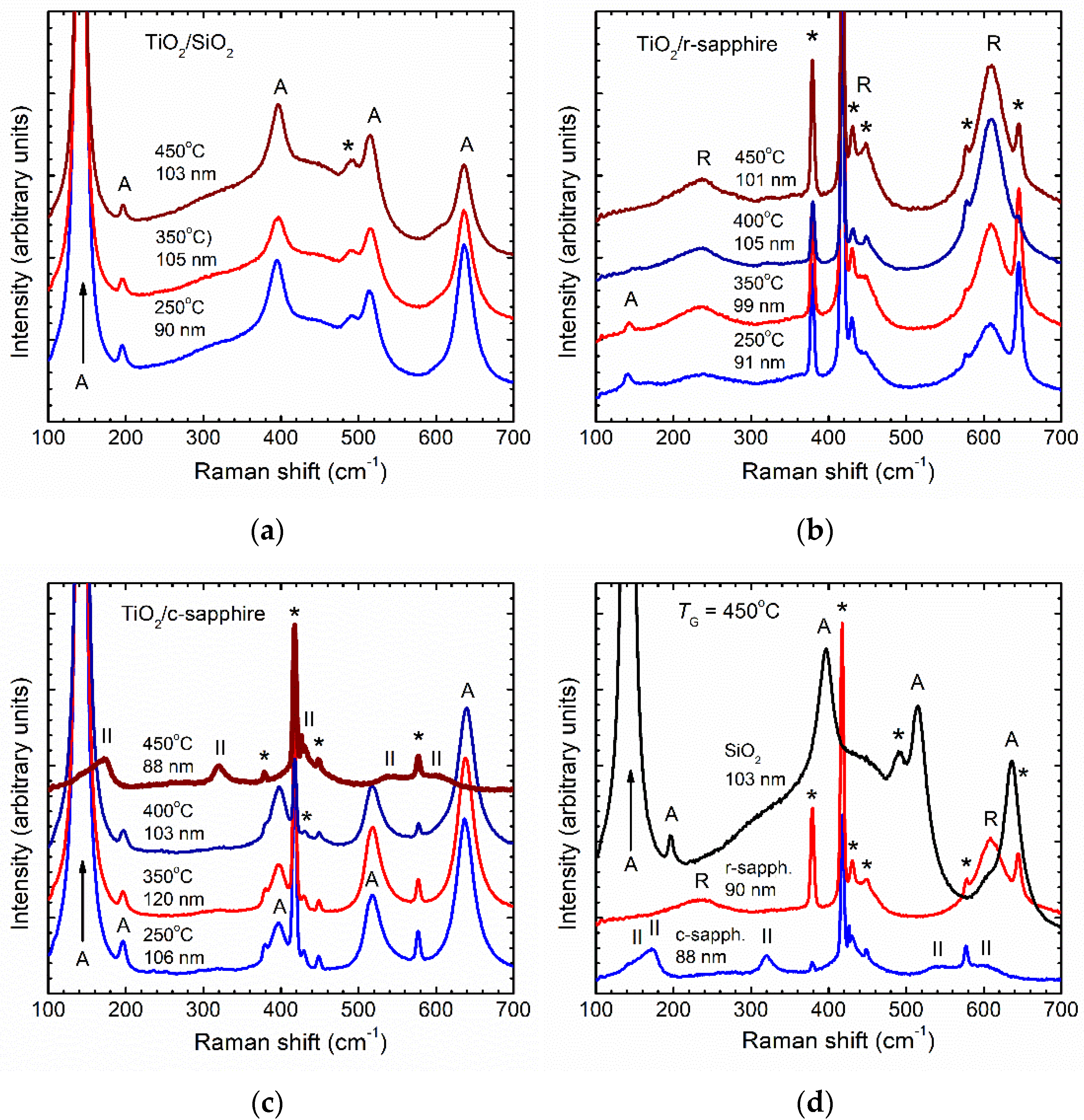
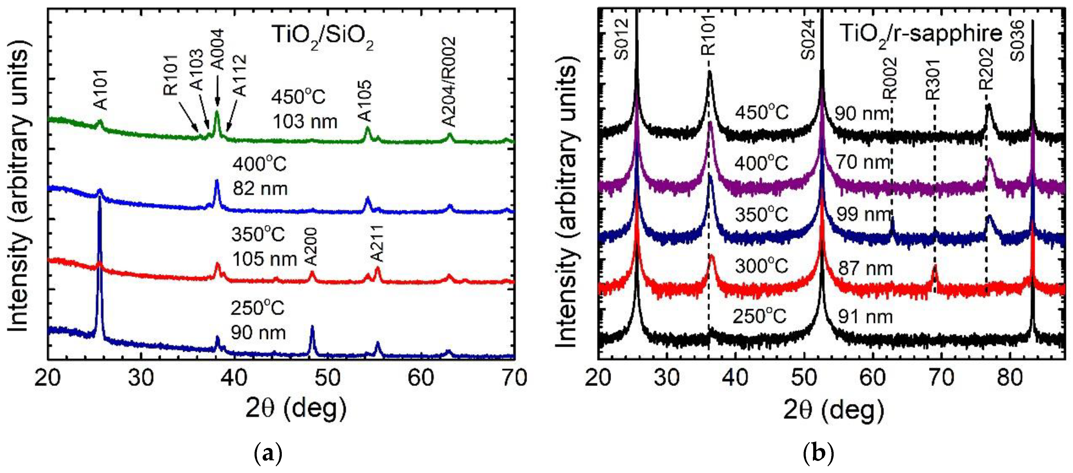
3.1. Effect of Growth Temperature and Film Thickness on Crystal Structure

The influence of TG and film thickness on the phase composition was studied for the films deposited using the cycle times of 2, 2, 5, and 5 s for the TiCl4 pulse, purge, O3 pulse, and another purge, respectively. The Raman spectra of the 90–105-nm thick reference films deposited on SiO2 (Figure 1a) and r-sapphire (Figure 1b) indicated that anatase and rutile, respectively, were formed on these substrates, as had also been observed in previous studies [33,34]. However, a feature visible at around 600 cm−1 in the Raman spectrum of a film grown on SiO2 at 450 °C (Figure 1a) indicated minor amounts of rutile in the film, while traces of anatase were observed in the films deposited on r-sapphire at 250–350 °C (Figure 1b).
According to the Raman spectroscopy data, anatase was predominantly formed in 88–113-nm thick films grown on c-sapphire at TG ≤ 400 °C (Figure 1c). In contrast, only the Raman bands of TiO2-II [8,18,26], together with those of sapphire, dominated in the Raman spectra of the films grown at 450 °C (Figure 1c). Direct comparison of the Raman band intensities, recorded for the films deposited on different substrates at 450 °C, demonstrated that in the case of films with a similar thickness, the Raman scattering of anatase, especially at 143 cm−1, was much stronger than that of rutile and TiO2-II (Figure 1d). Therefore, the absence of the anatase bands in the Raman spectra of the films deposited on c-sapphire at 450 °C (Figure 1c) and the appearance of only a very weak peak in the Raman spectra of the films deposited on r-sapphire at 250–400 °C (Figure 1b) were evidence of negligible or insignificant quantities of anatase in these films. Correspondingly, the formation of marked amounts of TiO2-II was needed to detect this phase by Raman spectroscopy in the films that also contained anatase and/or rutile phases.
Differently from the results depicted in Figure 1, those of our earlier studies showed that TiO2-II, rather than anatase, dominated in the 30 nm thick films deposited on c-sapphire at 400 °C, while the 55-nm thick films deposited on r-sapphire at 250 °C contained significant amounts of anatase in addition to rutile [33]. Probable reasons for this disagreement were the different film thicknesses and/or dissimilar precursor doses used in these two works.
In agreement with the Raman spectroscopy data (Figure 1) and earlier results [33,34], the GIXRD and HRXRD studies of the present work revealed the predominant growth of anatase on SiO2 (Figure 2a) and rutile on the r-sapphire substrates (Figure 2b). The preferential orientation of anatase on SiO2 depended on TG. In the diffraction pattern of the film deposited at 250 °C, the relative intensities of reflections did not differ markedly from those of the powder diffraction database (PDF 84-1286). With the increase of TG, the intensity of the anatase 1 0 1 reflection decreased and that of the 0 0 4 reflection significantly increased, showing notable changes in the preferential orientation of crystallites. In addition, minor traces of rutile appeared in the film deposited on SiO2 at 450 °C, as indicated by the weak rutile 1 0 1 reflection in the corresponding diffraction pattern at 36.2° (Figure 2a). These structural changes were very similar to those described in more detail in the case of films deposited on silicon substrates in the same TG range [54,56]. This similarity was not surprising, because the native SiO2 layer formed on the silicon substrates before or during ALD made the TiO2 growth processes on the silicon and amorphous SiO2 substrates comparable to each other.
The rutile films obtained on r-sapphire exhibited the preferential (1 0 1) orientation (Figure 2b). However, the orientations 3 0 1 and 0 0 1 were also observable in the films deposited at 300 and 350 °C (Figure 2b). The substrate-controlled (1 0 1) orientation of the rutile growth on r-sapphire is well-known and thoroughly characterized [38,57,58]. The presence of the additional orientations of rutile on r-sapphire, for instance in the films deposited on r-sapphire at 350 °C from TiCl4 and H2O [59], had also been observed previously, and for this reason, was not of the main interest in this work.
The HRXRD studies of the films deposited on c-sapphire (Figure 3) confirmed the results of the Raman spectroscopy measurements (Figure 1c). The diffraction patterns of the films deposited at 250 °C exhibited only the reflections (at 37.9°–38.1°, 38.7°, and 82.7°) that were indexed as the 0 0 4, 1 1 2, and 2 2 4 reflections of anatase (Figure 3). Additional reflections appeared in the diffraction patterns of the 44–63 nm thick films deposited at TG ≥ 300 °C (Figure 3a). The latter reflections were indexed as the 0 0 8 reflection of anatase (the reflection peaking at 80.6°) and the 2 0 0 and 4 0 0 reflections of TiO2-II or highly distorted rutile (the reflections peaking at 39.8° and 85.7°). However, the 39.8° and 85.7° reflections were absent or very weak in the diffraction patterns of the thicker (104–120 nm) films deposited at 300–350 °C (Figure 3b). Thus, TG ≥ 400 °C were needed to obtain significant amounts of TiO2-II and/or rutile in the films with these thicknesses (Figure 3b). It is also worth noting that no anatase reflections, except for the 0 0 4, 1 1 2, 0 0 8, and 2 2 4 reflections, were observed in a 2θ range of 20°–88° in the HRXRD patterns of the films deposited on c-sapphire. Thus, owing to the template effect of c-sapphire, anatase with the preferential (0 0 1) and (1 1 2) orientations grew on these substrates at 250–400 °C.
The (0 0 1) and (1 1 2) orientations of anatase on c-sapphire were observed and analyzed by Chang et al. [29], Chen et al. [60], and Roch et al. [61] in epitaxial films grown by metalorganic chemical vapor deposition [29,60] and reactive direct-current magnetron sputtering followed by annealing at 600 °C [61]. Epitaxial relationships A(1 1 2)[1 1 0] || S(0 0 0 1)[2 ͞1 ͞1 0], A(1 1 2)[1 ͞1 0] || S(0 0 0 1)[1 ͞1 0 0] and A(0 0 1)[1 ͞1 0] || S(0 0 0 1)[1 ͞1 0 0] were reported for these two orientations of anatase [61]. Therefore, it was not surprising that anatase with the same out-of-plane preferential orientations was obtained in our experiments as well.
As could be concluded from the HRXRD reflection positions of the films deposited on c-sapphire at TG ≥ 300 °C (Figure 3), TiO2-II rather than rutile was formed together with anatase in these films. However, the previous studies, which included φ-scanning and high-resolution reciprocal space mapping performed for the films deposited at TG ≥ 425 °C, demonstrated that rutile, lattice-matched to TiO2-II, was also formed in the films that were deposited on c-sapphire and showed the reflections peaking at 39.7° and 85.4° [32,33]. For the independent determination of TiO2-II and rutile in the films grown in this work, the XRD reflections from the (1 1 0) planes of (1 0 0) oriented rutile (reflection R1 1 0 in Figure 4) and from the (1 1 1) planes of (1 0 0) oriented TiO2-II (reflection II1 1 1 in Figure 4) were recorded using the sample tilting and point focus optical setup for the XRD device. Additionally, the anatase 1 0 1 reflection (A1 0 1 in Figure 4) as a reference was measured for (0 0 1) oriented anatase. All three reflections were present in the XRD patterns of the films deposited at 300 °C (Figure 4a) and 400 °C (Figure 4b). Therefore, anatase, TiO2-II, and rutile were simultaneously formed in the films deposited on the c-sapphire in this TG range.
The results, depicted in Figure 5, confirmed those in Figure 3 and demonstrated that in a TG range of 350–400 °C, the increase of the film thickness on the c-sapphire substrates resulted in a more preferential growth of anatase compared to that of TiO2-II and/or rutile. Therefore, the template effect, leading to the growth of the high-density phases, was extended to the relatively small film thicknesses at these temperatures. However, at TG ≥ 450 °C, it was possible to deposit up to 88-nm thick films that were free of anatase inclusions, as proven by the HRXRD patterns (Figure 3b) and Raman spectra (Figure 1c and Figure 6a). Moreover, the Raman studies did not reveal any changes in the TiO2-II to rutile concentration ratios, when the thicknesses of the films deposited at 450 °C increased from 14 to 88 nm (Figure 6a). In contrast, the thickness increase (from 24 to 56 nm) of the films deposited on c-sapphire at 500 °C caused an increase in the relative intensity at 600–620 cm−1 (Figure 6b), where an intense Raman band of rutile was located (Figure 1b,d). Similar changes in the Raman spectra were observed with increasing thickness of the TiO2 films grown at 500 °C on c-sapphire from TiCl4 and H2O [32]. The increase in the rutile content with increasing film thickness was shown to be the reason for these changes in the Raman spectra [32]. Hence, also taking into account the result that the increase in the film thickness led to an increase in the anatase content at TG ≤ 400 °C, one could conclude that the TG range allowing growth of the TiO2-II phase became narrower with increasing film thickness.
One interesting effect was that the intensities of the TiO2-II/rutile 2 0 0 and 4 0 0 reflections, recorded for the films deposited at 300 and 350 °C, were markedly decreased with increasing film thickness (Figure 3 and Figure 5a). Consequently, the TiO2-II phase, formed in the initial growth stage, transformed to another phase during the following growth process. It should be noted in this connection that there is a relatively good matching of (1 1 2) plane of anatase and (1 0 0) plane of TiO2-II, allowing phase transitions between these 2 phases in the [1 1 2] direction of anatase and [1 0 0] direction of TiO2-II, as suggested by theoretical studies [35,36]. This kind of lattice-matching should also enable the epitaxial growth of these phases on each other.
Comparing the lattice parameters of anatase and TiO2-II, Zhao et al. [35] estimated that in a structure containing four layers of TiO2-II on one side of a junction and four layers of anatase on the other side, the 2D unit cell area in the (0 0 1) plane of TiO2-II would increase by 1.90% and that in the (1 1 2) plane of anatase would decrease by 6.24% compared to those in the bulk materials. With the increase in the amount of anatase, the strain in the anatase decreases, while the tensile strain in TiO2-II increases [35]. Therefore, it is possible that the increase in the lattice strain in TiO2-II can cause the phase transition to anatase, when the amount of anatase in the crystallites containing both phases reaches a critical level. The similarity in the atomic arrangements on the (1 1 2) plane of anatase and on the (1 0 0) plane of TiO2-II can be also considered as a reason for the faster decrease in the amount of the (1 1 2) oriented anatase compared to that of the (0 0 1) oriented anatase with the increase in the amount of TiO2-II in the films (Figure 3). Owing to this similarity, the (1 1 2) oriented anatase and (1 0 0) oriented TiO2-II can occupy the same areas on the surface of c-sapphire and, therefore, inhibit the growth of each other.
To characterize the crystallization processes in more detail, crystallite sizes (Figure 7) were calculated from the full width at half maximum (FWHM) values of the XRD reflections. The Scherrer equation [62] was used to calculate the X-ray apparent crystallite sizes in the direction perpendicular to the corresponding lattice planes. For the films deposited on c-sapphire, the crystallite sizes were determined for the (1 0 0) oriented TiO2-II/rutile, (0 0 1) oriented anatase, and (1 1 2) oriented anatase, while for the films grown on r-sapphire, the crystallite sizes were determined for the (1 0 1) oriented rutile (Figure 7).
In the films that contained significant amounts of anatase and in the rutile films deposited on r-sapphire, the XRD crystallite sizes were markedly smaller than the thicknesses of the respective films (Figure 7). In contrast, the crystallite sizes reached values that were close, or equal, to the thicknesses of the films, where the (1 0 0) oriented TiO2-II/rutile started to dominate (Figure 3 and Figure 7). Therefore, in the latter films, the crystallites grew from the film/substrate interface up to the film surface without interruption. This kind of growth, together with the highly developed preferential orientation of crystallites in these films [33,34], was the reason why Pendellösung oscillations appeared on the shoulders of the 39.8 and 85.7° reflections in the diffraction patterns of the films deposited on c-sapphire at TG ≥ 400 °C (Figure 3 and Figure 5). The crystallite sizes of anatase grown on c-sapphire and those of rutile formed on r-sapphire were significantly smaller compared to the film thicknesses. Moreover, the orientations of the latter crystallites scattered significantly [33,34]. Correspondingly, no Pendellösung oscillations appeared at the 0 0 4, 1 1 2, 0 0 8, and 2 2 4 reflections of anatase (Figure 3 and Figure 5), and at the 1 0 1 reflection of rutile (Figure 2b).

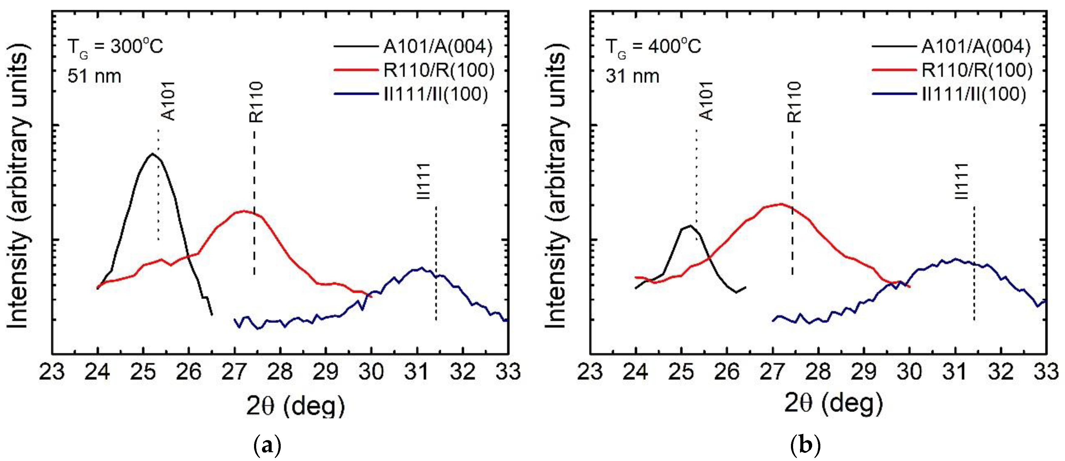
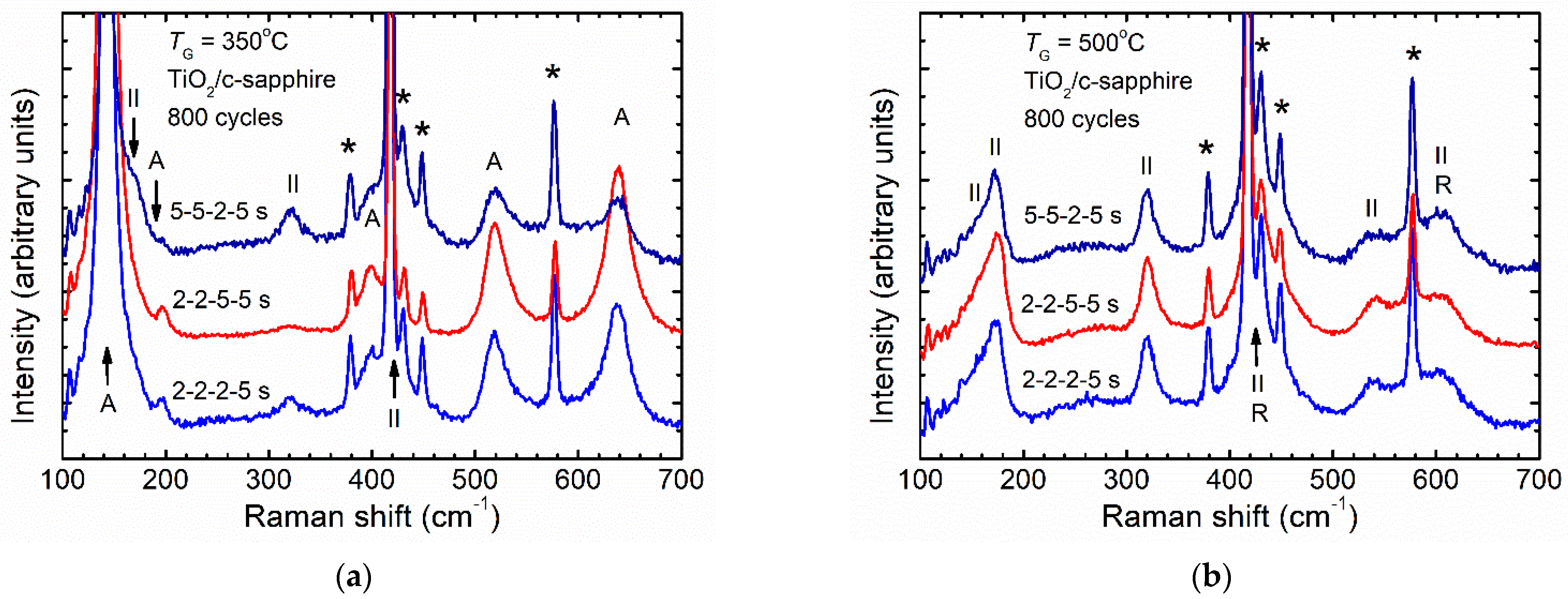
3.2. Effect of ALD Process Time Parameters on Phase Composition

The effect of ALD process time parameters on the phase composition was characterized for the films deposited on c-sapphire at 350, 400, and 500 °C, because significant amounts of different phases were obtained, or anticipated to be obtained, in the films at these temperatures. Therefore, the changes in the phase composition caused by the variation of the deposition process time parameters were expected to be sufficient for reliable detection.
According to the results of HRXRD characterization of the films grown at 400 °C (Figure 8a), an increase in the TiCl4 pulse duration from 2 to 4 s, an increase in the first purge period from 2 to 5 s, and, especially, the decrease in the O3 pulse duration from 5 to 2 s resulted in a considerable reduction of the relative amount of anatase in the thinner (29–31 nm) films. This result was in line with those of earlier studies, indicating that the O/Ti atomic ratios below 2 in the solid phase were beneficial for the formation of TiO2-II [63,64]. Unexpectedly, the reduction of the O3 pulse duration did not cause a decrease in the relative amount of anatase in the thicker (>100 nm) films (Figure 8b). Thus, the precursor doses had a stronger effect on the initial stage of the crystallization processes, rather than on the growth of crystallites with larger sizes.
Raman spectroscopy studies of the films deposited at 350 °C corroborated the results of HRXRD measurements. The increase in the intensities of the TiO2-II Raman bands peaking at 173 and 320 cm−1, and the decrease in the intensities of the anatase bands peaking at 197, 398, 518, and 639 cm−1 (Figure 9a) indicated that both the decrease in the O3 pulse duration from 5 to 2 s and the following increase in the TiCl4 pulse and the first purge durations from 2 to 5 s caused an increase in the relative amount of TiO2-II in the films.
A somewhat different dependence of the phase composition on the process time parameters was observed in the case of films deposited on c-sapphire at 500 °C. The Raman spectra of these films (Figure 9b) demonstrated that the decrease in the O3 pulse duration, as well as the increase in the TiCl4 pulse duration and the following purge time, which supported growth of TiO2-II at 350 °C, inhibited the growth of this phase compared to that of rutile at 500 °C (Figure 9b). Thus, the optimization of the process time parameters allowed us to reduce the temperature for the most efficient growth of TiO2-II, but did not widen the temperature window of the preferential TiO2-II growth considerably.
It should also be noted that significant changes in the process time parameters listed in this section caused only minor changes in the growth per cycle (GPC). For instance, the thicknesses determined by XRR for the films grown by applying 800 ALD cycles at 350 °C (Figure 9a), 400 °C (Figure 8a), and 500 °C (Figure 9b) were 38–44, 29–31, and 24–26 nm, respectively. Consequently, all films were deposited in the self-limited ALD mode or very close to that. Nevertheless, the variation of the cycle time parameters led to marked changes in the crystal structure of the thinner films (Figure 8a and Figure 9).

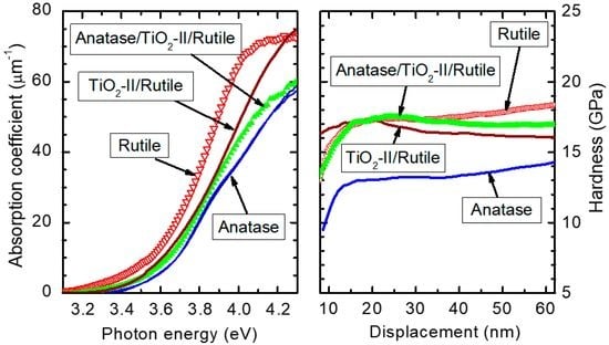
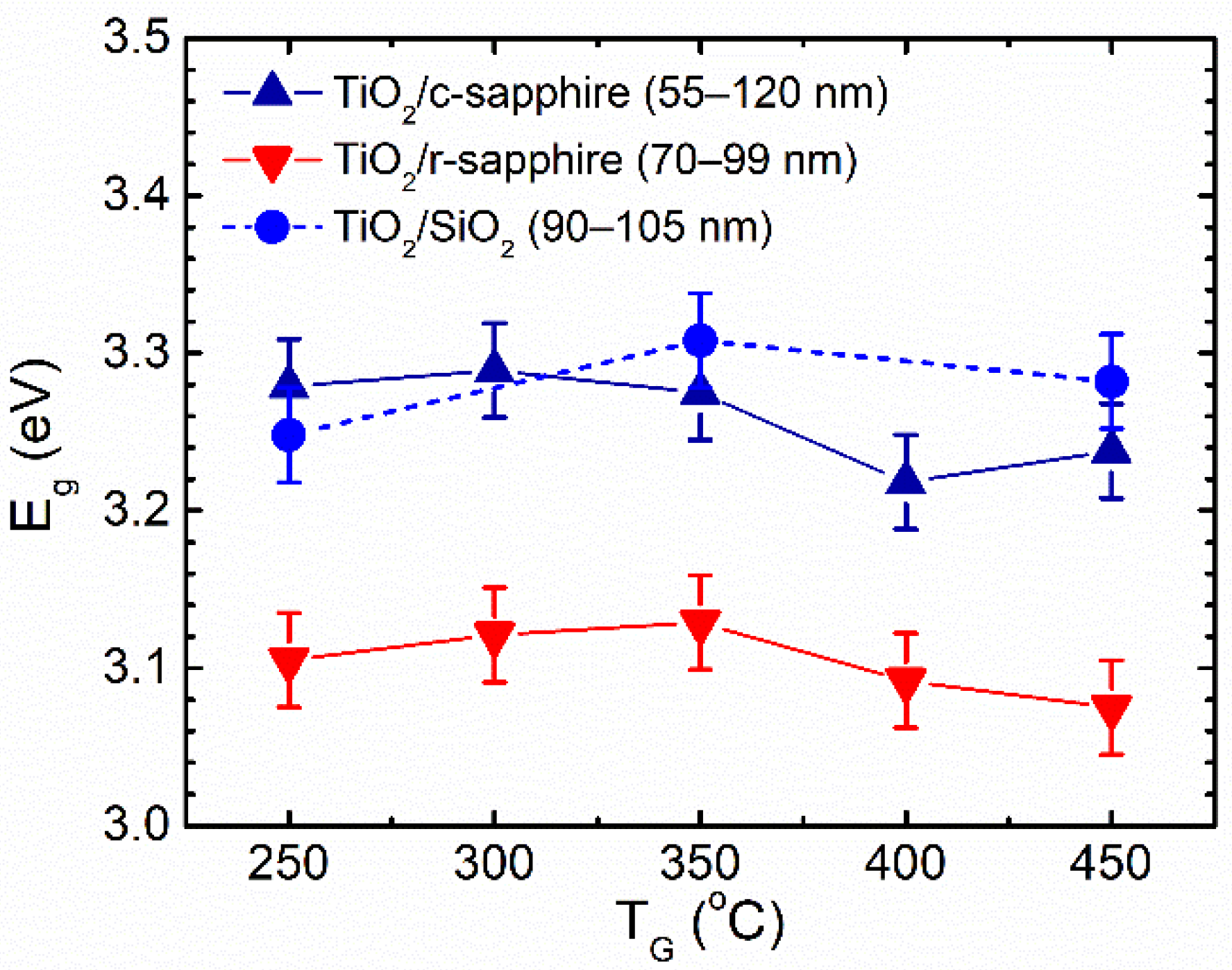
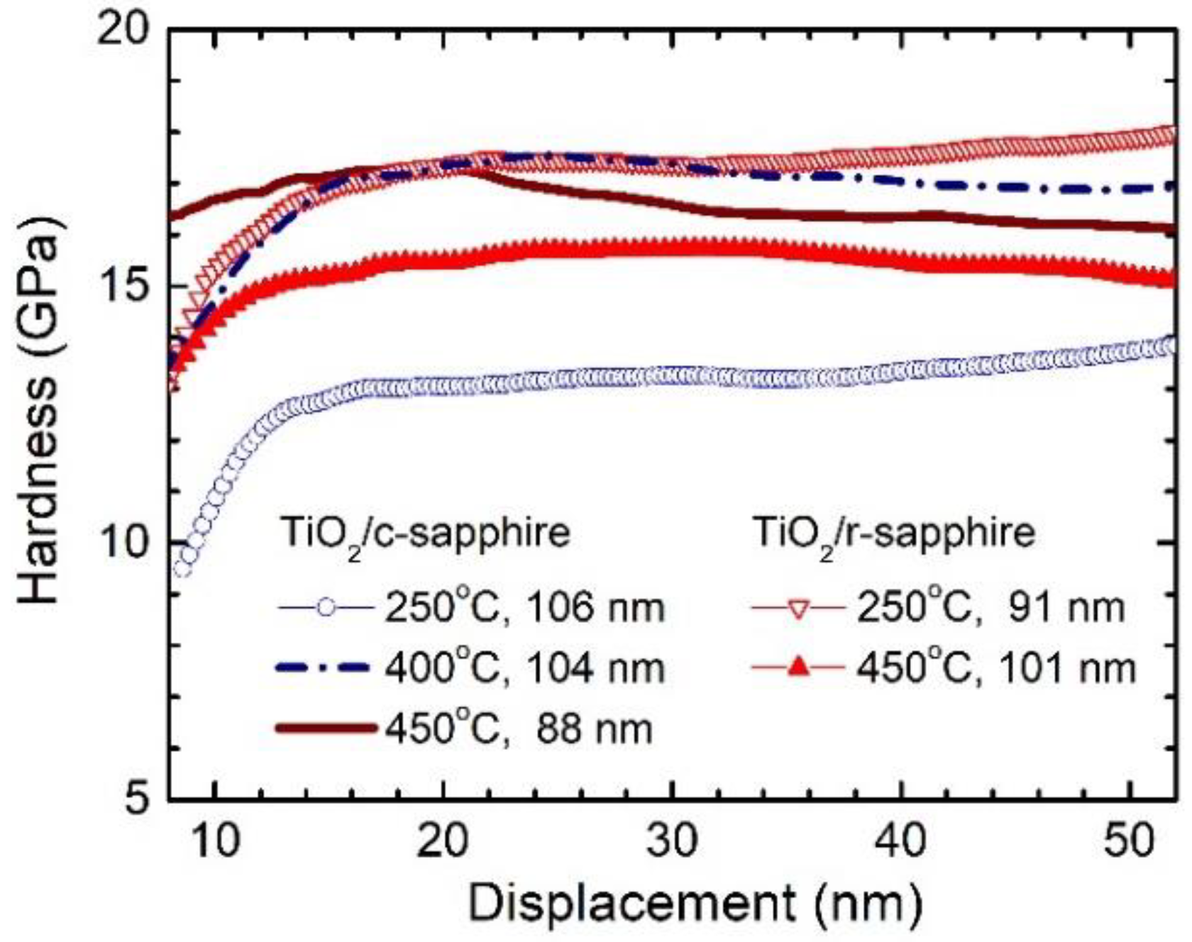
3.3. Influence of Phase Composition on the Growth Rate and Properties of Films

The results presented in Figure 10a demonstrate that GPC, which did not depend greatly on the precursor pulse durations varied from 2 to 5 s, depended considerably on the film thickness, substrates, and TG. Most significantly, the film thickness influenced GPC at the lowest TG used, while the highest GPC values were obtained on the c-sapphire substrates. An explanation for the latter effect was the (0 0 1) orientation of the anatase supported by these substrates (Figure 3). Earlier studies revealed that in TiO2 films grown by ALD on substrates that did not control the orientation of crystal structure, a (0 0 1) orientation of anatase was developed during the growth process [54,56]. Consequently, the ALD growth was faster for crystallites with this orientation, rather than those with other orientations. Therefore, it is not surprising that the growth of anatase was faster on the c-sapphire substrates that supported the development of the (0 0 1) orientation.
With a TG increase from 300 °C to higher values, the GPC decreased on all substrates used. However, the decrease was smaller on the SiO2 substrates where predominantly anatase grew, at all temperatures used in this work. On the c-sapphire substrates, the most significant changes in the crystal structure appeared with a TG increase from 350 to 450 °C (Figure 2 and Figure 3). Correspondingly, the biggest decrease in GPC of the films deposited on those substrates was also observed in this TG range. As a result, the GPC values of the films deposited on different substrates at 450–500 °C markedly differed from each other; the highest values being for the anatase films deposited on SiO2, and the lowest values for the TiO2-II/rutile films grown on c-sapphire (Figure 10a).
Expectedly, the lowest surface roughness values determined by XRR were obtained for the films that were deposited on c-sapphire at 450–500 °C and on r-sapphire at 350–450 °C (Figure 9b). These films exhibited also a well-developed preferential (1 0 0) orientation of lattice-matched TiO2-II and rutile on c-sapphire (Figure 3) and the (1 0 1) orientation of rutile on r-sapphire (Figure 2b). Interestingly, the thicker films deposited on c-sapphire at 400 °C showed the highest surface roughness values (Figure 10b). At other TG used, the films with the highest surface roughness values grew on the SiO2 substrates. No considerable effect of the thickness on the surface roughness was observed for the films grown on c-sapphire at 450 °C and on r-sapphire at 250–450 °C. Therefore, the preferential orientation of crystallites and the absence of the anatase phase in the films seemed to be a precondition for obtaining films with smooth surfaces.
The very high roughness values of thicker films deposited on c-sapphire at 400 °C (Figure 10b) were probably related to the transition from anatase to TiO2-II/rutile growth at this temperature. A similar increase in the surface roughness was earlier observed in the case of TiO2 films grown at temperatures corresponding to the transition from amorphous to anatase growth with increasing TG [65,66], and in the case of aluminum–titanium oxide films in the composition ranges corresponding to the transition from anatase to amorphous growth with increasing Al concentration [55]. In all cases, the most probable reason for this performance was the simultaneous presence of domains with very different growth rates in the films [65,66]. The same effect, based on the higher growth rate of anatase and lower growth rate of (1 0 0) oriented TiO2-II/rutile, was likely a reason for the surface roughening of the thicker films deposited on c-sapphire at 400 °C (Figure 10b).
The densities of the films (Figure 10c) were in relatively good correlation with the crystal structure formed. Expectedly, the densities of the anatase films deposited on SiO2 were somewhat smaller than the XRD database values of anatase (PDF 84-1286). The difference was obviously due to the contribution of the surface and interface layers with lower density, as well as due to the limited packing density of the crystallites with different orientations in the polycrystalline films formed on the amorphous SiO2 substrates (Figure 2a). For comparison, films with somewhat higher densities grew on c-sapphire at 250–350 °C (Figure 10c), although anatase was also the dominating phase in these films (Figure 1c and Figure 3). The higher densities of the latter films were likely related to the higher packing density of crystallites with well-developed preferential orientations and the inclusion of TiO2-II and rutile phases in the films (Figure 3 and Figure 4). With the increase of TG from 350 to 450 °C, the density of the films grown on c-sapphire increased and reached values comparable to, or even higher than, those of the rutile films deposited on r-sapphire (Figure 10c).
The densities of the rutile films deposited on r-sapphire also increased with the TG increase from 250 to 450 °C. This increase was evidently due to some changes in the phase composition, as indicated the disappearance of a weak anatase band and the increase in the intensities of the rutile Raman bands with the TG increase from 250 to 400 °C (Figure 1b). However, the increase in the densities of the films deposited on r-sapphire was smaller than that observed with increasing TG for the films deposited on c-sapphire, as expected.
The refractive index values, measured at λ = 633 nm for the films deposited on the c-sapphire substrates, and the densities of these films, similarly depended on TG (Figure 10c,d). In agreement with the results of earlier studies [34], the refractive index values of the TiO2-II/rutile films grown on c-sapphire at 400–450 °C were somewhat higher than the refractive indices of the rutile films grown on r-sapphire at the same temperatures (Figure 10d). An unexpected result was that, differently from the densities, the refractive indices of the rutile films deposited on r-sapphire decreased with the increase of TG from 250 to 400 °C. Most probably, this result was related to the optical anisotropy of rutile [67,68] and changes in the orientations (Figure 2b) and sizes (Figure 7) of crystallites with the TG increase. Therefore, it is possible that the extraordinary refractive index, having higher values than the ordinary one [67,68], more significantly contributed to the results in the films with a less developed preferential orientation and obtained at lower temperatures.
Absorption spectra were calculated from the optical transmission (Figure 11a) and reflection (Figure 11b) spectra, using the formula α = (1/d)ln[(1 − R)/T] [69,70], where α is the absorption coefficient, d is the film thickness, R is the reflection, and T is the transmission. The transmission spectra (Figure 11a) snd the absorption spectra (Figure 11c) confirmed that the films were highly transparent at wavelengths ≥400 nm (at the photon energies hν ≤ 3.1 eV). In this spectral range, the absorption coefficient values did not exceed the experimental uncertainty, which was around 0.5 μm−1. In the spectral range of medium and strong absorption (at hν ≥ 3.1 eV), the absorption spectra of the 106–120-nm thick films deposited on c-sapphire at 250–350 °C (Figure 11c) exhibited, at 3.9 eV, a feature that was typical for anatase [34,68]. In addition, the α values were similar to those reported for the anatase films deposited on SiO2 and LaAlO3 substrates and for the anatase single crystals in previous studies [34,68]. This was an expected result, because the anatase phase was the dominant one in the films deposited on c-sapphire at 250–350 °C (Figure 1c and Figure 3).
Considerable changes in the absorption spectra of the films deposited on c-sapphire appeared when the TG was increased from 350 to 450 °C, and TiO2-II and rutile, instead of anatase, started to dominate in the films (Figure 3b). This increase in TG led to considerable changes in the shapes of the absorption spectra, especially at hν > 3.85 eV (Figure 11c). Nevertheless, these changes in the phase composition caused only minor changes in the bandgap values determined from the (αhν)1/2 versus hν curves (Figure 11d), using the Tauc method and corrections suggested by Makula et al. [71]. As was assumed, the bandgap values of the films that were grown on c-sapphire at 250–350 °C and on the SiO2 substrates and that mainly contained the anatase phase were very close to each other (Figure 12). The bandgap energy of the films deposited on c-sapphire decreased considerably, from 3.29 to 3.22 eV, with the increase of TG from 300 to 400 °C (Figure 12), when significant amounts of TiO2-II/rutile appeared in the films (Figure 1c and Figure 3). However, even the reduced bandgap values were markedly higher than those of rutile (Figure 12). These results were in agreement with the experimental data of Ohta et al. [19], Murata et al. [2], and Pushpa et al. [11], as well as the theoretical calculations of Zhao et al. [35].
Markedly lower bandgap values, ranging from 2.2 to 3.0 eV, have been reported for powder materials that contained TiO2-II due to the treatment of the materials using the high-pressure torsion [3,5,6], ball milling [7], and hydrogenation [9] methods. These kinds of differences in the bandgap values of a material prepared with different processes need further studies. On the basis of the present data, one can only speculate that the generation of oxygen vacancies and/or defects in some material treatment processes [6,9] could be the reason for the additional bandgap narrowing.
The hardness values determined by the nanoidentation method (Figure 13) depended on the phase composition of the films. The highest values (17.0–17.5 GPa at tip displacements of 15–20 nm) were obtained for the rutile films deposited on r-sapphire at 250 °C, and also for the films deposited on c-sapphire at 400–450 °C (Figure 13). Markedly lower hardness values (15.2–15.5 GPa) were measured for the rutile films deposited at 450 °C. The decrease in the hardness of the rutile films with increasing TG was probably related to the differences in the crystallite sizes [72].
According to the XRD data, the crystallite sizes were as small as 9 nm in the rutile films deposited on r-sapphire at 300 °C (Figure 7), while the crystallites were evidently even smaller in the films grown at 250 °C, as the XRD reflections of these films were too weak and too wide for the reliable determination of the crystallite sizes. Moreover, the Raman spectroscopy studies revealed minor amounts of anatase in these films (Figure 1b). Most likely, the films also contained some amount of the amorphous phase, as it was possible to conclude on the basis of the lower Raman band intensities of these films compared to the corresponding intensities of the films deposited at higher temperatures (Figure 1b). Therefore, the high hardness values of the films deposited on r-sapphire at 250 °C were probably related to the formation of a nanocrystalline composite that also contained an amorphous component.
With the TG increase to 450 °C, the crystallite sizes in the rutile films increased to 23 nm (Figure 7). Correspondingly, the hardness decreased from 17.5 to 15.5 GPa at a tip displacement of 20 nm. It should be noted that similar decrease in hardness values (from 19 to 15 GPa with the increase in crystallite sizes from 10 to 22 nm) has been reported for rutile films deposited by magnetron sputtering [72]. In agreement with the results of Kulikovsky et al. [72], the lowest hardness values were measured in our studies for anatase films (Figure 12). The hardness values obtained for the anatase films in our nanoidentation measurements (13 GPa at tip displacements of 15–20 nm) were higher than the corresponding values for anatase deposited by magnetron sputtering [72]. However, our hardness values were close to those (10.5–13.6 GPa) recently reported for anatase films that were grown by ALD on silicon substrates at 250–300 °C and that contained crystallites with XRD apparent sizes of 24–27 nm [73].

4. Conclusions

The results of this work demonstrate that, in the temperature range where the gradual transition from the anatase to TiO2-II/rutile growth occurs on c-sapphire, the phase composition of films significantly depends on the film thickness and ALD process time parameters. The latter have a significant influence on the phase composition, even in the process parameter ranges where the variation of these parameters has no considerable effect on GPC. For this reason, it is possible to control the phase composition by adjusting the film thickness and process time parameters without harming the uniformity of thickness typical for thin films grown by ALD. The changes in the phase composition related to the formation of TiO2-II caused an increase in the density and refractive index, minor narrowing of the optical bandgap, and an increase in the hardness of the films deposited on c-sapphire at TG ≥ 400 °C. Taking into account these results, as well as those of earlier studies, which demonstrate that TiO2 containing some amount of TiO2-II is a highly efficient catalyst, makes these kinds of films very attractive for a number of important applications, including, for instance, antibacterial and antiviral coatings, self-cleaning coatings, optical coatings of high durability, and different kinds of protective coatings.

Supplementary Materials

The following are available online at https://www.mdpi.com/article/10.3390/coatings11111280/s1. Figure S1, X-ray reflection patterns of TiO2 films grown at (a,b) 300 °C, (c,d) 350 °C, and (e,f) 450 °C on (a,c,e) c-sapphire and (b,d,f) r-sapphire.

Author Contributions

Conceptualization, J.A., H.M. and K.M.; methodology, H.M., A.K. and T.J.; software, H.M.; validation, H.M., L.A. and J.A.; formal analysis, K.M., H.M., A.K., J.A.; investigation, K.M., L.A., A.K., T.J., A.T.; resources, H.M. and L.A.; data curation, K.M.; writing—original draft preparation, K.M., J.A.; writing—review and editing, H.M., L.A., A.K., T.J. and J.A.; visualization, K.M., J.A.; supervision, H.M. and J.A.; project administration, L.A.; funding acquisition, L.A. All authors have read and agreed to the published version of the manuscript.

Funding

The work was supported by the Estonian Research Council (grants PSG448 and PRG753) and the EU through the European Regional Development Fund (TK134 “Emerging orders in quantum and nanomaterials”).

Institutional Review Board Statement

Not applicable.

Informed Consent Statement

Not applicable.

Data Availability Statement

Data supporting reported results are available on request from the corresponding author.

Acknowledgments

The authors of the work are thankful to Alma-Asta Kiisler and Peeter Ritslaid for their assistance in the preparation of samples.

Conflicts of Interest

The authors declare no conflict of interest.

References

  1. Šubrt, J.; Criado, J.M.; Szatmáry, L.; Diánez-Millán, M.J.; Murafa, N.; Péres-Maqueda, L.A.; Brezová, V. Mechanochemical synthesis of visible light sensitive titanium dioxide photocatalyst. Int. J. Photoenergy 2011, 2011, 156941. [Google Scholar] [CrossRef] [Green Version]
  2. Murata, H.; Kataoka, Y.; Kawamoto, T.; Tanaka, I.; Taniguchi, T. Photocatalytic activity of α-PbO2-type TiO2. Phys. Status Solidi RRL 2014, 10, 822–826. [Google Scholar] [CrossRef]
  3. Razavi-Khosroshahi, H.; Edalati, K.; Hirayama, M.; Emami, H.; Arita, M.; Yamauchi, M.; Hagiwara, H.; Ida, S.; Ishihara, T.; Akiba, E.; et al. Visible-light-driven photocatalytic hydrogen generation on nanosized TiO2-II stabilized by high-pressure torsion. ACS Catal. 2016, 6, 5103–5107. [Google Scholar] [CrossRef]
  4. Edalati, K.; Wang, Q.; Eguchi, H.; Razavi-Khosroshahi, H.; Emami, H.; Yamauchi, M.; Fuji, M.; Horita, Z. Impact of TiO2-II phase stabilized in anatase matrix by high-pressure torsion on electrocatalytic hydrogen production. Mater. Res. Lett. 2019, 7, 334–339. [Google Scholar] [CrossRef] [Green Version]
  5. Hidalgo-Jimenes, J.; Wang, Q.; Edalati, K.; Cubero-Sesín, J.M.; Razavi-Khosroshahi, H.; Ikoma, Y.; Gutiérrez-Fallas, D.; Dittel-Meza, F.A.; Rodríguez-Rufino, J.C.; Fuji, M.; et al. Phase transformations, vacancy formation and variations of optical and photocatalytic properties in TiO2-ZnO composites by high-pressure torsion. Int. J. Plast. 2020, 124, 170–185. [Google Scholar] [CrossRef]
  6. Wang, Q.; Watanabe, M.; Edalati, K. Visible-light photocurrent in nanostructured high-pressure TiO2-II (columbite) phase. J. Phys. Chem. C 2020, 124, 13930–13935. [Google Scholar] [CrossRef]
  7. Wang, Y.; Saitow, K. Mechanochemical synthesis of red-light-active green TiO2 photocatalysts with disorder: Defect-rich, with polymorphs, and no metal loading. Chem. Mater. 2020, 32, 9190–9200. [Google Scholar] [CrossRef]
  8. Mukai, K.; Yamada, I. Columbite-type TiO2 as a negative electrode material for lithium-ion batteries. J. Electrochem. Soc. 2017, 164, A3590–A3594. [Google Scholar] [CrossRef]
  9. Tang, Y.; Li, Y.; Guo, W.; Wang, J.; Li, X.; Chen, S.; Mu, S.; Zhao, Y.; Gao, F. A highly ordered multi-layered hydrogenated TiO2-II phase nanowire array negative electrode for 2.4 eV aqueous asymmetric supercapacitors with high energy density and long cycle life. J. Mater. Chem. A 2018, 6, 623–632. [Google Scholar] [CrossRef]
  10. Das, A.; Chowdhury, B.N.; Saha, R.; Sikdar, S.; Bhunia, S.; Chattopadyay, S. Ultrathin vapor-liquid-solid grown titanium dioxide-II film on bulk GaAs substrates for advanced metal-oxide-semiconductor device applications. IEEE Trans. Electron Devices 2018, 65, 1466–1472. [Google Scholar] [CrossRef]
  11. Pushpa, M.D.; Crespo, M.S.; Cristopher, M.M.; Karthick, P.; Sridharam, M.; Sanjeeviraja, C.; Jeyadheepan, K. Influence of pyrolytic temperature on optoelectronic properties and the energy harvesting applications of high pressure TiO2 thin films. Vacuum 2019, 161, 81–91. [Google Scholar] [CrossRef]
  12. Bendeliany, N.A.; Popova, S.V.; Vereshchagin, L.F. New modification of titanium dioxide obtained at high pressures. Geochemistry 1966, 5, 499–501. [Google Scholar]
  13. Simons, P.Y.; Dachille, F. The structure of TiO2 II, a high-pressure phase of TiO2. Acta Crystallogr. 1967, 23, 334–336. [Google Scholar] [CrossRef]
  14. Mcqueen, R.G.; Jamieson, J.C.; Marsh, S.P. Shock-wave compression and x-ray studies of titanium dioxide. Science 1967, 155, 1401–1404. [Google Scholar] [CrossRef] [PubMed]
  15. Linde, R.K.; DeCarli, P.S. Polymorphic behaviour of titania under dynamic loading. J. Chem. Phys. 1969, 50, 319–325. [Google Scholar] [CrossRef]
  16. Gerward, L.; Olsen, J.S. Post-rutile phases in TiO2. J. Appl. Cryst. 1997, 30, 259–264. [Google Scholar] [CrossRef]
  17. Arlt, T.; Bermejo, M.; Blanco, M.A.; Gerward, L.; Jiang, J.Z.; Olsen, J.S.; Recio, J.M. High-pressure polymorphs of anatase TiO2. Phys. Rev. B 2000, 61, 14414–14419. [Google Scholar] [CrossRef] [Green Version]
  18. Sekiya, T.; Ohta, S.; Kamei, S.; Hanakawa, M.; Kurita, S. Raman spectroscopy and phase transition of anatase TiO2 under high pressure. J. Phys. Chem. Solids 2001, 62, 717–721. [Google Scholar] [CrossRef]
  19. Ohta, S.; Sekiya, T.; Kurita, S. Pressure dependence of optical properties of anatase TiO2 single crystal. Phys. Stat. Sol. B 2001, 223, 265–269. [Google Scholar] [CrossRef]
  20. Liu, W.; Chen, J.; Zhang, X.; Yan, J.; Hou, M.; Kunz, M.; Zhang, D.; Zhang, H. Pressure-induced phase transitions of natural brookite. ACS Earth Space Chem. 2019, 3, 844–853. [Google Scholar] [CrossRef] [Green Version]
  21. Begin-Colin, S.; Le Caer, G.; Mocellin, A.; Zadona, M. Polymorphic transformations of titania induced by ball milling. Philos. Mag. Lett. 1994, 69, 1–7. [Google Scholar] [CrossRef]
  22. Rinaudo, M.G.; Beltrán, A.M.; Fernández, M.A.; Cadús, L.E.; Morales, M.R. Tailoring materials by high-energy ball milling: TiO2 mixtures for catalyst support applications. Mater. Today Chem. 2020, 17, 100340. [Google Scholar] [CrossRef]
  23. Dubrovinskaia, N.A.; Dubrovinsky, L.S.; Ahuja, R.; Prokopenko, V.B.; Dmitriev, V.; Weber, H.-P.; Osorio-Guillen, J.M.; Johansson, B. Experimental and theoretical identification of a new high-pressure TiO2 polymorph. Phys. Rev. Lett. 2001, 87, 275501. [Google Scholar] [CrossRef]
  24. Dyuzheva, T.I.; Lityagina, L.M.; Bendeliani, N.A. hydrothermal crystal growth of the high-pressure phases of α-PbO2 and TiO2-II. J. Alloys Compunds 2004, 377, 17–20. [Google Scholar] [CrossRef]
  25. Filatov, S.K.; Bendeliani, N.A.; Albert, B.; Kopf, J.; Dyuzheva, T.I.; Lityagina, L.M. Crystalline Structure of the TiO2II High-Pressure Phase at 293, 223, and 133 K According to Single-Crystal X-ray Diffraction Data. Dokl. Phys. 2007, 52, 195–199. [Google Scholar] [CrossRef]
  26. Spektor, K.; Tran, K.S.; Leinenweber, K.; Häussermann, U. Transformation of rutile to TiO2-II in a high pressure hydrothermal environment. J. Solid State Chem. 2013, 206, 209–216. [Google Scholar] [CrossRef]
  27. Manuputty, M.Y.; Dreyer, J.A.H.; Sheng, Y.; Bringley, E.J.; Botero, M.L.; Akroyd, J.; Kraft, M. Polymorphism of nanocrystalline TiO2 prepared in a stagnation flame: Formation of the TiO2-II phase. Chem. Sci. 2019, 10, 1342. [Google Scholar] [CrossRef] [Green Version]
  28. Pennington, A.M.; Halim, H.; Shi, J.; Kear, B.H.; Celik, F.E.; Tse, S.D. Low-pressure flame synthesis of carbon-stabilized TiO2-II (srilankite) nanoparticles. J. Aerosol Sci. 2021, 156, 105775. [Google Scholar] [CrossRef]
  29. Chang, H.L.M.; You, H.; Guo, J.; Lam, D.J. Epitaxial TiO2 and VO2 films prepared by MOCVD. Appl. Surf. Sci. 1991, 48–49, 12–18. [Google Scholar] [CrossRef]
  30. Mitchell, D.R.G.; Triani, G.; Attard, D.J.; Finnie, K.S.; Evans, P.J.; Barbé, C.J.; Bartlett, J.R. Atomic layer deposition of TiO2 and Al2O3 thin films and nanolaminates. Smart Mater. Struct. 2006, 15, S57–S64. [Google Scholar] [CrossRef]
  31. Kasikov, A.; Aarik, J.; Mändar, H.; Moppel, M.; Pärs, M.; Uustare, T. Refractive index gradients in TiO2 thin films grown by atomic layer deposition. J. Phys. D Appl. Phys. 2006, 39, 54–60. [Google Scholar] [CrossRef]
  32. Tarre, A.; Möldre, K.; Niilisk, A.; Mändar, H.; Aarik, J.; Rosental, A. Atomic layer deposition of epitaxial TiO2 II on c-sapphire. J. Vac. Sci. Technol. A 2013, 31, 01A118. [Google Scholar] [CrossRef]
  33. Möldre, K.; Aarik, L.; Mändar, H.; Niilisk, A.; Rammula, R.; Tarre, A.; Aarik, J. Atomic layer deposition of rutile and TiO2-II from TiCl4 and O3 on sapphire: Influence of substrate orientation on thin film structure. J. Crystallogr. Growth 2015, 428, 86–92. [Google Scholar] [CrossRef]
  34. Möls, K.; Aarik, L.; Mändar, H.; Kasikov, A.; Niilisk, A.; Rammula, R.; Aarik, J. Influence of phase composition on optical properties of TiO2: Dependence of refractive index and band gap on formation of TiO2-II phase in thin films. Opt. Mater. 2019, 96, 109335. [Google Scholar] [CrossRef]
  35. Zhao, W.N.; Zhu, S.-C.; Li, Y.-F.; Liu, Z.-P. Three-phase junction for modulating electron-hole migration in anatase–rutile photocatalysts. Chem. Sci. 2015, 6, 3483–3494. [Google Scholar] [CrossRef] [PubMed] [Green Version]
  36. Shang, C.; Zhao, W.N.; Liu, Z.-P. Searching for new TiO2 crystal phases with better photoactivity. J. Phys. Condens. Matter 2015, 27, 134203-1-8. [Google Scholar] [CrossRef] [PubMed]
  37. Dewhurst, J.K.; Lowther, J.E. High-pressure structural phases of titanium dioxide. Phys. Rev. B 1996, 54, R3673–R3675. [Google Scholar] [CrossRef]
  38. Schuisky, M.; Hårsta, A.; Aidla, A.; Kukli, K.; Kiisler, A.-A.; Aarik, J. Atomic layer chemical vapor deposition of TiO2: Low temperature epitaxy of rutile and anatase. J. Electrochem. Soc. 2000, 147, 3319–3325. [Google Scholar] [CrossRef]
  39. Arroval, T.; Aarik, L.; Rammula, R.; Mändar, H.; Aarik, J.; Hudec, B.; Hušekova, K.; Fröhlich, K. Influence of growth temperature on structure and electrical properties of high-permittivity TiO2 films in TiCl4-H2O and TiCl4-O3 atomic layer deposition processes. Phys. Status Solidi A Appl. Mater. Sci. 2014, 211, 425–432. [Google Scholar] [CrossRef]
  40. Hwang, S.-L.; Shen, P.; Chu, H.-T.; Yui, T.-F. Nanometer-size α-PbO2-type TiO2 in garnet: A thermobarometer for ultrahigh-pressure metamorphism. Science 2000, 288, 321–324. [Google Scholar] [CrossRef]
  41. Meng, D.W.; Wu, X.L.; Sun, F.; Huang, L.W.; Liu, F.; Han, Y.J.; Zheng, J.P.; Meng, X.; Mason, R. High-pressure polymorphic transformation of rutile to α-PbO2-type TiO2 at {0 1 1}R twin boundaries. Micron 2008, 39, 280–286. [Google Scholar] [CrossRef]
  42. Smith, F.C.; Glass, B.P.; Simonson, B.M.; Smith, J.P.; Krull-Davatzes, A.E.; Booksh, K.S. Shock-metamorphoused rutile grains containing the high-pressure polymorph TiO2-II in four Neoarchean spherule layers. Geology 2016, 44, 775–778. [Google Scholar] [CrossRef]
  43. Kusky, T.; Wang, L.; Robinson, P.T.; Huang, Y.; Wirth, R.; Ning, W.; Zhong, Y.; Polat, A. Ultra-high pressure inclusion in Archean ophiolitic podiform chromitite in mélange block suggests deep subduction on early Earth. Precambr. Res. 2021, 362, 106318. [Google Scholar] [CrossRef]
  44. Miikkulainen, V.; Leskelä, M.; Ritala, M.; Puurunen, R.L. Crystallinity of inorganic films grown by atomic layer deposition: Overview and general trends. J. Appl. Phys. 2013, 113, 021301. [Google Scholar] [CrossRef]
  45. Niemelä, J.-P.; Marin, G.; Karppinen, M. Titanium dioxide thin films by atomic layer deposition: A review. Semicond. Sci. Technol. 2017, 32, 093005. [Google Scholar] [CrossRef]
  46. Leskelä, M.; Ritala, M. Atomic layer deposition (ALD): From precursors to thin film structures. Thin Solid Films 2002, 409, 138–146. [Google Scholar] [CrossRef]
  47. George, S.M. Atomic layer deposition: An overview. Chem. Rev. 2010, 110, 111–131. [Google Scholar] [CrossRef] [PubMed]
  48. Kukli, K.; Aidla, A.; Aarik, J.; Schuisky, M.; Hårsta, A.; Ritala, M.; Leskelä, M. Real-time monitoring in atomic layer deposition of TiO2 from TiI4 and H2O–H2O2. Langmuir 2000, 16, 8122–8128. [Google Scholar] [CrossRef]
  49. Fröhlich, K.; Ťapajna, M.; Rosová, A.; Dobročka, E.; Hušeková, K.; Aarik, J.; Aidla, A. Growth of high-dielectric-constant TiO2 films in capacitors with RuO2 electrodes. Electrochem. Solid State Lett. 2008, 11, G19–G21. [Google Scholar] [CrossRef]
  50. Jõgi, I.; Pärs, M.; Aarik, J.; Aidla, A.; Laan, M.; Sundqvist, J.; Oberbeck, L.; Heitmann, J.; Kukli, K. Conformity and structure of titanium oxide films grown by atomic layer deposition on silicon substrates. Thin Solid Films 2008, 516, 4855–4862. [Google Scholar] [CrossRef]
  51. Raaijmakers, I. Current and future applications of ALD in micro-electronics. ECS Trans. 2011, 41, 3–17. [Google Scholar] [CrossRef]
  52. Graniel, O.; Weber, M.; Balme, S.; Miele, P.; Bechelany, M. Atomic layer deposition for biosensing applications. Biosens. Bioelectron. 2018, 122, 147–159. [Google Scholar] [CrossRef]
  53. Weber, M.; Julbe, A.; Kim, S.S.; Bechelany, M. Atomic layer deposition (ALD) on inorganic or polymeric membranes. J. Appl. Phys. 2019, 126, 041101. [Google Scholar] [CrossRef]
  54. Aarik, L.; Arroval, T.; Rammula, R.; Mändar, H.; Sammelselg, V.; Aarik, J. Atomic layer deposition of TiO2 from TiCl4 and O3. Thin Solid Films 2013, 542, 100–107. [Google Scholar] [CrossRef]
  55. Arroval, T.; Aarik, L.; Rammula, R.; Kruusla, V.; Aarik, J. Effect of substrate-enhanced and inhibited growth on atomic layer deposition and properties of aluminum-titanium oxide films. Thin Solid Films 2016, 600, 119–125. [Google Scholar] [CrossRef]
  56. Aarik, L.; Kozlova, J.; Mändar, H.; Aarik, J.; Sammelselg, V. Chemical resistance and protective properties of atomic layer deposited TiO2 and Al2O3 single-layer and multilayer coatings on silicon and stainless steel. Mater. Chem. Phys. 2019, 228, 285–292. [Google Scholar] [CrossRef]
  57. Aarik, J.; Aidla, A.; Uustare, T.; Kukli, K.; Sammelselg, V.; Ritala, M.; Leskelä, M. Atomic layer deposition of TiO2 thin films from TiI4 and H2O. Appl. Surf. Sci. 2002, 193, 277–286. [Google Scholar] [CrossRef]
  58. Schuisky, M.; Kukli, K.; Aarik, J.; Lu, J.; Hårsta, A. Epitaxial growth of TiO2 films in a hydroxyl-free ALD process. J. Crystallogr. Growth 2002, 235, 293–299. [Google Scholar] [CrossRef]
  59. Aarik, J.; Aidla, A.; Mändar, H.; Uustare, T.; Schuisky, M.; Hårsta, A. Atomic layer growth of epitaxial TiO2 thin films from TiCl4 and H2O on α-Al2O3 substrates. J. Crystal Growth 2002, 242, 189–198. [Google Scholar] [CrossRef]
  60. Chen, S.; Mason, M.G.; Gysling, H.J.; Paz-Pujalt, G.R.; Blanton, T.N.; Castro, T.; Chen, K.M.; Fictorie, C.P.; Gladfelter, W.L.; Franciosi, A.; et al. Ultrahigh vacuum metalorganic chemical vapor deposition growth and in situ characterization of epitaxial TiO2 films. J. Vac. Sci. Technol. A 1993, 11, 2419–2429. [Google Scholar] [CrossRef]
  61. Roch, T.; Dobročka, E.; Mikula, M.; Pidik, A.; Durina, P.; Haidry, A.A.; Plecenik, T.; Truchlý, M.; Grancic, B.; Plecenik, A.; et al. Strong biaxial texture and polymorph nature in TiO2 thin film formed by ex-situ annealing on c-plane Al2O3 surface. J. Crystallogr. Growth 2012, 338, 118–124. [Google Scholar] [CrossRef]
  62. Scherrer, P. Bestimmung der Größe und der inneren Struktur von Kolloidteilchen mittels Röntgenstrahlen. Nach. Ges. Wiss. Göttingen. 1918, 1918, 98–100. [Google Scholar]
  63. Grey, I.E.; Li, C.; Madsen, I.C.; Braunshausen, G. TiO2-II. Ambient pressure preparation and structure refinement. Mater. Res. Bull. 1988, 23, 743–753. [Google Scholar] [CrossRef]
  64. McCartney, M.R.; Smith, D.J. Studies of electron irradiation and annealing effects on TiO2 surfaces in ultrahigh vacuum using high-resolution electron microscopy. Surf. Sci. 1991, 250, 169–178. [Google Scholar] [CrossRef]
  65. Aarik, J.; Aidla, A.; Mändar, H.; Sammelselg, V. Anomalous effect of temperature on atomic layer deposition of titanium dioxide. J. Crystallogr. Growth 2000, 220, 531–537. [Google Scholar] [CrossRef]
  66. Aarik, J.; Karlis, J.; Mändar, H.; Uustare, T.; Sammelselg, V. Influence of structure development on atomic layer deposition of TiO2 thin films. Appl. Surf. Sci. 2001, 181, 339–348. [Google Scholar] [CrossRef]
  67. Rams, J.; Tejeda, A.; Cabrera, J.M. Refractive indices of rutile as a function of temperature and wavelength. J. Appl. Phys. 1997, 82, 994–997. [Google Scholar] [CrossRef]
  68. Jellison, G.E.; Boatner, L.A.; Budai, J.D.; Jeong, B.-S.; Norton, D.P. Spectroscopic ellipsometry of thin film and bulk anatase (TiO2). J. Appl. Phys. 2003, 93, 9537–9541. [Google Scholar] [CrossRef]
  69. Hong, W.Q. Extraction of extinction coefficient of weak absorbing thin films from special absorption. J. Phys. D Appl. Phys. 1989, 22, 1384–1385. [Google Scholar] [CrossRef]
  70. Rodríguez, J.; Gómez, M.; Ederth, J.; Niklasson, G.A.; Granqvist, C.G. Thickness dependence of the optical properties of sputter deposited Ti oxide films. Thin Solid Films 2000, 365, 119–125. [Google Scholar] [CrossRef]
  71. Makula, P.; Pacia, M.; Macyk, W. How to correctly determine the band gap energy of modified semiconductor photocatalysts based on UV–Vis spectra. J. Phys. Chem. Lett. 2018, 9, 6814–6817. [Google Scholar] [CrossRef] [Green Version]
  72. Kulikovsky, V.; Ctvrtlik, R.; Vorlicek, V.; Filip, J.; Bohac, P.; Jastrabik, L. Mechanical properties and structure of TiO2 films deposited on quartz and silicon substrates. Thin Solid Films 2013, 542, 91–99. [Google Scholar] [CrossRef]
  73. Ylivaara, O.M.E.; Langner, A.; Liu, X.; Schneider, D.; Julin, J.; Arstila, K.; Sintonen, S.; Ali, S.; Lipsanen, H.; Sajavaara, T.; et al. Mechanical and optical properties of as-grown and thermally annealed titanium dioxide from titanium tetrachloride and water by atomic layer deposition. Thin Solid Films 2021, 732, 138758. [Google Scholar] [CrossRef]
Figure 1. Raman spectra of TiO2 films grown on (a) SiO2, (b) r-sapphire, and (c) c-sapphire at different temperatures and (d) on different substrates at 450 °C. Film thicknesses, measured by XRR, and (ac) growth temperatures and (d) substrates are shown at respective spectra. Raman bands of anatase (A), rutile (R), TiO2-II (II), and substrates (*) are marked.
Coatings 11 01280 g001
Figure 2. (a) GIXRD and (b) HRXRD patterns of TiO2 films grown on (a) SiO2 and (b) r-sapphire. Growth temperatures, film thicknesses, and Miller indices of anatase (A), rutile (R), and sapphire (S) are shown at diffraction patterns. (b) Vertical lines mark the database (PDF 78-2485) positions of rutile reflections.
Coatings 11 01280 g002
Figure 3. HRXRD patterns of (a) 44–63-nm thick and (b) 88–113-nm thick TiO2 films grown on c-sapphire. Growth temperatures, film thicknesses, and Miller indices of anatase (A), rutile (R), TiO2-II (II), and sapphire (S) are shown with diffraction patterns. Vertical lines mark the database positions of anatase (PDF 84-1286), rutile (PDF 78-2485), and TiO2-II (PDF 01-076-6065) reflections.
Coatings 11 01280 g003
Figure 4. XRD θ-2θ reflections measured from anatase (1 0 1) planes, TiO2-II (1 1 1) planes, and rutile (1 1 0) planes of (a) 51-nm and (b) 31-nm thick TiO2 films grown on c-sapphire at (a) 300 °C and (b) 400 °C. The samples were tilted by χ = 68.3° for anatase, χ = 51.0° for TiO2-II, and χ = 43.5° for rutile detection.
Coatings 11 01280 g004
Figure 5. HRXRD patterns of TiO2 films with different thicknesses grown on c-sapphire at (a) 350 °C and (b) 400 °C. Film thicknesses and Miller indices of anatase (A), rutile (R), TiO2-II (II), and sapphire (S) are shown with diffraction patterns. Vertical lines mark the database positions of anatase (PDF 84-1286), rutile (PDF 78-2485), and TiO2-II (PDF 01-076-6065) reflections.
Coatings 11 01280 g005
Figure 6. Raman spectra of TiO2 films grown on c-sapphire at (a) 450 °C and (b) 500 °C to different thicknesses. Film thicknesses are shown at respective spectra. Raman bands attributed to rutile (R), TiO2-II (II) and substrates (*) are marked.
Coatings 11 01280 g006
Figure 7. Crystallite sizes as a function of growth temperature. In the films deposited on c-sapphire, the crystallite sizes were determined for (1 0 0) oriented TiO2-II/rutile (II(1 0 0)/R(1 0 0)), (0 0 1) oriented anatase (A(0 0 1), and (1 1 2) oriented anatase (A(1 1 2)). In the films grown on r-sapphire, crystallite sizes were determined for (1 0 1) oriented rutile. Thickness ranges of the films characterized are shown in the figure.
Coatings 11 01280 g007
Figure 8. HRXRD patterns of (a) 29–31.nm and (b) 103–104-nm thick TiO2 films grown on c-sapphire at 400 °C using different ALD cycle time parameters and shown with their respective diffraction patterns. Miller indices of anatase (A), rutile (R), TiO2-II (II), and sapphire (S) are shown with diffraction patterns. Vertical lines mark the database positions of anatase (PDF 84-1286), rutile (PDF 78-2485), and TiO2-II (PDF 01-076-6065) reflections.
Coatings 11 01280 g008
Figure 9. Raman spectra of TiO2 films grown on c-sapphire at (a) 350 °C and (b) 500 °C using different ALD cycle time parameters and shown at respective spectra. The number of ALD cycles used to deposit each film was 800. The film thicknesses were (a) 36–44 nm and (b) 24–26 nm. Raman bands attributed to anatase (A), rutile (R), TiO2-II (II), and substrates (*) are marked.
Coatings 11 01280 g009
Figure 10. Influence of growth temperature on (a) growth per cycle, (b) surface roughness, (c) density, and (d) refractive index determined at a wavelength 633 nm. Thickness ranges of the films characterized are shown in the figure.
Coatings 11 01280 g010
Figure 11. Optical (a) transmission, (b) reflection, and (c) absorption spectra, and (d) (αhν)1/2 as a function of photon energy for films grown on c- and r-sapphire. Growth temperatures and film thicknesses are shown in the figure.
Coatings 11 01280 g011
Figure 12. Optical bandgap values for TiO2 films grown at different temperatures on c- and r-sapphire, and on SiO2 substrates. Mean values for films with the thicknesses shown in the figure are presented.
Coatings 11 01280 g012
Figure 13. Hardness as a function of tip displacement recorded for TiO2 films grown at different temperatures on c- and r-sapphire. Growth temperatures and film thicknesses are shown in the figure.
Coatings 11 01280 g013
Publisher’s Note: MDPI stays neutral with regard to jurisdictional claims in published maps and institutional affiliations.

