Dual-Band Plasmonic Perfect Absorber Based on the Hybrid Halide Perovskite in the Communication Regime

 ,
,  , ,
, , 
Abstract
1. Introduction
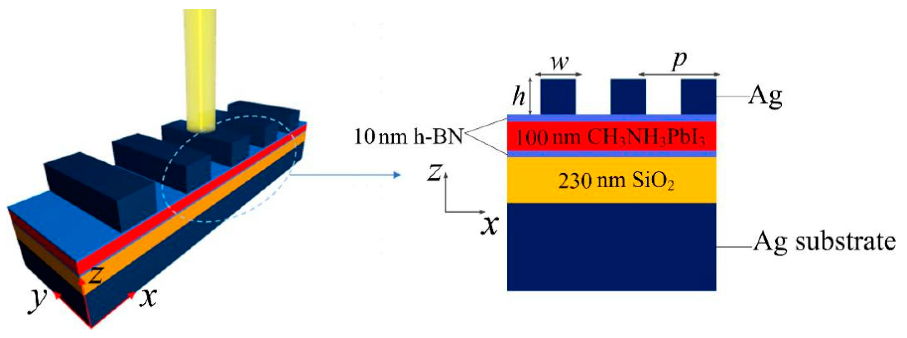
2. Structure Design
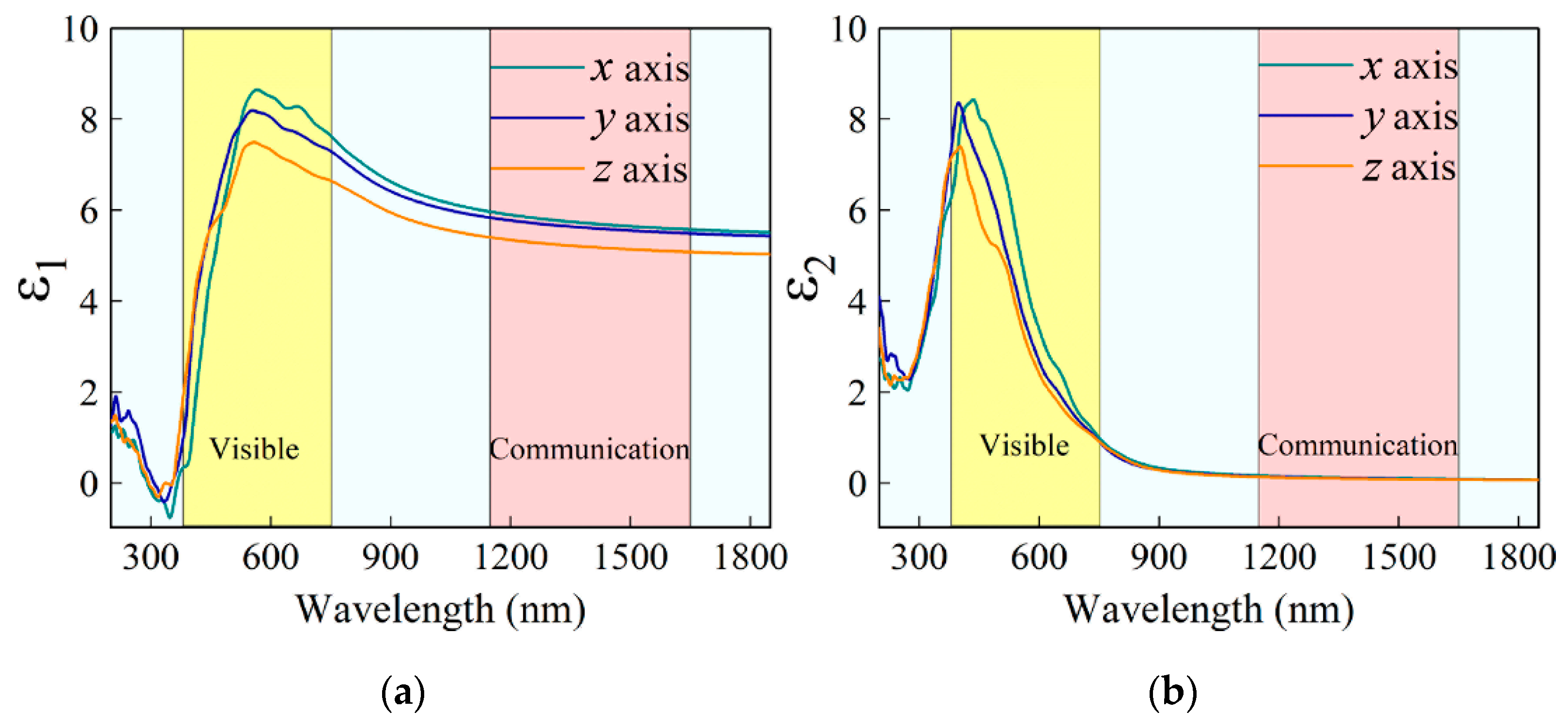
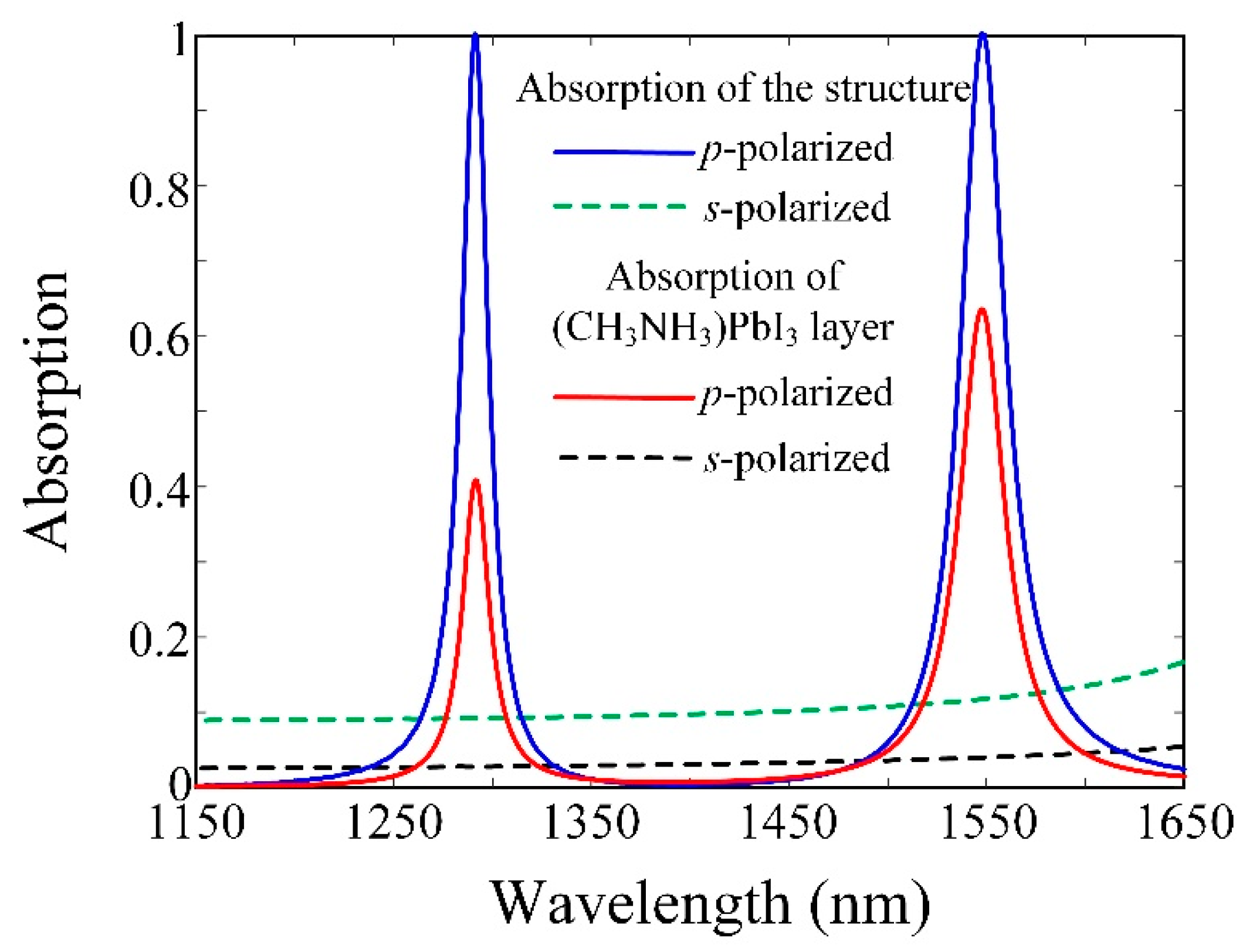
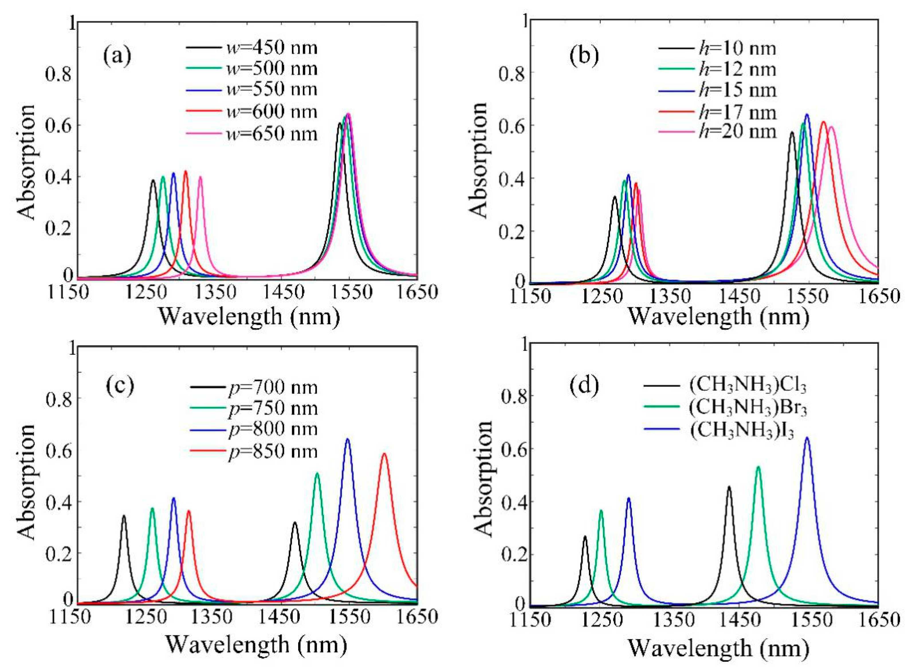
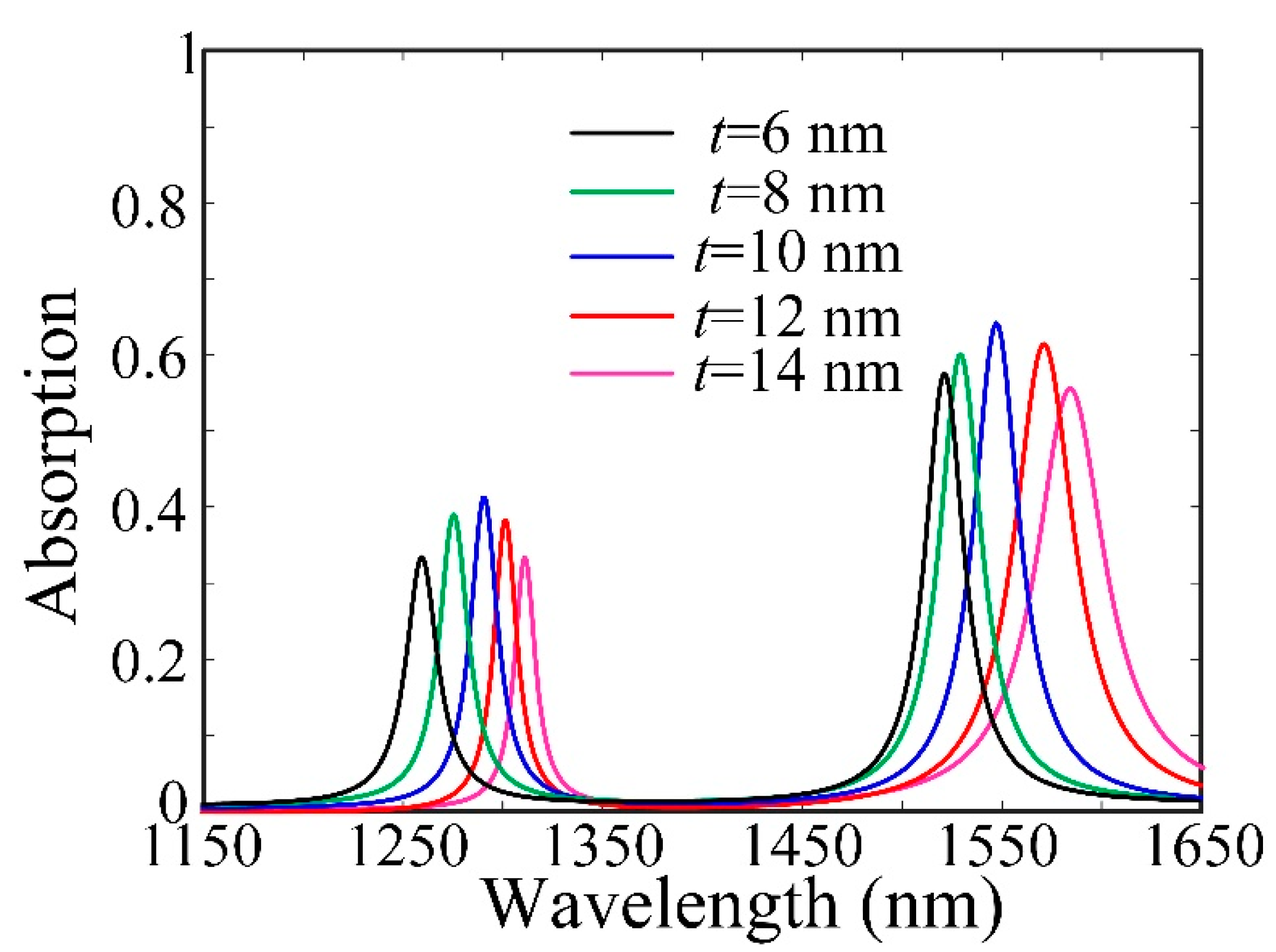
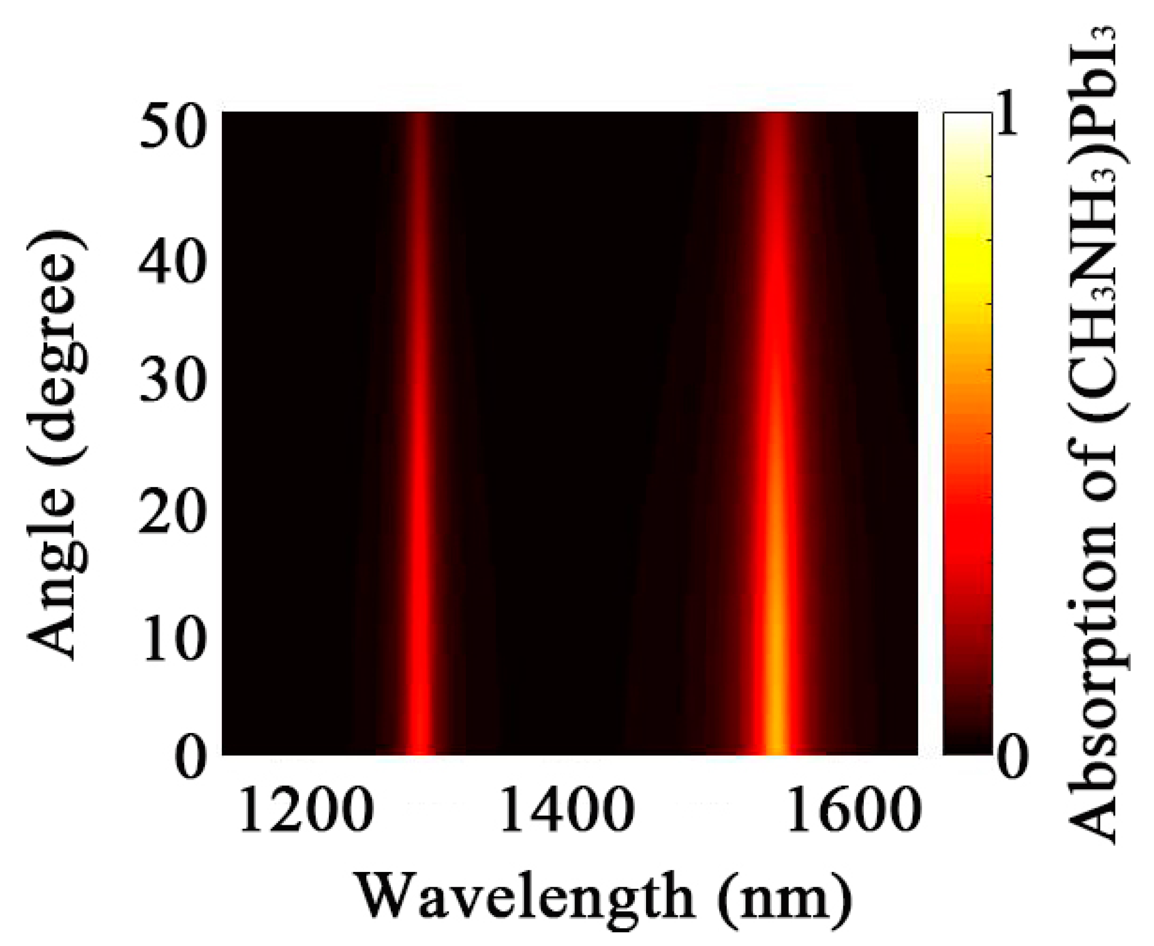
3. Results and Discussion
4. Conclusions
Author Contributions
Funding
Data Availability Statement
Acknowledgments
Conflicts of Interest
References
- Geim, K.; Grigorieva, I.V. Van der Waals heterostructures. Nature 2013, 499, 419. [Google Scholar] [CrossRef] [PubMed]
- Cheng, Z.Q.; Li, Z.L.; Luo, X.; Shi, H.Q.; Luo, C.L.; Liu, Z.M.; Nan, F. Enhanced second harmonic generation by double plasmon resonances in mesoscale flower-like silver particles. Appl. Phys. Lett. 2019, 114, 011901. [Google Scholar] [CrossRef]
- Chen, K.; Adato, R.; Altug, H. Dual-band perfect absorber for multispectral plasmon-enhanced infrared spectroscopy. ACS Nano 2012, 6, 7998–8006. [Google Scholar] [CrossRef]
- Wang, Y.Y.; Chen, Z.Q.; Xu, D.Y.; Yi, Z.; Chen, X.F.; Chen, J.; Tang, Y.J.; Wu, P.H.; Li, G.F.; Yi, Y.G. Triple-band perfect metamaterial absorber with good operating angle polarization tolerance based on split ring arrays. Results Phys. 2020, 16, 102951. [Google Scholar] [CrossRef]
- Luo, X.; Liu, Z.M.; Cheng, Z.Q.; Liu, J.P.; Lin, Q.; Wang, L.L. Polarization-insensitive and wide-angle broadband absorption enhancement of molybdenum disulfide in the visible regime. Opt. Express 2018, 26, 33918. [Google Scholar] [CrossRef] [PubMed]
- Xu, L.; Huang, W.Q.; Hu, W.Y.; Yang, K.; Zhou, B.X.; Pan, A.L.; Huang, G.F. Two-dimensional MoS2-graphene-based multilayer van der Waals heterostructures: Enhanced charge transfer and optical absorption, and electric-field tunable Dirac point and band Gap. Chem. Mater. 2017, 29, 5504. [Google Scholar] [CrossRef]
- Li, J.K.; Chen, Z.Q.; Yang, H.; Yi, Z.; Chen, X.F.; Yao, W.T.; Duan, T.; Wu, P.H.; Li, G.F.; Yi, Y.G. Tunable broadband solar energy absorber based on monolayer transition metal dichalcogenides materials using au nanocubes. Nanomaterials 2020, 10, 257. [Google Scholar] [CrossRef] [PubMed]
- Xia, S.X.; Zhai, X.; Wang, L.L.; Wen, S.C. Plasmonically induced transparency in in-plane isotropic and anisotropic 2D materials. Opt. Express 2020, 28, 7980. [Google Scholar] [CrossRef]
- Luo, X.; Cheng, Z.Q.; Zhai, X.; Liu, Z.M.; Li, S.Q.; Liu, J.P.; Wang, L.L.; Lin, Q.; Zhou, Y.H. A tunable dual-band and polarization-insensitive coherent perfect absorber based on double-layers graphene hybrid waveguide. Nanoscale Res. Lett. 2019, 14, 337. [Google Scholar] [CrossRef]
- Xiao, S.; Wang, T.; Liu, T.; Zhou, C.; Jiang, X.; Zhang, J. Active metamaterials and metadevices: A review. J. Phys. D Appl. Phys. 2020, 53, 503002. [Google Scholar] [CrossRef]
- Xu, L.; Peng, B.J.; Luo, X.; Zhai, X.; Wang, L.L. A broadband and polarization-insensitive perfect absorber based on a van der Waals material in the mid-infrared regime. Results Phys. 2019, 15, 102687. [Google Scholar] [CrossRef]
- Li, Q.; Xu, L.; Luo, K.W.; Li, X.F.; Huang, W.Q.; Wang, L.L.; Yu, Y.B. Electric-field-induced widely tunable direct and indirect band gaps in hBN/MoS2 van der Waals heterostructures. J. Mater. Chem. C 2017, 5, 4426. [Google Scholar] [CrossRef]
- Lu, H.; Gong, Y.K.; Mao, D.; Gan, X.T.; Zhao, J.L. Strong plasmonic confinement and optical force in phosphorene pairs. Opt. Express 2017, 25, 5255. [Google Scholar] [CrossRef] [PubMed]
- Cai, Y.J.; Xu, K.D.; Feng, N.X.; Guo, R.R.; Lin, H.J.; Zhu, J.F. Anisotropic infrared plasmonic broadband absorber based on graphene-black phosphorus multilayers. Opt. Express 2019, 27, 3101. [Google Scholar] [CrossRef] [PubMed]
- Sutherland, R.; Sargent, E.H. Perovskite photonic sources. Nat. Photonics 2016, 10, 295. [Google Scholar] [CrossRef]
- Chen, S.T.; Roh, K.D.; Lee, J.H.; Chong, W.K.; Lu, Y.; Mathews, N.; Nurmikko, T.C.S.A. A photonic crystal laser from solution based organo-lead iodide perovskite thin films. ACS Nano 2016, 6, 3959. [Google Scholar] [CrossRef]
- Zhou, H.; Dong, X.; Jiang, M.M.; Zheng, W.H.; Sun, L.X.; Zhao, B.B.; Tang, B.; Pan, A.L.; Zhang, L. Single-mode lasing and 3D confinement from perovskite micro-cubic cavity. J. Mater. Chem. C 2018, 6, 11740. [Google Scholar] [CrossRef]
- Green, M.A.; Ho-Baillie, A.; Snaith, H.J. The emergence of perovskite solar cells. Nat. Photonics 2014, 8, 506. [Google Scholar] [CrossRef]
- Makarov, S.; Furasova, A.; Tiguntseva, E.; Hemmetter, A.; Berestennikov, A.; Pushkarev, A.; Zakhidov, A.; Kivshar, Y. Halide-perovskite resonant nanophotonics. Adv. Opt. Mater. 2019, 7, 1800784. [Google Scholar] [CrossRef]
- Stranks, S.D.; Eperon, G.E.; Grancini, G.; Menelaou, C.; Alcocer, M.J.P.; Leijtens, T.; Herz, L.M.; Petrozza, A.; Snaith, H.J. Electron-hole diffusion lengths exceeding 1 micrometer in an organometal trihalide perovskite absorber. Science 2013, 342, 341. [Google Scholar] [CrossRef]
- Dong, Q.; Fang, Y.; Shao, Y.; Mulligan, P.; Qiu, J.; Cao, L.; Huang, J. Solar cells. Electron-hole diffusion lengths >175 μm in solution-grown CH3NH3PbI3 single crystals. Science 2015, 347, 967. [Google Scholar] [CrossRef] [PubMed]
- Manser, J.S.; Christians, J.A.; Kamat, P.V. Intriguing optoelectronic properties of metal Halide Perovskites. Chem. Rev. 2016, 116, 12956. [Google Scholar] [CrossRef] [PubMed]
- Kojima, A.; Teshima, K.; Shirai, Y.; Miyasaka, T. Organometal Halide Perovskites as visible-light sensitizers for photovoltaic cells. J. Am. Chem. Soc. 2009, 131, 6050. [Google Scholar] [CrossRef] [PubMed]
- Kim, H.S.; Lee, C.R.; Im, J.H.; Lee, K.B.; Moehl, T.; Marchioro, A.; Moon, S.J.; Baker, R.H.; Yum, J.H.; Moser, J.E.; et al. Lead Iodide Perovskite sensitized all-solid-state submicron thin film mesoscopic solar cell with efficiency exceeding 9%. Sci. Rep. 2012, 2, 591. [Google Scholar] [CrossRef] [PubMed]
- Ball, J.M.; Lee, M.M.; Hey, A.; Snaith, H.J. Low-temperature processed meso-superstructured to thin-film perovskite solar cells. Energy Environ. Sci. 2013, 6, 1739. [Google Scholar] [CrossRef]
- Zhou, H.; Chen, Q.; Li, G.; Li, G.; Luo, S.; Song, T.B.; Duan, H.S.; Hong, Z.R.; You, J.B.; Liu, Y.S.; et al. Interface engineering of highly efficient perovskite solar cells. Science 2014, 345, 542. [Google Scholar] [CrossRef]
- Correa-Baena, J.P.; Abate, A.; Saliba, M.; Tress, W.; Jacobsson, T.J.; Gratzel, M.; Hagfeldt, A. The rapid evolution of highly efficient perovskite solar cells. Energy Environ. Sci. 2017, 10, 710. [Google Scholar] [CrossRef]
- Zhang, Y.P.; Lim, C.K.; Dai, Z.; Yu, G.; Haus, J.W.; Zhang, H.; Prasad, P.N. Photonics and optoelectronics using nano-structured hybrid perovskite media and their optical cavities. Phy. Rep. 2019, 795, 1. [Google Scholar] [CrossRef]
- Hao, J.; Zhou, L.; Qi, M. Nearly total absorption of light and heat generation by plasmonic metamaterials. Phys. Rev. B 2011, 83, 165107. [Google Scholar] [CrossRef]
- Moreau, A.; Ciraci, C.; Mock, J.; Hill, R.; Wang, Q.; Wiley, B.; Chilkoti, A.; Smith, D.R. Controlled-reflectance surfaces with film-coupled colloidal nanoantennas. Nature 2012, 492, 86. [Google Scholar] [CrossRef]
- Johnson, P.B.; Christy, R.W. Optical constants of the noble metals. Phys. Rev. B 1972, 6, 4370. [Google Scholar] [CrossRef]
- Ishii, T.; Sato, T. Growth of single crystals of hexagonal boron nitride. J. Cryst. Growth 1983, 61, 689. [Google Scholar] [CrossRef]
- Jackson, J.D. Classical Electrodynamics, 3rd ed; Wiley: Hobokennm, NJ, USA, 1999. [Google Scholar]
- Kresse, G.; Hafner, J. Ab initio molecular dynamics for liquid metals. Phys. Rev. B 1993, 47, 558. [Google Scholar] [CrossRef] [PubMed]
- Kresse, G.; Furthmuller, J. Efficient iterative schemes for ab initio total-energy calculations using a plane-wave basis set. Phys. Rev. B 1996, 54, 11169. [Google Scholar] [CrossRef]
- Grimme, S. Semiempirical GGA-type density functional constructed with a long-range dispersion correction. J. Comput. Chem. 2006, 27, 1787. [Google Scholar] [CrossRef]
- Shirayama, M.; Kadowaki, H.; Miyadera, T.; Sugita, T.; Tamakoshi, M.; Kato, M.; Fujiseki, T.; Murata, D.; Hara, S.; Murakami, T.N.; et al. Optical transitions in hybrid perovskite solar cells: Ellipsometry, density functional theory, and quantum efficiency analyses for CH3NH3PbI3. Phys. Rev. A 2016, 5, 014012. [Google Scholar] [CrossRef]


Publisher’s Note: MDPI stays neutral with regard to jurisdictional claims in published maps and institutional affiliations. |
© 2021 by the authors. Licensee MDPI, Basel, Switzerland. This article is an open access article distributed under the terms and conditions of the Creative Commons Attribution (CC BY) license (http://creativecommons.org/licenses/by/4.0/).
Share and Cite
Xu, L.; Zeng, J.; Luo, X.; Xia, L.; Ma, Z.; Peng, B.; Li, Z.; Zhai, X.; Wang, L. Dual-Band Plasmonic Perfect Absorber Based on the Hybrid Halide Perovskite in the Communication Regime. Coatings 2021, 11, 67. https://doi.org/10.3390/coatings11010067
Xu L, Zeng J, Luo X, Xia L, Ma Z, Peng B, Li Z, Zhai X, Wang L. Dual-Band Plasmonic Perfect Absorber Based on the Hybrid Halide Perovskite in the Communication Regime. Coatings. 2021; 11(1):67. https://doi.org/10.3390/coatings11010067
Chicago/Turabian StyleXu, Liang, Jian Zeng, Xin Luo, Libin Xia, Zongle Ma, Bojun Peng, Zhengquan Li, Xiang Zhai, and Lingling Wang. 2021. "Dual-Band Plasmonic Perfect Absorber Based on the Hybrid Halide Perovskite in the Communication Regime" Coatings 11, no. 1: 67. https://doi.org/10.3390/coatings11010067
APA StyleXu, L., Zeng, J., Luo, X., Xia, L., Ma, Z., Peng, B., Li, Z., Zhai, X., & Wang, L. (2021). Dual-Band Plasmonic Perfect Absorber Based on the Hybrid Halide Perovskite in the Communication Regime. Coatings, 11(1), 67. https://doi.org/10.3390/coatings11010067