Article

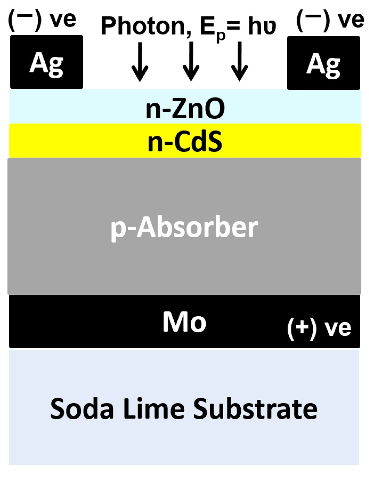
Numerical Insights into the Influence of Electrical Properties of n-CdS Buffer Layer on the Performance of SLG/Mo/p-Absorber/n-CdS/n-ZnO/Ag Configured Thin Film Photovoltaic Devices

by
Asmaa Soheil Najm
1,
Puvaneswaran Chelvanathan
2,3,*,
Sieh Kiong Tiong
4,
Mohammad Tanvirul Ferdaous
5,
Seyed Ahmad Shahahmadi
4,
Yulisa Yusoff
4,
Kamaruzzaman Sopian
2 and
Nowshad Amin
1,4,*
1
Department of Electrical, Electronics and System, FKAB, Universiti Kebangsaan Malaysia (UKM), Bangi 43600, Selangor, Malaysia
2
Solar Energy Research Institute (SERI), Universiti Kebangsaan Malaysia (UKM), Bangi 43600, Selangor, Malaysia
3
Graphene & Advanced 2D Materials Research Group (GAMRG), School of Science and Technology (SST), Sunway University, No. 5, Jalan Universiti, Bandar Sunway 47500, Selangor, Malaysia
4
Institute of Sustainable Energy, Universiti Tenaga Nasional (@The National Energy University), Jalan IKRAM-UNITEN, Kajang 43000, Selangor, Malaysia
5
UNITEN R&D Sdn Bhd, Universiti Tenaga Nasional (@The National Energy University), Jalan IKRAM-UNITEN, Kajang 43000, Selangor, Malaysia
*
Authors to whom correspondence should be addressed.
Coatings 2021, 11(1), 52; https://doi.org/10.3390/coatings11010052
Submission received: 12 November 2020 / Revised: 16 December 2020 / Accepted: 21 December 2020 / Published: 6 January 2021
(This article belongs to the Special Issue Thin Film Dynamics: Theory and Computer Simulations)

Abstract

:
A CdS thin film buffer layer has been widely used as conventional n-type heterojunction partner both in established and emerging thin film photovoltaic devices. In this study, we perform numerical simulation to elucidate the influence of electrical properties of the CdS buffer layer, essentially in terms of carrier mobility and carrier concentration on the performance of SLG/Mo/p-Absorber/n-CdS/n-ZnO/Ag configured thin film photovoltaic devices, by using the Solar Cell Capacitance Simulator (SCAPS-1D). A wide range of p-type absorber layers with a band gap from 0.9 to 1.7 eV and electron affinity from 3.7 to 4.7 eV have been considered in this simulation study. For an ideal absorber layer (no defect), the carrier mobility and carrier concentration of CdS buffer layer do not significantly alter the maximum attainable efficiency. Generally, it was revealed that for an absorber layer with a conduction band offset (CBO) that is more than 0.3 eV, Jsc is strongly dependent on the carrier mobility and carrier concentration of the CdS buffer layer, whereas Voc is predominantly dependent on the back contact barrier height. However, as the bulk defect density of the absorber layer is increased from 1014 to 1018 cm−3, a CdS buffer layer with higher carrier mobility and carrier concentration is an imperative requirement to a yield device with higher conversion efficiency and a larger band gap-CBO window for realization of a functional device. Most tellingly, simulation outcomes from this study reveal that electrical properties of the CdS buffer layer play a decisive role in determining the progress of emerging p-type photo-absorber layer materials, particularly during the embryonic device development stage.

1. Introduction

The conversion of solar energy into usable electricity via a solid-state pn-junction based photovoltaic (PV) device holds immense opportunities in the quest to reduce our present dependence on fossil fuels and subsequently lower the detrimental greenhouse gases emissions [1,2]. Currently, global PV installations are comprised of monocrystalline silicon (c-Si), multicrystalline silicon (mc-Si) and thin film technologies [3]. Thin film photovoltaics can be further divided into 3 successfully commercialized technologies, which are copper indium gallium diselenide (CIGS), cadmium telluride (CdTe) and amorphous silicon (a-Si). Among these, CIGS and CdTe have garnered tremendous interest in the PV research community, which eventually translated into systematic theoretical and experimental studies and consequently achieved a power conversion efficiency (PCE) of more than 22% [4]. However, the scarcity of indium (In) and tellurium (Te) is predicted to hamper the future adoption of CIGS and CdTe at a multi-terawatt level scale [5,6]. Therefore, various earth-abundant, low cost and pure sulfide-based materials such as Cu2ZnSnS4 (CZTS), Cu2SnS3 (CTS), FeS2 and SnS are being rigorously experimented with as for plausible next generation thin film technologies [7,8,9,10,11,12,13,14]. These aforementioned photo-absorber materials are often adopted in the well-established Mo/absorber/CdS/ZnO substrate type device configuration that was developed by ARCO back in 1988, which was one of the key innovations that catalyzed the development of high efficiency CIGS solar cells [15].
Cadmium sulfide (CdS) is an important II–VI compound semiconductor, with high transparency, direct band gap transition (Eg~2.4 eV), high electron affinity (4.2 eV) and n-type conductivity [16,17]. CdS also improves the lattice heterojunction interface match, enhances the excess carrier lifetime and optimizes the band alignment of the devices it is used in [18]. CdS thin film deposition can be done by using various methods, such as magnetron sputtering, chemical vapor transport (CSVT), chemical bath deposition (CBD) and thermal evaporation [19,20,21]. Most of the techniques are very complex and hard to control, and also costly [22]. CBD has been considered as one of the most common fabrication techniques to deposit a buffer layer in solar cells due to its simple deposition process, low costs, high yield and eco-friendliness [23]. Besides, this process can be controlled easily through pH, salt concentration and temperature variations, thereby obtaining a high quality thin film with the desired thickness and crystallinity [7,21]. Different materials with a wider band gap and non-toxic materials such as ZnS (O,OH) and ZnS have also been investigated as a potential buffer layer for thin film solar cells [24,25,26,27].
However, these buffer layers suffer from complicated reaction mechanism and light soaking effects, presenting potential cell durability and reproducibility issues [28]. Knowledge of the optical, electrical and structural characteristics of CdS films is significant in many scientific, technological and industrial applications in the field of optoelectronic devices, especially involving solar cells [23]. Despite comprehensive data on CBD films of CdS in the literature, the optoelectronic properties of these films are not well understood yet. This is because the optoelectrical properties are, to some extent, influenced by the film microstructure, which in turn depends on the preparation and post-deposition conditions. Interestingly, the electrical resistivity of the CdS thin film which essentially depends on the carrier concentration and carrier mobility, has been reported to differ by several orders of magnitude, due not only to the doping level, but also to the film microstructure and thickness [29,30,31] However, systematic studies using numerical simulation on the effects of the carrier mobility and carrier concentration of CdS buffer layer and thus its electrical properties, on the performance of thin film solar cells have not been carried out so far.
Hence, in this study, we have intentionally focused the scope of our numerical simulation by using 1D-SCAPS software to elucidate the interdependence of carrier mobility and carrier concentration of the CdS buffer layer on the PCE of various substrate-type thin film solar cells. A generic substrate-type Soda lime glass (SLG)/Mo/p-absorber/n-CdS/n-ZnO/Ag device configuration has been adopted. In order to maximize the applicability of simulation outcomes, all the possible permutations and combinations of absorber band gap from 0.9 to 1.7 eV and electron affinity from 3.7 to 4.7 eV have been considered. Furthermore, absorber layers with no defect (ideal) and with a peak defect density of 1014 cm−1 (low), 1016 cm−1 (medium) and 1018 cm−1 (high) have also been considered with variations in the carrier mobility and carrier concentration of the CdS buffer layer. The fundamental aim of this study is to accentuate the importance of having a high quality CdS buffer layer (from a electrical property point of view, focusing on high carrier mobility and a high carrier concentration), during the initial development period of a novel photo-absorber material, particularly in substrate-type thin film photovoltaic device configurations that are akin to CIGS technology.

2. Materials and Methods

In this numerical simulation study, SCAPS-1D (version 3.3.07) software has been utilized to simulate the effects of variable carrier mobility and carrier concentration of the CdS buffer layer on the overall performance of substrate-type thin film photovoltaic devices. SCAPS-1D is a one dimensional computer program used to simulate the DC and AC electrical characteristics of thin film heterojunction solar cells, which was developed and constantly updated by a research team led by Marc Burgelman at the University of Gent [32]. The modeling capabilities of SCAPS were specifically designed to mimic the characteristics of CIGS and CdTe thin film solar cells; however, it has also been tested and used for a variety of other cell types. The generic device structure which has been adopted in this study and subsequently modeled in SCAPS is as shown in Figure 1 below. Table 1, Table 2, Table 3 and Table 4 show the list of physical and electronic material properties of all layers, which have been adopted and modeled in the SCAPS simulation tool in the study. A brief literature from the material property perspective for each layers and pertinent theoretical framework is given in the subsequent paragraphs, with the aim to derive a credible justification for the selection of material and hetero-interface electronic parameters which have been used in this study, as shown in Table 1, Table 2, Table 3 and Table 4.
The effects of the SLG substrate on the heterojunction band energy layout was not taken into consideration in the simulation due to the limitations posed by the SCAPS software used in this study. Nonetheless, in reality, diffusion of sodium (Na) from soda lime glass into the absorber layer has been well-documented as one of the adventitious doping mechanisms, which promotes grain growth and elemental interdiffusion and also enhances carrier concentration and defect passivation for several types of photo-absorber materials such as CIGS, CZTS, CTS, FeS2 and SnS [33,34,35,36,37]. Conventionally, in a substrate-type device architecture, molybdenum (Mo) thin film is the primary choice as a back contact due to its chemical inertness, good thermal stability and suitable electrical and optical (reflectivity) properties [38,39]. The work function of the Mo back contact was set to 4.95 eV [40]. Consequently, the majority carrier barrier height at the Mo/absorber interface changed for different values of the band gap and electron affinity of the absorber layer in accordance with Equation (1) below [41]:
Φ Bp = E g Φ Bn
where Eg is the absorber layer band gap and Φ Bn is the minority carrier barrier height, which on the other hand is given by Equation (2) as shown below [40].
Φ Bn = Φ Mo χ s
Φ Mo is the Mo metal work function and χ s is the electron affinity of the absorber layer. Absorber layer thickness was fixed at 2500 nm throughout the entire simulation. The band gap and electron affinity values of the absorber layer were simultaneously varied from 0.9 to 1.7 eV and from 3.7 to 4.7 eV, respectively. Consequently, the corresponding conduction band offset (CBO) (with respect to CdS buffer layer, χ CdS = 4.2   eV ) , ΔEc changed accordingly based on Equation (3), as given below [42]:
Δ E c = χ absorber χ CdS ;   for   n - CdS / p - absorber   heterojunction
where χ absorber and χ CdS are the electron affinity values for the p-absorber layer and n-CdS buffer layer, respectively. With the above-mentioned CBO definition, the following sign convention was established. In a positive CBO ( χ absorber > χ CdS ) or also known as a spike-like CBO, photogenerated electrons have to utilize kinetic energy in order to overcome an energy barrier in the absorber/buffer hetero-interface. Meanwhile in a negative CBO ( χ absorber < χ CdS ) or also termed as a cliff-like CBO, photogenerated electrons gain kinetic energy at this absorber/buffer hetero-interface [43]. This permutation and combination approach has enabled a wide range of performance plot for various known absorber materials, which are currently being experimentally investigated at a lab-scale. A few material systems are identified and tabulated with their band gap, electron affinity and the computed CBO values (with the respect to CdS buffer layer) in Table 5.
Moving on to the central theme of this simulation study, which is the electrical properties of CdS buffer layer, Table 3 shows the 4 different scenarios investigated in this present study. Donor concentration and carrier mobility are varied according to the values given in the Table 4, consequently the electrical resistivity of CdS buffer layer changes according to Equation (4) as described below [52]:
ρ = 1 q μ n N D
where ρ is the resistivity, q is the electron’s charge, while µn and ND is the electron mobility and donor concentration of CdS buffer layer. Basically, the following key features can be deduced from Table 3: Set A and B represents the CdS buffer layer with a lower carrier concentration (1 × 1014 cm−3) and varying electron mobility (set A: 1 cm2/V·s, set B: 100 cm2/V·s). On the other hand, set C and D represents a CdS buffer layer with a higher carrier concentration (1 × 1018 cm−3) and varying electron mobility (set C: 1 cm2/V·s, set D: 100 cm2/V·s). As a result, the CdS buffer layer in set A possesses the highest electrical resistivity of 62,415 Ω·cm, and this value progressively decreases for set B (624.15 Ω·cm) and set C (6.2415 Ω·cm), whereas the CdS buffer layer in set D possesses the lowest electrical resistivity of 0.0624 Ω·cm. Another material property of the absorber layer which was intentionally varied is the defect density. In the first part of this simulation, an ideal absorber layer was assumed, hence the peak defect density of the absorber layer was set to 0 for all cases. In the second part of the simulation, 3 distinct peak defect densities of the absorber layer were assumed; 1 × 10¹⁴, 1 × 10¹⁶ and 1 × 10¹⁸ eV−1·cm−3, respectively. No CdS/absorber interfacial recombination mechanism was implemented in this study. On the other hand, the defect properties of other layers were kept constant. Table 4 summarizes the defect properties for all the relevant layers adopted in this study. The thickness of the CdS buffer layer was kept constant at 50 nm in all cases [53]. A 50 nm thick n-ZnO layer was incorporated as a transparent conducting oxide (TCO) layer on the top CdS buffer layer and was followed by a front contact metal electrode (Ag front electrode). In order to enable ohmic contact between the front electrode and a n-ZnO TCO layer, the work function of the Ag front electrode was set to 4.47 eV. Ag has been reported to possess work functions in the range of 4.26 to 4.74 eV depending on the crystal facet orientation [54]. In other words, a flat-band condition (Φbn = 0) was assumed in the front Ag/n-ZnO metal-semiconductor junction. All numerical simulations were carried out at a constant temperature of 300 K for all cases. No additional series resistance and shunt resistance parameters were defined for simplicity. Built-in standard solar spectrum (AM1.5G-1 Sun) with an integrated power density of 1000 W/m2 was chosen as an illumination bias.
The numerical work presented herein has been carried out in two parts. In the first part, an ideal absorber layer with no defect was assumed and all 4 types of CdS buffer layer (Set A, B, C and D) were considered in the simulation. The outcome and discussion pertaining the first part is delineated in Section 3.2. The second part of this simulation takes into account the absorber layer with its defect density. As mentioned previously, 3 distinct peak defect densities of the absorber layer were assumed, which are 1 × 10¹⁴ eV−1·cm−3 (low), 1 × 10¹⁶ eV−1·cm−3 (medium) and 1 × 10¹⁸ eV−1·cm−3 (high). In the second part, only the CdS buffer layers represented in set A and set D, which corresponds to buffer layers with the lowest and highest resistivity, respectively, were considered. The outcome and discussion pertaining the second part is described in Section 3.3.

3. Results and Discussion

3.1. Interfacial Electronic Parameters of Mo/p-Absorber/n-CdS Heterostructure

Although the primary focus of this study was aimed at elucidating the effects of the electrical properties of the CdS buffer layer on the performance of a thin film photovoltaic device, one aspect of this simulation study that must be explicated prior to delving into the aforementioned scope is the back contact barrier height (ΦBp). This is due to the fact that the back contact barrier height, which is an important interfacial electronic parameter at the Mo/p-absorber metal-semiconductor interface changes with the band gap and electron affinity of the p-absorber layer, as described in Equations (1) and (2). Figure 2 below depicts the resulting back contact barrier height as a function of the band gap and electron affinity of the absorber layer.
The top x-axis represents the CBO values for the corresponding electron affinity of the absorber layer given in the bottom x-axis, which is in accordance with Equation (3). Negative and zero back contact barrier height denotes ohmic contact between Mo and the p-absorber layer, while a positive value represents a rectifying contact. In an optimal photovoltaic device, ohmic contact is preferred, which is defined as contact that allows unimpeded flow of the hole through diffusion from the valence band of the p-absorber layer into the partially filled band of metal. An ohmic metal-semiconductor contact generally exhibits linear current–voltage characteristics in both biasing directions (−V to +V) [55]. On the other hand, a rectifying contact or also known as a Schottky contact is less favorable due to the existence of a potential barrier which retards the hole diffusion from the p-absorber into the back contact metal. Therefore, referring to Figure 2, it can be deduced that an absorber layer with an electron affinity of 3.7 to 4.0 eV and a band gap of 0.9 to 1.2 eV (bottom-left corner of the plot), forms an ohmic contact with the Mo back contact. Concomitantly, the absorber layer within this range forms a cliff-like CBO of −0.50 to −0.20 eV with the CdS buffer layer. Meanwhile, the rest of the potential absorber material which fall outside the aforementioned electron affinity and band gap region was projected to form a Schottky contact with Mo metal.
There are 2 essential characteristics pertaining to the resulting back contact barrier height values, which have significant impacts on the applicability of this simulation work. Firstly, in this simulation, no interfacial layer between the Mo back contact and p-absorber layer was assumed, hence Figure 2 represents the theoretical values of a back contact barrier height. In reality, interaction of chalcogen atoms such as S and Se with Mo back contact during layer deposition and heat treatment is known to induce an unintentional interfacial layer [56,57]. This interfacial layer substantially alters the charge transport at the Mo/p-absorber interface. For instance, in theory, a CIGSe absorber layer is supposed to form a Schottky contact with Mo due to its large work function; however, the formation of an advantageous p-MoSe2 interfacial layer warrants ohmic contact and subsequently promotes photogenerated charge collection at the back contact region [58,59]. On the other hand, in CZTS based devices, a n-MoS2 interfacial layer has been recognized as a detrimental component which is responsible for higher series resistance, thus leading to lower conversion efficiency [60,61]. The central reason for not including an interfacial layer in this simulation approach is essentially due to the non-specificity of absorber layer material, thus rendering any inclusion interfacial layer to be speculative in nature. Secondly, we were well aware that by masking the effects of back contact barrier height with a flat-band option (ΦBp = 0) for the entire range of the absorber layer, this in turn, affects the electrical properties of the CdS buffer layers on the performance of the thin film photovoltaic device, which the central and intended theme of this study suggests could be greatly augmented. However, we consciously chose not to exercise this option with the aim to preserve the relevance of the simulation outcome with regards to the adoption of Mo as the back contact in the SLG/Mo/p-absorber/n-CdS/n-ZnO/Ag device configuration. The significance of the back contact barrier height and its influence on the photovoltaic performance parameters will be highlighted in the subsequent section whenever the need arises.

3.2. Case I: Ideal Absorber Layer (No Defect)

Figure 3 below depicts the effects of carrier mobility and carrier concentration of the CdS buffer layer on the efficiency of a thin film solar cell with an ideal absorber layer.
By comparing Figure 3a–c and Figure 3b–d, it can be clearly seen that for a constant carrier mobility, a CdS buffer layer with higher carrier concentrations results in a minor increase in the conversion efficiency. By scrutinizing Figure 3 as well, a couple of similar patterns were observed and highlighted as follows. Firstly, regardless of the electrical properties of the CdS buffer layer, an absorber layer with lowest band gap of 0.9 eV and CBO of −0.5 eV produces the thin film solar cell with the highest efficiency in the 30% range. Secondly, the lowest performing devices are generally composed of an absorber layer with CBO in the range of 0.3 to 0.5 eV. On the other hand, a couple of conspicuous distinctions were observed on the conversion efficiency pattern with respect to the different electrical properties of the CdS buffer layer, namely affecting the carrier mobility. Firstly, it could be clearly seen that as the carrier mobility increases from 1 to 100 cm2/V·s irrespective of carrier concentration, the low efficiency window (<5%) shrinks considerably. Concurrently, an efficiency of more than 20% which was initially centered at a band gap of 1.4 eV and CBO of −0.25 eV expands to a larger region, which is indicative of the wider suitability of the CdS buffer layer for a broader range of photo-absorber materials.
We attempt to delineate the observed trend as depicted in Figure 3 by dissecting the relevant photovoltaic performance parameters, which ultimately govern the solar cell conversion efficiency. Generally, the conversion efficiency is calculated according to Equation (5) as shown below, whereby FF is the fill factor, Voc is open circuit voltage, Jsc is short circuit current and Pin is input power [62].
Ƞ = F F   V o c   J s c P i n
For the purpose of clarity and simplicity, simulation outcomes pertaining to the CdS buffer layer of set A and set D, which represents the lower and upper limit in terms of carrier mobility and carrier concentration values, were chosen for comparative analysis. Figure 4 and Figure 5 illustrate the (a) Voc, (b) Jsc, (c) FF and (d) η for a thin film photovoltaic device with a CdS buffer layer of set A and set D, respectively. Corresponding results for the CdS buffer layer of set B and set D are given in supplementary information (SI) as Figures S1 and S2, respectively. It is important to note that absorber layer with negative CBO values yields higher efficiency compared to a absorber layer with a positive CBO. This observed occurrence is contrary to the outcome of practical measurements whereby a small positive CBO in the range of 0.1 to 0.4 eV conventionally results in higher conversion efficiency and a negative CBO is expected to yield lower efficiency [63,64,65,66]. However, these phenomena are not reflected in this study due to the fact that the beneficial effects of a small positive CBO and detrimental effects of a negative CBO only come into play if a n-CdS/p-absorber hetero-interface recombination mechanism is taken into account. Due to the scope of this study, which focuses primarily on the electrical properties of the CdS buffer layer and its suitability for a set of variable absorber layers with different bulk defect densities, interfacial recombination mechanism was not incorporated. The interdependence between CdS electrical properties with an element of an interfacial recombination mechanism and their combined influence on the photovoltaic performance of various thin film solar cells deserves an entirely discrete numerical simulation study. Nonetheless, partial treatments of the suggested study as above, which solely focuses on CIGS solar cells, can be found elsewhere [67,68].
By comparing Figure 4a and Figure 5a, it is can been seen that the Voc parameter registers insignificant changes. In fact, similar Voc plots were also observed for Figures S1a and S2a, indicating there is another variable that dictates the resulting Voc, regardless of the electrical properties of the CdS buffer layer. We postulate that the back contact barrier height between Mo and p-absorber as depicted in Figure 2 in tandem with absorber band gap is accountable for the Voc trend. It has been experimentally proven that when the back contact barrier height approaches a certain threshold value, Voc is severely reduced under the reach through a diode regime [69,70]. From this simulation, we have found that for an absorber layer with a band gap of 0.9 eV, a back contact barrier height of more than 0.55 eV results in the Voc value being pegged at 0.4 V or lower. As the band gap is increased linearly, a back contact barrier height with a similar incremental rate yields a similarly low Voc in the region of 0.3 V to 0.4 eV for the entire investigated range of the absorber band gap. Hence, it can be said that for an ideal absorber layer (no defect), Voc is predominantly influenced by the absorber layer band gap and back contact barrier height, rather than by the electrical properties of the CdS buffer layer. On the other hand, the Jsc parameter differs considerably as illustrated in Figure 4b and Figure 5b, mainly in the high CBO region of > 0.3 eV. CdS with higher electrical resistivity (Set A- Figure 4b) records an abrupt decline in the Jsc onset of an CBO value of 0.35 eV. A positive CBO represents a spike-like band edge, which causes an impediment to the transport of photogenerated carriers (electrons) with a low carrier mobility, and subsequently yields lower carrier collection at the front contact and thus a lower Jsc. However, CdS with a higher carrier mobility and carrier concentration (Set D- Figure 5b) could retain a high Jsc value in the same CBO region. This could be due to the increased diffusivity (Dn) of carriers, induced by higher carrier mobility as governed by the equation shown below [71]:
D n = µ n   k B   T q
where Dn, µn, kB, T and q are the carrier diffusivity, electron mobility, Boltzmann constant, absolute temperature and the magnitude of charge of an electron, respectively. In return, increased diffusivity is responsible for a longer carrier diffusion length and subsequently for a higher photogenerated current, Iph as evident in the following relationship shown in Equations (7) and (8) below [61]:
L n = D n τ n
I p h = q A G ( L n + W + L p )
where Ln/p is the diffusion length of the electron/hole, Dn is the carrier diffusivity and τn is the carrier lifetime, meanwhile A is the cross-sectional area, G is the carrier generation rate and W is the depletion width of the heterojunction. Based on Equation (9) below, we note that the depletion region width, W for a heterojunction consisting of CdS with a higher carrier concentration (Set D- ND: 1018 cm−3) should be lower compared to the depletion width for CdS with a lower carrier concentration (Set A- ND: 1014 cm−3) [72]:
W d = [ 2 1 2 ( V b i V ) ( N A 2 + N D 2 ) q ( 1 N D + 2 N A ) N D N A ] 1 / 2
where q, ε1, ε2, Vbi, V, NA, and ND are the electric charge of an electron, dielectric permittivity of CdS, dielectric permittivity of p-absorber, built-in voltage, applied voltage, acceptor concentration in the p-absorber layer and donor concentration in a CdS buffer layer, respectively. However, a higher Jsc value for CBO > 0.3 eV was recorded for CdS of Set D (Figure 5b) despite the reduced depletion width, which was supposed to decrease the photogenerated current according to Equation (8). This could be due to beneficial synergistic effects of high carrier mobility and a narrower depletion region, which enables carriers to overcome a high CBO barrier. This is supported by the fact that only CdS of Set D, which represents a buffer layer with the highest carrier mobility and highest carrier concentration, exhibits a high Jsc across all investigated CBO values (please see Figures S1b and S2b in the supplementary data for the Jsc plot for CdS of Set B and Set C, respectively).

3.3. Case II: Absorber Layer with Variable Defect Density

In this section, the performance of thin film solar cells consisting of absorber layer with varying defect density is presented and discussed. Figure 6a–f below shows the conversion efficiency for a thin film device with the variable absorber layer bulk defect density and electrical properties of the CdS buffer layer (the corresponding Voc, Jsc and FF plots for Figure 6 are given in supplementary data as Figures S3–S5, respectively). Again, with the aim to highlight the discernible role of carrier mobility and carrier concentration of the buffer layer, simulation outcomes for CdS of Set A (µ: 1 cm2/V·s and ND: 1014 cm−3) and Set D (µ: 100 cm2/V·s and ND: 1018 cm−3) have been selectively chosen for comparative analysis. Overall, as the defect density increased, efficiency decreased quite dramatically. This was not unexpected due to the fact that defect states act as detrimental recombination centers for photo-generated charge carriers [73]. It is also evident that an increase in the carrier mobility and carrier concentration of the CdS buffer layer yields higher efficiency and more importantly, enables realization of a functional device across a wider range of absorber band gaps and absorber electron affinities. As an example, for an absorber defect density of 1014 cm−3 (Figure 6a,b) and 1016 cm−3 (Figure 6c,d), by increasing the carrier mobility and carrier concentration of the CdS buffer layer, a functional device could be realized at CBO > 0.3 eV. This is due to the same reason as explained in the previous section, which is for the retention of high Jsc due to a higher carrier diffusivity and efficient carrier transport across a spike-like CBO barrier, particularly for CBO > 0.3 eV (Please see Figure S3a–d).
As the absorber defect layer is increased to 1016 and 1018 cm−3, one important finding is the shift of optimal Eg from lower values (0.9 eV), as observed in case of a defect free absorber to higher values (1.4 to 1.5 eV). This is probably due to a comparatively higher impact of defect states in a narrow band gap material than a wider band gap material [74]. This fact is further exemplified in the Voc plot (Please see Figure S4), whereby a decrease in the Voc parameter for the absorber layer with the highest defect density of 1018 cm−3 is unmistakably evident, particularly for an absorber band gap of 0.9 eV, regardless of the CBO value. An increase in the carrier mobility and carrier concentration of the CdS buffer layer shifts the efficiency sweet spot from a CBO of −0.2 to −0.1 and Eg of 1.2 to 1.4 eV to a slightly narrower region ranging from a lower CBO of −0.4 to −0.3 to a higher Eg of 1.45 to 1.6 eV, as depicted in Figure 6e,f.
Based on the results and discussion from the previous sub-sections, significant impacts of electrical properties of the CdS buffer layer on the development of substrate type configured thin film photovoltaic technology are emphasized as follows. A SLG/Mo/p-absorber/n-CdS/n-ZnO/Ag device configuration is conventionally adopted in the initial development of novel and emerging p-type photo-absorber material. The primary reason for this choice is mainly due to its efficacious implementation as a preliminary baseline recipe in CIGS based technology development, which eventually led to successful commercialization at the gigawatt level after various optimizations in material, process and device fabrication levels [75]. As a consequence, deposition of CdS thin film by the CBD method has been extensively studied and subsequently adopted as the preferred buffer layer material in various photovoltaic research laboratories worldwide. From the electrical properties of the CdS buffer layer perspective, high carrier mobility implies a CdS thin film with lesser structural imperfections (grain boundary, dislocation density and point defects), which eventually leads to reduced carrier scattering [76,77]. On the other hand, a high carrier concentration implies the existence of a suitable shallow donor level below the conduction band edge Ec either due to extrinsic doping or intrinsic native defects, which increases the free electron density in the conduction band through the thermal ionization process [71,78]. Therefore, to achieve the desired electrical property, the microstructural properties of CdS thin film and a doping mechanism which are at play need to be meticulously modulated through deposition, doping and post-deposition process optimizations. However, in the initial stage of explorative investigation of an emerging p-absorber thin film material, the central scope and effort are always focused on the absorber layer material development (material synthesis, deposition process, post-deposition treatment and thin film characterization). Due to this skewed focus, the buffer layer deposition process is usually treated as part of the device completion fabrication step, in which a routine CdS-CBD ‘baseline’ recipe is usually being utilized. This ‘baseline’ recipe typically originates from previous in-house optimization, which was used to deposit CdS as a heterojunction partner for different p-absorber material or was adapted from pertinent literature. We argue that if the electrical properties of the ensuing CdS buffer layer are not properly fine-tuned and characterized, it may lead to incorrect assumptions particularly on the true potential of the investigated p-absorber material. For example, let us say that a particular p-absorber material with band gap of 1.1 eV and CBO of 0.1 eV is being investigated. In the preliminary stage of development, it is highly likely for the absorber thin film to possess a high bulk defect density (i.e., 1018 cm−3) due to its polycrystalline nature and non-optimized deposition process. If the deposited CdS buffer layer possesses low carrier mobility and a low carrier concentration, the corresponding device is predicted to yield efficiency below 5% (see Figure 6e). However, the device efficiency can be boosted above 5% by employing a CdS buffer layer with a higher carrier mobility and higher carrier concentration (see Figure 6f). Although the difference in conversion efficiency seems to be inconspicuously small, nevertheless the initial device performance of a new p-absorber material plays a paramount role in determining its subsequent progression trajectory, through further systematic and sustained investigation. Therefore, there exists a substantial possibility for an emerging absorber material to be prematurely dismissed as a promising photovoltaic material, merely after a few experimental attempts, partially due to non-optimal electrical properties of its CdS buffer layer.
We also note that the electrical properties of CdS thin films, namely the carrier mobility, carrier concentration and resistivity which are reported across the present literature, are predominantly characterized by a ‘dark’ Hall measurement. At the same time, the photoconductivity phenomenon in CdS thin film has been well-documented [79]. Since the basis of thin film solar cell operation is converting light into electricity, understanding the complete charge carrier dynamics of a CdS buffer layer under illumination could be the key to unlocking pathways towards high efficiency thin film solar cells. With the recent advent of the carrier-resolved photo-Hall effect technique, which permits simultaneous measurement of mobility and concentration of both majority and minority carriers, as well as the recombination lifetime, diffusion length and recombination coefficient, we believe this method will shed more insights into the electrical properties of the CdS buffer layer in the near future [80].

4. Conclusions

The numerical simulation works presented herein are primarily focused on assessing the impacts of the electrical properties of the CdS buffer layer, namely the carrier mobility and carrier concentration on the performance of SLG/Mo/p-Absorber/n-CdS/n-ZnO/Ag configured thin film photovoltaic devices. For an ideal absorber layer (no defect), the carrier mobility and carrier concentration of the CdS buffer layer do not significantly alter the maximum attainable efficiency. Generally, it was revealed that Jsc is strongly dependent on the carrier mobility and carrier concentration of the CdS buffer layer for absorber layer with a CBO of more than 0.3 eV, whereas Voc is predominantly dependent on the back contact barrier height. In an ideal case (p-absorber layer with no defect), the highest conversion efficiency is achieved and it was found that the electrical properties of CdS have a less significant impact on the conversion efficiency. Generally, the conversion efficiency is reduced as the bulk defects are introduced in the absorber layer. However, as the bulk defect density of the absorber layer is increased from 1014 to 1018 cm−3, the CdS buffer layer with a higher carrier mobility and carrier concentration yielded devices with a higher conversion efficiency and most importantly, a larger band gap-CBO window for the realization of functional devices. These observed outcomes were attributed to beneficial synergistic effects of high carrier mobility and a narrower depletion region, which enable carriers to overcome a high CBO barrier. By inference, we have also highlighted that a CdS buffer layer with a high carrier mobility and carrier concentration is an indispensable component in the development of any particular substrate type thin film photovoltaic technology.

Supplementary Materials

The following are available online at https://www.mdpi.com/2079-6412/11/1/52/s1, Figure S1: Photovoltaic performance parameters for an ideal p-absorber layer with a CdS buffer layer of Set B (µ: 100 cm2/V·s and ND: 1014 cm−3); Figure S2: Photovoltaic performance parameters for an ideal p-absorber layer with a CdS buffer layer of Set D (µ: 1 cm2/V·s and ND: 1018 cm−3); Figure S3: Effects of µ and ND of a CdS buffer layer on the open circuit voltage of thin film solar cell with a practical p-absorber layers having a different bulk defect density (BDD); Figure S4: Effect of µ and ND of a CdS buffer layer on the short circuit current density of a thin film solar cell with a practical p-absorber layer having a different bulk defect density (BDD); Figure S5: Effect of µ and ND of a CdS buffer layer on the fill factor of thin film solar cell with a practical p-absorber layer having a different bulk defect density (BDD).

Author Contributions

Conceptualization, P.C.; methodology, A.S.N., P.C., M.T.F., S.A.S. and N.A.; software, A.S.N. and P.C.; validation, A.S.N., P.C., M.T.F., S.A.S. and Y.Y.; formal analysis, A.S.N., P.C., M.T.F. and S.A.S.; resources, P.C., S.K.T., N.A. and K.S.; data curation, A.S.N., P.C., M.T.F., S.A.S. and Y.Y.; writing—original draft preparation, A.S.N., P.C., M.T.F. and S.A.S.; writing—review and editing, A.S.N., P.C., M.T.F., S.A.S. and Y.Y.; visualization, P.C., M.T.F., S.A.S. and N.A.; supervision, P.C., K.S. and N.A.; project administration, P.C., S.K.T., N.A. and K.S.; funding acquisition, P.C., S.K.T., K.S. and N.A. All authors have read and agreed to the published version of the manuscript.

Funding

This research was funded by Universiti Kebangsaan Malaysia (UKM), research grant number GP-2020-K022786. The publication of this work was supported by UNITEN through its Internal Research Grant Opex (RJO10517919/iRMC/Publication).

Data Availability Statement

Data sharing is not applicable to this article.

Acknowledgments

The SCAPS (3.3.07) simulation software used in this study was provided by Marc Burgelman, University of Gent, Belgium.

Conflicts of Interest

The authors declare that no conflict of interest exists involving any parties. The funders had no role in the design of the study; in the collection, analyses, or interpretation of data; in the writing of the manuscript, or in the decision to publish the results.

References

  1. Zhuk, S.; Kushwaha, A.; Wong, T.K.S.; Masudy-Panah, S. Critical review on sputter-deposited Cu2ZnSnS4 (CZTS) based thin fi lm photovoltaic technology focusing on device architecture and absorber quality on the solar cells performance. Sol. Energy Mater. Sol. Cells 2016, 171, 239–252. [Google Scholar] [CrossRef]
  2. Najm, A.S.; Ludin, N.A.; Abdullah, M.F.; Almessiere, M.A.; Ahmed, N.M.; Al-Alwani, M.A.M. Areca catechu extracted natural new sensitizer for dye-sensitized solar cell: Performance evaluation. J. Mater. Sci. Mater. Electron. 2020, 31, 3564–3575. [Google Scholar] [CrossRef]
  3. Nayak, P.K.; Mahesh, S.; Snaith, H.J.; Cahen, D. Photovoltaic solar cell technologies: Analysing the state of the art. Nat. Rev. Mater. 2019, 4, 269–285. [Google Scholar] [CrossRef]
  4. Green, M.; Dunlop, E.; Hohl-Ebinger, J.; Yoshita, M.; Kopidakis, N.; Hao, X. Solar cell efficiency tables (version 57). Prog. Photovolt. Res. Appl. 2020, 27, 3–12. [Google Scholar] [CrossRef] [Green Version]
  5. Candelise, C.; Winskel, M.; Gross, R. Implications for CdTe and CIGS technologies production costs of indium and tellurium scarcity. Prog. Photovolt. Res. Appl. 2012, 20, 816–831. [Google Scholar] [CrossRef]
  6. Grandell, L.; Höök, M. Assessing rare metal availability challenges for solar energy technologies. Sustainability 2015, 7, 11818–11837. [Google Scholar] [CrossRef] [Green Version]
  7. Yan, C.; Huang, J.; Sun, K.; Johnston, S.; Zhang, Y.; Sun, H.; Pu, A.; He, M.; Liu, F.; Eder, K.; et al. Cu2ZnSnS4 solar cells with over 10% power conversion efficiency enabled by heterojunction heat treatment. Nat. Energy 2018, 3, 764–772. [Google Scholar] [CrossRef]
  8. Ferdaous, M.; Chelvanathan, P.; Shahahmadi, S.; Sapeli, M.; Sopian, K.; Amin, N. Compositional disparity in Cu2ZnSnS4 (CZTS) thin film deposited by RF-sputtering from a single quaternary compound target. Mater. Lett. 2018, 221, 201–205. [Google Scholar] [CrossRef]
  9. Umehara, M.; Takeda, Y.; Motohiro, T.; Sakai, T.; Awano, H.; Maekawa, R. Cu2Sn1−xGexS3(x = 0.17) thin-film solar cells with high conversion efficiency of 6.0%. Appl. Phys. Express 2013, 6, 045501. [Google Scholar] [CrossRef]
  10. Sabbir, E.; Chelvanathan, P.; Ahmad, S.; Bais, B.; Kiong, S.; Sopian, K. Fabrication of Cu2SnS3 thin film solar cells by sulphurization of sequentially sputtered Sn/CuSn metallic stacked precursors. Sol. Energy 2019, 177, 262–273. [Google Scholar]
  11. Prabukanthan, P.; Thamaraiselvi, S.; Harichandran, G. Single step electrochemical deposition of p-type undoped and Co2+Doped FeS2 thin films and performance in heterojunction solid solar cells. J. Electrochem. Soc. 2017, 164, D581–D589. [Google Scholar] [CrossRef]
  12. Shukla, S.; Xing, G.; Ge, H.; Prabhakar, R.R.; Mathew, S.; Su, Z.; Nalla, V.; Venkatesan, T.; Mathews, N.; Sritharan, T.; et al. Origin of photocarrier losses in iron pyrite (FeS2) nanocubes. ACS Nano 2016, 10, 4431–4440. [Google Scholar] [CrossRef] [PubMed]
  13. Sinsermsuksakul, P.; Sun, L.; Lee, S.W.; Park, H.H.; Kim, S.B.; Yang, C.; Gordon, R.G. Overcoming efficiency limitations of SnS-based solar cells. Mater. Views 2014, 15, 1400496. [Google Scholar] [CrossRef]
  14. Spalatu, N.; Hiie, J.; Kaupmees, R.; Volobujeva, O.; Krustok, J.; Acik, I.O.; Krunks, M. Postdeposition processing of SnS thin films and solar cells: Prospective strategy to obtain large, sintered, and doped SnS grains by recrystallization in the presence of a metal halide flux. ACS Appl. Mater. Interfaces 2019, 11, 17539–17554. [Google Scholar] [CrossRef]
  15. Mitchell, K.; Potter, R.; Ermer, J.; Wieting, R.; Eberspacher, C. High efficiency thin film tandem PV modules. In Proceedings of the 19th IEEE Hotovoltaic Specialists Conference, New Orleans, LA, USA, 4–8 May 1987; pp. 13–18. [Google Scholar]
  16. Holi, A.M.; Al-Zahrani, A.A.; Najm, A.S.; Chelvanathan, P.; Amin, N. PbS/CdS/ZnO nanowire arrays: Synthesis, structural, optical, electrical, and photoelectrochemical properties. Chem. Phys. Lett. 2020, 750, 137486. [Google Scholar] [CrossRef]
  17. Najm, A.S.; Chowdhury, M.S.; Munna, M.T.; Chelvanathan, P.; Selvanathan, V.; Aminuzzaman, M.; Techato, K.; Amin, N.; Akhtaruzzaman, M.D. Impact of cadmium salt concentration on Cds nanoparticles synthesized by chemical precipitation methot. Chalcogenide Lett. 2020, 17, 537–547. [Google Scholar]
  18. Voznyi, A.; Kosyak, V.; Opanasyuk, A.; Tirkusova, N.; Grase, L.; Medvids, A. Structural and electrical properties of SnS2 thin films. Mater. Chem. Phys. 2016, 173, 52–61. [Google Scholar] [CrossRef] [Green Version]
  19. Yusoff, Y.; Chelvanathan, P.; Huda, Q.; Akhtar, P.; Alam, M.M.; Al-Othman, Z.A.; Amin, N. High quality CdS thin film growth by avoiding anomalies in chemical bath deposition for large area thin film solar cell application. J. Nanosci. Nanotechnol. 2015, 15, 9240–9245. [Google Scholar] [CrossRef]
  20. Islam, M.; Hossain, S.; Aliyu, M.; Chelvanathan, P.; Huda, Q.; Karim, M.; Sopian, K.; Amin, N. Comparison of structural and optical properties of CdS thin films grown by CSVT, CBD and sputtering techniques. Energy Procedia 2013, 33, 203–213. [Google Scholar] [CrossRef] [Green Version]
  21. Memarian, N.; Rozati, S.M.; Concina, I.; Vomiero, A. Deposition of nanostructured CdS thin films by thermal evaporation method: Effect of substrate temperature. Materials 2017, 10, 773. [Google Scholar] [CrossRef]
  22. Parvez, S.; Khabir, K.M. Chemical bath deposition of CdS layer for thin film solar cell. South Asian J. Res. Eng. Sci. Technol. 2017, 2, 3. [Google Scholar]
  23. Zheng, X.; Li, W.; Aberle, A.G.; Venkataraj, S. Efficiency enhancement of ultra-thin Cu(In,Ga)Se2 solar cells: Optimizing the absorber bandgap profile by numerical device simulations. Curr. Appl. Phys. 2016, 16, 1334–1341. [Google Scholar] [CrossRef]
  24. Nakada, T.; Mizutani, M. 18% Efficiency Cd-free Cu(In,Ga)Se2 thin-film solar cells fabricated using chemical bath deposition (CBD)—ZnS buffer layers fabricated using chemical bath deposition (CBD)-ZnS buffer layers. Jpn. J. Appl. Phys. 2002, 41, 165. [Google Scholar] [CrossRef]
  25. Chelvanathan, P.; Yusoff, Y.; Haque, F.; Akhtaruzzaman, M.; Alam, M.; Alothman, Z.; Rashid, M.; Sopian, K.; Amin, N. Growth and characterization of RF-sputtered ZnS thin film deposited at various substrate temperatures for photovoltaic application. Appl. Surf. Sci. 2015, 334, 138–144. [Google Scholar] [CrossRef]
  26. Ho, W.-H.; Hsu, C.-H.; Yeh, T.-H.; Chang, Y.-H.; Wei, S.-Y.; Lin, T.-Y.; Lay, C.-H. Room-temperature chemical solution treatment for flexible ZnS(O, OH)/Cu(In,Ga)Se2 solar cell: Improvements in interface properties and. ACS Appl. Mater. Interfaces 2016, 8, 6709–6717. [Google Scholar] [CrossRef] [PubMed]
  27. Benzetta, A.; El, H.; Abderrezek, M.; Elamine, M. Numerical analysis of potential buffer layer for Cu2ZnSnS4 (CZTS) solar cells. Optik Stuttg. 2019, 204, 164155. [Google Scholar]
  28. Slonopas, A.; Ryan, H.; Foley, B.; Sun, Z.; Sun, K.; Globus, T.; Norris, P. Growth mechanisms and their effects on the opto-electrical properties of CdS thin films prepared by chemical bath deposition. Mater. Sci. Semicond. Process. 2016, 52, 24–31. [Google Scholar] [CrossRef]
  29. Khallaf, H.; Chai, G.; Lupan, O.; Chow, L.; Park, S.; Schulte, A. Characterization of gallium-doped CdS thin films grown by chemical bath deposition. Appl. Surf. Sci. 2009, 255, 4129–4134. [Google Scholar] [CrossRef]
  30. Khallaf, H.; Chai, G.; Lupan, O.; Chow, L.; Park, S. Investigation of aluminium and indium in situ doping of chemical bath deposited CdS thin films. J. Phys. D Appl. Phys. 2008, 41, 185304. [Google Scholar] [CrossRef] [Green Version]
  31. Azmi, N.; Chelvanathan, P.; Yusoff, Y.; Shahahmadi, S.; Tiong, S.; Sopian, K.; Amin, N. A comprehensive study on the effects of alternative sulphur precursor on the material properties of chemical bath deposited CdS thin films. Ceram. Int. 2020, 46, 18716–18724. [Google Scholar] [CrossRef]
  32. Burgelman, M.; Nollet, P.; Degrave, S. Modeling polycrystalline semiconductor solar cells. Thin Solid Films 2000, 362, 527–532. [Google Scholar] [CrossRef]
  33. Colombara, D.; Werner, F.; Schwarz, T.; Infante, I.C.; Fleming, Y.; Valle, N.; Spindler, C.; Vacchieri, E.; Rey, G.; Guennou, M.; et al. Sodium enhances indium-gallium interdiffusion in copper indium gallium diselenide photovoltaic absorbers. Nat. Commun. 2018, 9, 1–12. [Google Scholar] [CrossRef] [PubMed] [Green Version]
  34. Grini, S.; Sopiha, K.V.; Ross, N.; Liu, X.; Bjørheim, T.S.; Platzer-Björkman, C.; Persson, C.; Vines, L. Strong interplay between sodium and oxygen in kesterite absorbers: Complex formation, incorporation, and tailoring depth distributions. Adv. Energy Mater. 2019, 9, 1–9. [Google Scholar] [CrossRef] [Green Version]
  35. Chantana, J.; Tai, K.; Hayashi, H.; Nishimura, T.; Kawano, Y.; Minemoto, T. Investigation of carrier recombination of Na-doped Cu2SnS3 solar cell for its improved conversion efficiency of 5.1%. Sol. Energy Mater. Sol. Cells 2020, 206, 110261. [Google Scholar] [CrossRef]
  36. Moon, D.G.; Rana, T.R.; Rehan, S.; Naqvi, S.D.H.; Sidique, Y.; Lee, S.M.; Ahn, S.K.; Choo, Y.S.; Ahn, S. Na-mediated stoichiometry control of FeS thin films: Suppression of nanoscale S-deficiency and improvement of photoresponse. ACS Appl. Mater. Interfaces 2019, 46, 43244–43251. [Google Scholar] [CrossRef]
  37. Steinmann, V.; Brandt, R.E.; Chakraborty, R.; Jaramillo, R.; Young, M.; Ofori-Okai, B.K.; Yang, C.; Polizzotti, A.; Nelson, K.A.; Gordon, R.G.; et al. The impact of sodium contamination in tin sulfide thin-film solar cells. APL Mater. 2016, 4, 026103. [Google Scholar] [CrossRef] [Green Version]
  38. Chelvanathan, P.; Zakaria, Z.; Yusoff, Y.; Akhtaruzzaman, M.; Alam, M.M. Mo thin film. Appl. Surf. Sci. 2014, 334, 129–137. [Google Scholar] [CrossRef]
  39. Chelvanathan, P.; Li, T.; Wei, X.; Yan, B. Effects of RF magnetron sputtering deposition process parameters on the properties of molybdenum thin fi lms. Thin Solid Films 2017, 638, 213–219. [Google Scholar] [CrossRef]
  40. Michaelson, H.B. The work function of the elements and its periodicity. J. Appl. Phys. 1977, 48, 4729–4733. [Google Scholar] [CrossRef] [Green Version]
  41. Pepper, M. Metal-semiconductor contacts. Phys. Technol. 1974, 5, 223. [Google Scholar] [CrossRef]
  42. Colinge, J.-P.; Colinge, C.A. Physics of Semiconductor Devices; Springer: Berlin/Heidelberg, Germany, 2005. [Google Scholar]
  43. Scheer, R.; Schock, H.-W. Thin Film Heterostructures; Wiley: Hoboken, NJ, USA, 2011; pp. 9–127. [Google Scholar]
  44. Kotipalli, R.; Poncelet, O.; Li, G. Addressing the impact of rear surface passivation mechanisms on ultra-thin Cu(In, Ga)Se2 solar cell performances using SCAPS 1-D model Addressing the impact of rear surface passivation mechanisms on ultra-thin Cu(In, Ga)Se2 solar cell performa. Sol. Energy 2017, 157, 603–613. [Google Scholar] [CrossRef] [Green Version]
  45. Limam, N.; Belghachi, A. Analysis of CIGS and CdTe solar cell concentrators. J. Ovonic Res. 2017, 13, 129–134. [Google Scholar]
  46. Jhuma, F.A.; Shaily, M.Z.; Rashid, M.J. Towards high-efficiency CZTS solar cell through buffer layer optimization. Mater. Renew. Sustain. Energy 2019, 8, 6. [Google Scholar] [CrossRef] [Green Version]
  47. Cozza, D.; Ruiz, C.M.; Duche, D.; Simon, J.J.; Escoubas, L. Modeling the back contact of Cu2ZnSnSe4 solar cells. IEEE J. Photovolt. 2016, 6, 1292–1297. [Google Scholar] [CrossRef]
  48. Avellaneda, D.; Nair, M.T.S.; Nair, P.K. Cu2SnS3 and Cu4SnS4 thin films via chemical deposition for photovoltaic application. J. Electrochem. Soc. 2010, 157, 346–352. [Google Scholar] [CrossRef]
  49. MMinbashi; Ghobadi, A.; Ehsani, M.H.; Dizaji, H.R.; Memarian, N. Simulation of high efficiency SnS-based solar cells with SCAPS. Sol. Energy 2018, 176, 520–525. [Google Scholar] [CrossRef]
  50. Wu, L.L.; Dzade, N.Y.; Gao, L.L.; Scanlon, D.O.; Öztürk, Z.; Hollingsworth, N.; Weckhuysen, B.M.; Hensen, E.J.M.; De Leeuw, N.H.; Hofmann, J.P. Enhanced photoresponse of FeS2 Films: The role of marcasite-pyrite phase junctions. Adv. Mater. 2016, 28, 9602–9607. [Google Scholar] [CrossRef] [PubMed]
  51. Zhang, K.; Luo, T.; Chen, H.; Lou, Z.; Shen, G. Au-nanoparticles-decorated Sb2S3 nanowire-based flexible ultraviolet/visible photodetectors. J. Mater. Chem. C 2017, 5, 3330–3335. [Google Scholar] [CrossRef]
  52. Sze, S.M.; Kwok, K.N. Introduction Crystal Structure Energy Bands and Energy Gap Carrier Concentration at Thermal Equilibrium Carrier-Transport Phenomena Phonon, Optical, and Thermal Properties Heterojunctions and Nanostructures Basic Equations and Examples; Wiley: Hoboken, NJ, USA, 2006. [Google Scholar]
  53. Chelvanathan, P.; Istiaque, M.; Amin, N. Performance analysis of copper—indium—gallium—diselenide (CIGS) solar cells with various buffer layers by SCAPS. Curr. Appl. Phys. J. 2010, 10, 387–391. [Google Scholar] [CrossRef]
  54. Dweydari, A.W.; Mee, C.H.B. Work function measurements on (100) and (110) surfaces of silver. Phys. Status Solidi A 1975, 27, 223–230. [Google Scholar] [CrossRef]
  55. Streetman, B.G.; Banerjee, S.K. Solid State Electronic Device; Pearson College Div: New York, NY, USA, 2006. [Google Scholar]
  56. Chelvanathan, P.; Shahahmadi, S.; Ferdaous, M.; Sapeli, M.; Sopian, K.; Amin, N. Controllable formation of MoS2 via preferred crystallographic orientation modulation of DC-sputtered Mo thin film. Mater. Lett. 2018, 219, 174–177. [Google Scholar] [CrossRef]
  57. Kohara, N.; Nishiwaki, S.; Hashimoto, Y.; Negami, T.; Wada, T. Electrical properties of the Cu(In, Ga)Se/MoSe/Mo structure. Sol. Energy Mater. Sol. Cells 2001, 67, 209. [Google Scholar] [CrossRef]
  58. Hsiao, K.-J.; Liu, J.-D.; Hsieh, H.-H.; Jiang, T.-S. Electrical impact of MoSe2 on CIGS thin-film solar cells. Phys. Chem. Chem. Phys. 2013, 15, 18174–18178. [Google Scholar] [CrossRef] [PubMed]
  59. Abou-Ras, D.; Kostorz, G.; Bremaud, D.; Kälin, M.; Kurdesau, F.; Tiwari, A.; Döbeli, M. Formation and characterisation of MoSe2 for Cu(In,Ga)Se2 based solar cells. Thin Solid Films 2005, 481, 433–438. [Google Scholar] [CrossRef]
  60. Chelvanathan, P.; Hossain, M.I.; Husna, J.; Alghoul, M.; Sopian, K.; Amin, N. Effects of transition metal dichalcogenide molybdenum disulfide layer formation in copper—zinc—tin—sulfur solar cells from numerical analysis effects of transition metal dichalcogenide molybdenum disulfide layer formation in copper—zinc—TinSu. Jpn. J. Appl. Phys. 2012, 51, 10NC32. [Google Scholar] [CrossRef]
  61. Ferdaous, M.; Shahahmadi, S.; Chelvanathan, P.; Akhtaruzzaman; Alharbi, F.; Sopian, K.; Tiong, S.; Amin, N. Elucidating the role of interfacial MoS2 layer in Cu2ZnSnS4 thin film solar cells by numerical analysis. Sol. Energy 2019, 178, 162–172. [Google Scholar] [CrossRef]
  62. Northrop, D.C. Book review: Solar cells: Operating principles, technology and system applications. Int. J. Electr. Eng. Educ. 1983, 20, 177. [Google Scholar] [CrossRef]
  63. Minemoto, T.; Matsui, T.; Takakura, H.; Hamakawa, Y.; Negami, T.; Hashimoto, Y.; Uenoyama, T.; Kitagawa, M. Theoretical analysis of the effect of conduction band offset of window/CIS layers on performance of CIS solar cells using device simulation. Sol. Energy Mater. Sol. Cells 2001, 67, 83–88. [Google Scholar] [CrossRef]
  64. Gloeckler, M. Device Physics of Copper (Indium, Gallium) Selenide (2) Thin-Film Solar Cells. Ph.D. Thesis, Colorado State University, Fort Collins, CO, USA, 2004. [Google Scholar]
  65. Song, T.; Kanevce, A.; Sites, J.R. Emitter/absorber interface of CdTe solar cells. J. Appl. Phys. 2016, 119, 233104. [Google Scholar] [CrossRef]
  66. Awni, R.A.; Li, D.-B.; Song, Z.; Bista, S.S.; Razooqi, M.A.; Grice, C.R.; Chen, L.; Liyanage, G.K.; Li, C.; Phillips, A.B.; et al. Influences of buffer material and fabrication atmosphere on the electrical properties of CdTe solar cells. Prog. Photovolt. Res. Appl. 2019, 27, 1115–1123. [Google Scholar] [CrossRef]
  67. Zhang, X.; Yuan, Z.; Chen, S. Low electron carrier concentration near the p-n junction interface: A fundamental factor limiting short-circuit current of Cu(In,Ga)Se2 solar cells. Sol. RRL 2019, 3, 1900057. [Google Scholar] [CrossRef]
  68. Hayakawa, T.; Nishimura, T.; Sugiura, H.; Suyama, N.; Nakada, K.; Yamada, A. Control of donor concentration in n-type buffer layer for high-efficiency Cu(In,Ga)Se2 solar cells. IEEE J. Photovolt. 2018, 8, 1841–1846. [Google Scholar] [CrossRef]
  69. Pan, J.; Gloeckler, M.; Sites, J.R.; Pan, J.; Gloeckler, M.; Sites, J.R. Hole current impedance and electron current enhancement by back-contact barriers in CdTe thin film solar cells Hole current impedance and electron current enhancement by back-contact barriers in CdTe thin film solar cells. J. Appl. Phys. 2006, 100, 124505. [Google Scholar] [CrossRef]
  70. Roussillon, Y.; Karpo, G.V.; Svydka, D.; Drayton, J.; Compaan, A.N. Back contact and reach-through diode effects in thin-film photovoltaics Back contact and reach-through diode effects in thin-film photovoltaics. J. Appl. Phys. 2004, 96, 7283–7288. [Google Scholar] [CrossRef]
  71. Sze, S.M. Semiconductor Devices: Physics and Technology; Physics and Technology, Wiley Global Education: Hoboken, NY, USA, 2012. [Google Scholar]
  72. Li, S.S. Solar Cells and Photodetectors. In Semiconductor Physical Electronics; Springer Science and Business Media LLC.: New York, NY, USA, 2007; pp. 381–457. [Google Scholar]
  73. Weiss, T.P.; Bissig, B.; Feurer, T.; Carron, R.; Buecheler, S.; Tiwari, A.N. Bulk and surface recombination properties in thin film semiconductors with different surface treatments from time-resolved photoluminescence measurements. Sci. Rep. 2019, 9, 1–13. [Google Scholar] [CrossRef] [Green Version]
  74. Scheer, R.; Schock, H.-W. Design rules for heterostructure solar cells and modules. Chalcogenide Photovolt. 2011, 129–174. [Google Scholar] [CrossRef]
  75. Kato, T. Cu(In,Ga)(Se,S)2 solar cell research in solar frontier: Progress and current status. Jpn. J. Appl. Phys. 2017, 56, 04CA02. [Google Scholar] [CrossRef]
  76. Yang, R.; Wang, D.; Wan, L.; Wang, D. High-efficiency CdTe thin-film solar cell with a mono-grained CdS window layer. RSC Adv. 2014, 4, 22162–22171. [Google Scholar] [CrossRef]
  77. Willars-Rodríguez, F.J.; Chávez-Urbiola, I.; Ramírez-Bon, R.; Vorobiev, P.; Vorobiev, Y. Effects of aluminum doping in CdS thin films prepared by CBD and the performance on Schottky diodes TCO/CdS:Al/C. J. Alloy. Compd. 2020, 817, 152740. [Google Scholar] [CrossRef]
  78. Varley, J.; Lordi, V. Electrical properties of point defects in CdS and ZnS. Appl. Phys. Lett. 2013, 103, 102103. [Google Scholar] [CrossRef]
  79. Hur, S.G.; Kim, E.T.; Lee, J.H.; Kim, G.H.; Yoon, Z.G. Characterization of photoconductive CdS thin films prepared on glass substrates for photoconductive-sensor applications Characterization of photoconductive CdS thin films prepared on glass substrates for photoconductive-sensor applications. J. Vac. Sci. Technol. B Microelectron. Nanometer. Struct. Process. Meas. Phenom. 2008, 26, 1334–1337. [Google Scholar] [CrossRef] [Green Version]
  80. Gunawan, O.; Pae, S.R.; Bishop, D.M.; Virgus, Y.; Noh, J.H.; Jeon, N.J.; Lee, Y.S.; Shao, X.; Todorov, T.; Mitzi, D.B.; et al. Carrier-resolved photo-Hall effect. Nat. Cell Biol. 2019, 575, 151–155. [Google Scholar] [CrossRef] [PubMed]
Figure 1. Substrate-type thin film device configuration.
Coatings 11 00052 g001
Figure 2. Back contact barrier height (ΦBp) as a function of band gap and electron affinity (top x-axis correlates with the resulting CBO values) of the absorber layer.
Coatings 11 00052 g002
Figure 3. Effect of µ and ND of the CdS buffer layer on the conversion efficiency of thin film solar cell with an ideal absorber layer: (a) Set A: µ = 1 cm2/V·s and ND = 1014 cm−3, (b) Set B: µ = 100 cm2/V·s and ND = 1014 cm−3, (c) Set C: µ = 1 cm2/V·s and ND = 1018 cm−3, and (d) Set D: µ = 100 cm2/V·s and ND = 1018 cm−3.
Coatings 11 00052 g003
Figure 4. Photovoltaic performance parameters (a) Voc, (b) Jsc, (c) FF and (d) efficiency for an ideal p-absorber layer with a CdS buffer layer of Set A (µ: 1 cm2/V·s and ND: 1014 cm−3).
Coatings 11 00052 g004
Figure 5. Photovoltaic performance parameters: (a) Voc, (b) Jsc, (c) FF and (d) efficiency for an ideal p-absorber layer with a CdS buffer layer of Set D (µ: 100 cm2/V·s and ND: 1018 cm−3).
Coatings 11 00052 g005
Figure 6. Effect of µ and ND of the CdS buffer layer on the conversion efficiency of thin film solar cell with practical p-absorber layer having a different bulk defect density (BDD). (a) CdS-Set A and BDD: 1014 cm−3, (b) CdS-Set D and BDD: 1014 cm−3, (c) CdS-Set A and BDD: 1016 cm−3, (d) CdS-Set D and BDD: 1016 cm−3, (e) CdS-Set A and BDD: 1018 cm−3 and (f) CdS-Set D and BDD: 1018 cm−3.
Coatings 11 00052 g006
Table 1. List of physical and electronic properties for interface parameters.
Interface ParametersFront-Back
Metal work function (eV)4.47 (Ag)-4.95 (Mo)
Majority carrier
barrier height Φb (eV)
Φbn = 0-Φbp = Eg-Absorber − Φbn
Electron surface recombination
Velocity, Se (cm·s−1)
107-107
Hole surface recombination
Velocity, Sh (cm·s−1)
107-107
Reflectivity0.05-0.80
Table 2. List of physical and electronic properties for layer parameters.
Layer Parametersn-ZnOn-CdSp-Absorber
Layer thickness (nm)50502500
Dielectric constant, εr91013.6
Electron mobility, µn (cm2/V.s)100~100
Hole mobility, µp (cm2/V.s)25~25
Acceptor concentration, NA (cm−3)001 × 1016
Donor concentration, ND (cm−3)1 × 10¹⁸~0
Band gap, Eg (eV)3.32.40.9–1.7
Electron affinity, χ (eV)4.44.23.7–4.7
Effective density of states in
Conduction band, NC (cm−3)
2.2 × 10182.2 × 10182.2 × 1018
Effective density of states inValence band, NV (cm−3)1.8 × 10191.8 × 10191.8 × 1019
Electron thermal velocity (cm s−1)1 × 1071 × 1071 × 107
Hole thermal velocity (cm s−1)1 × 1071 × 1071 × 107
~ Please see Table 3.
Table 3. Classification of electrical properties of the CdS buffer layer.
ParametersSet ASet BSet CSet D
Donor concentration, ND (cm−3)1 × 10141 × 10141 × 10181 × 1018
Electron mobility, µn (cm2/V·s)11001100
Hole mobility, µp (cm2/V·s)0.25250.2525
Electrical resistivity (Ω·cm)62,415624.156.24150.0624
Table 4. Defect properties of all layers used in this study.
Layer Parametersn-ZnOn-CdSp-Absorber
Defect TypeNeutralNeutralNeutral
Electron capture cross section (cm2)10−1210−1310−15
Hole capture cross section (cm2)10−1210−1310−13
Energetic distribution GauẞGauẞGauẞ
Reference for defect energy level EtAbove EvAbove EvAbove Ev
Energy level with respect to reference (eV)1.6501.200(0.6/1.1) × Eg-Absorber
Characteristic energy (eV)0.1000.1000.100
Total defect density, NT-total (cm−3)1.772 × 10¹⁶ 1.772 × 10170–1.772 × 10¹⁷
Peak defect density NT-peak (eV−1·cm−3)1 × 10171 × 10180–1 × 10¹⁸
Table 5. Band gap, electron affinity and the resulting conduction band offset (CBO) values calculated using Equation (3) for a few shortlisted newly emerging and established absorber material.
Absorber MaterialBand Gap, Eg (eV)Electron Affinity, χ (eV)CBO, ΔEc (eV)Reference for the Reported Eg and χ Values
CIGS1.154.50.3[44]
CdTe1.53.9−0.3[45]
CZTS1.54.50.3[46]
CZTSe1.054.540.34[47]
CTS0.954.770.57[48]
SnS1.13.52−0.68[49]
FeS20.954.710.51[50]
Sb2S31.764.70.50[51]
Publisher’s Note: MDPI stays neutral with regard to jurisdictional claims in published maps and institutional affiliations.

