Evaluation of Thermoelectric Performance of Bi2Te3 Films as a Function of Temperature Increase Rate during Heat Treatment


Department of Materials Science, Tokai University, 4-1-1 Kitakaname, Hiratsuka, Kanagawa 259-1292, Japan
*
Author to whom correspondence should be addressed.
Coatings 2021, 11(1), 38; https://doi.org/10.3390/coatings11010038
Submission received: 12 November 2020
/
Revised: 18 December 2020
/
Accepted: 28 December 2020
/
Published: 1 January 2021
(This article belongs to the Section Surface Characterization, Deposition and Modification)
Abstract
:Thin film thermoelectric generators are expected to be applied as power supplies for various Internet of Thing devices owing to their small size and flexible structure. However, the primary challenges of thin film thermoelectric generators are to improve their thermoelectric performance and reduce their manufacturing cost. Hence, Bi2Te3 thin films were deposited using direct current magnetron sputtering, followed by heat treatment at 573 K with different temperature increase rates ranging from 4 to 16 K/min. The in-plane Seebeck coefficient and electrical conductivity were measured at approximately 293 K. The in-plane thermal conductivity was calculated using the models to determine the power factor (PF) and dimensionless figure of merit (ZT). The temperature increase rate clearly affected the atomic composition, crystal orientation, and lattice strains, but not the crystallite size. The PF and dimensionless ZT increased as the temperature increase rate increased. The highest PF of 17.5 µW/(cm·K2) and ZT of 0.48 were achieved at a temperature increase rate of 16 K/min, while the unannealed thin film exhibited the lowest PF of 0.7 µW/(cm·K2) and ZT of 0.05. Therefore, this study demonstrated a method to enhance the thermoelectric performance of Bi2Te3 thin films by heat treatment at the appropriate temperature increase rate.
1. Introduction
Thermoelectric materials can convert thermal energy to electric energy, referred to as “thermoelectric generation”, and vice versa by converting electricity to heat, referred to as “Peltier cooling”. To date, the main topic in the research of thermoelectric materials is improving thermoelectric performance by exploring new materials and incorporating nanostructures [1,2,3,4,5]. Thermoelectric performance is defined as the dimensionless figure of merit (ZT), which is expressed as Equation (1),
where σ is the electrical conductivity, S is the Seebeck coefficient, T is the absolute temperature, and κ is the thermal conductivity comprising electronic and lattice thermal conductivities. The power factor (PF), defined as σS2, is frequently used as a substitute to ZT for performance estimation.
Recently, there has been growing research on material flexibility for thermoelectric generators used for energy harvesting technology due to the applicability of flexible thermoelectric generators in various places [6,7,8,9,10], such as small areas and bent surfaces. For these conditions, thin film thermoelectric generators are highly suitable. Moreover, they are expected to be applied as power supplies for Internet of Thing (IoT) applications, including wireless sensor nodes and wearable sensors [11,12,13,14].
To widely utilize thin film thermoelectric generators as power supplies for IoT applications, their conversion efficiency should be improved while their manufacturing cost should be reduced. The conversion efficiency of generators is highly linked with the thermoelectric performance of the thin films. Meanwhile, to decrease the manufacturing cost of the generators, conventional deposition methods, including sputtering [15,16,17,18], electrodeposition [19,20,21,22], vacuum evaporation [23,24,25,26], and printing [27,28,29], should be used. Among these, sputtering can deposit thin films with high adhesion on various substrates. However, sputtering frequently causes deviations in the composition of the alloyed thin films when the substrate is heated during deposition [30]. To decrease the composition deviation and enhance the thermoelectric characteristics of thin films, post processing treatments, such as heat treatment, laser annealing, and homogeneous electron-beam irradiation, are widely utilized [31,32,33,34,35]. Particularly, heat treatment is one of the most effective among these methods. In addition, the relationship between the annealing temperatures and film characteristics has been well investigated [36,37,38,39]. In particular, the heat treatment temperature of the process strongly influences crystallite size [40,41]. However, the effects of the temperature increase rate in heat treatment have been rarely investigated in thermoelectric materials [42], while its effectiveness has been confirmed with other materials [43,44,45,46].
Hence, this study explored the influences of the temperature increase rate in heat treatment on the structural and thermoelectric characteristics of bismuth telluride (Bi2Te3) thin films. Bi2Te3 exhibits the highest thermoelectric characteristics at approximately 293 K [47,48,49]. The highest ZT value of 2.4 was achieved using a Bi2Te3/Sb2Te3 superlattice via a metalorganic chemical vapor deposition [1]. The Bi2Te3 has rhombohedral tetradymite-type crystal structure with hexagonal unit cells. The lattice parameter along the c-axis is approximately seven times larger than that along the a- or b-axis, which contributes to the material’s remarkable anisotropy of transport properties [50,51,52]. For instance, the electrical conductivity along the a,b-plane is approximately three times larger than that along the c-axis [53]. The films were prepared through DC magnetron sputtering without substrate heating, followed by heat treatment with different temperature increase rates. The structural and thermoelectric characteristics of the formed Bi2Te3 thin films were analyzed and the effect of the structural characteristics on the thermoelectric characteristics were examined.
2. Materials and Methods
The Bi2Te3 thin films were deposited on a 25 × 30 mm2 polished alumina substrate (Kyocera Co., Ltd., Kyoto, Japan) by DC magnetron sputtering (CFS-8EP, Tokuda) without substrate heating. A bismuth-telluride target (99.9%, Chemiston Ltd., Hiki, Japan) with a composition of 32 at.% Bi and 68 at.% Te was used. The diameter of the target was 127 mm and the distance between the target and substrate was set to 140 mm. After placing the substrates on the holder, argon gas (purity: 99.995%) at a pressure of 1 Pa was fed to the chamber when the pressure reached 2.5 × 10⁻⁴ Pa. Sputtering was carried out at a DC power of 200 W for 40 min, with the film thickness controlled at approximately 1 μm.
Next, for film deposition, the samples were heat treated in an electric tubular furnace. A small amount of hydrogen gas (5%) was added to argon gas (95%) in the carrier gas (purity: 99.995%) to prevent the surface oxidation of the thin films. The furnace was filled with the carrier gas at atmospheric pressure at a gas flow rate maintained at 1 slpm throughout the annealing process. The temperature increase rate was varied from 4 to 16 K/min, while the annealing temperature was maintained at 573 K for a treatment time of 2 h. After heat treatment, the samples were removed from the tubular furnace when inside temperature was less than 323 K.
The surface configurations of the Bi2Te3 thin films were analyzed by scanning electron microscopy (SEM; S-4800, Hitachi, Tokyo, Japan) operating at an electron accelerating voltage of 3 kV. The atomic compositions of the thin films were measured via an electron probe microanalyzer (EPMA; EPMA-1610, Shimadzu, Kyoto, Japan), whereas the compositions were calibrated using the ZAF4 program equipped in EPMA-1610. The crystal structures of the thin films were determined by X-ray diffraction (XRD; Mini Flex II, Rigaku, Tokyo, Japan) using Cu-Kα radiation (λ = 0.154 nm at 2θ range of 7° to 80°). The crystal orientation, average crystallite size, and lattice strains were calculated from the XRD patterns using Rietveld refinement [54].
The in-plane Seebeck coefficient, S, was measured at approximately 293 K using the basic measurement procedure described in the previous report [55]. One end of the film was put on a heat sink, while the other end was put on a heater. Two K-type thermocouples (diameter of 0.1 mm) were held on the middles of the films with a gap of 10 mm between them. The temperature difference between the thermocouples was controlled, from 1 to 5 K, while the thermoelectric power was measured at every 1 K. The Seebeck coefficient, S, was acquired from the linear approximation of voltage–temperature slope. The in-plane electrical conductivity, σ, of the Bi2Te3 thin films was measured at approximately 293 K via a four-point probe method (RT-70V, Napson, Tokyo, Japan). The in-plane PF σS2 was derived from the experimentally measured Seebeck coefficient and electrical conductivity.
There are a few measurement methods in obtaining the thermal conductivities of thin films in the in-plane direction. Here, we calculated the in-plane total thermal conductivity, κ, of the films, which was sum of the electronic and lattice thermal conductivities based on the previous report [30]. The electronic thermal conductivity was acquired from the experimentally measured electrical conductivity combined with the Wiedemann–Franz law. The lattice thermal conductivity was acquired using models on the basis of effects of the crystallite size and crystal orientation. The dimensionless ZT was determined from the experimentally measured PF and the calculated thermal conductivity.
3. Results
3.1. Structural Characteristics of the Bi2Te3 Thin Films
Figure 1 shows the surface configuration of the Bi2Te3 thin films formed with different temperature increase rates during heat treatment. The film formed without heat treatment was composed of numerous fine grains with an average size of 100 nm (Figure 1a). For the sample that underwent heat treatment at a temperature increase rate of 4 K/min, there were considerable changes in the surface configuration compared to the films without heat treatment (Figure 1b). Particularly, the fine grains seemingly melted and formed irregularly shaped large agglomerations with an average size of 1 µm. With further increase in the temperature increase rate to more than 8 K/min, the tips of grains became rounded, with adjacent grains adhered together owing to their partial melting (Figure 1c–e). Therefore, the surface configuration of the thin films was affected by the low temperature increase rate during heat treatment. The mechanism of this phenomenon is not yet clear. However, a possible mechanism can be explained based on the theory of recovery and recrystallization of plastically deformed metals [56]. The as-deposited Bi2Te3 thin films obtain relatively high lattice strain [30], which is a similar trend in plastically deformed metals. According to the above-mentioned theory, firstly, a recovery occurs at lower temperature, and subsequently, recrystallization occurs at higher temperature. When the temperature increase rate was low, the recrystallization was accelerated and the recrystallization temperature lowered since the incubation period of nucleation, i.e., period of recovery, was passed at a lower temperature. By working the mechanism in this study, the grain size of the Bi2Te3 film became large at a lower temperature increase rate.
The atomic composition ratios, Bi/(Bi + Te), of the Bi2Te3 thin films formed under different temperature increase rates are as shown in Figure 2. The thin film formed without heat treatment has an atomic composition ratio of approximately 0.38, that is marginally lower than the stoichiometric proportion of 0.40. An atomic composition ratio of 0.43 was observed for the thin film with heat treatment performed at a temperature increase rate of 4 K/min. The atomic composition ratio decreases, approaching the stoichiometric proportion as the temperature increase rate increases. Particularly, at a temperature increase rate of 16 K/min, the thin film has an atomic composition ratio of 0.41 due to the higher evaporation rate of Te than Bi and the easier atomic evaporation of Te at a low temperature increase rate.
The XRD patterns of the Bi2Te3 thin films formed under different temperature increase rates are as shown in Figure 3. All films display the identical peaks of the rhombohedral Bi2Te3 phase (JCPDS 15-0863) and alumina phase of the substrate. In the film without heat treatment, the XRD peaks coinciding with the (015), (1010), and c-axis-oriented peaks of (00l) were distinctly observed. These peaks have broad widths due to their low crystallinity. Furthermore, the c-axis-oriented peaks of the film move to angles higher than the standard peaks (JCPDS 15-0863), indicating the decrease in the lattice constant of the c-axis. When heat treatment was implemented at different temperature increase rates, the XRD peaks of the films became sharper owing to their high crystallinity. At the diffraction angles 2θ of 7°–80°, the thin films that underwent heat treatment with different temperature increase rates are nearly similar.
To analyze the XRD patterns in detail, the crystallographic features of the Bi2Te3 thin films were derived from the measured XRD patterns via Rietveld refinement, as shown in Figure 4. Figure 4a presents the relationship between the temperature increase rate and crystal orientation of the Bi2Te3 thin films. The crystal orientation was calculated from the Lotgering factor, F, calculated using Equation (2) [57,58,59]:
where P0 = ΣI0(00l)/ΣI0(hkl) and P = ΣI(00l)/ΣI(hkl). I0 and I indicate the peak intensities in the XRD patterns of the standard (JCPDS 15-0863) and those of the Bi2Te3 films measured experimentally, respectively. When the F value is close to 1.0, the crystals are oriented along the c-axis direction. At a temperature increase rate of 4 K/min, the film has an F value of 0.46, which is lower than that of the unannealed film (F value = 0.58). This phenomenon is related to the grain agglomerations observed in Figure 1a, in which the grains grew in various directions during heat treatment. At a temperature increase rate of 8 K/min, the F value increases to 0.61. With further increase in the temperature increase rate, the F value gradually decreases. This phenomenon can also be explained using the theory of recovery and recrystallization of plastically deformed metals [56]. In general, the surface energy of the crystal plane affects the orientation when the recrystallization is in progress in the thin films. In the Bi2Te3 material, the lowest surface energy was exhibited at a (00l) plane [60]. Therefore, when the temperature increase rate decreased from 16 to 8 K/min, the recrystallization progressed and the atoms tended to move easily on the surface. As a result, the film was orientated to the (00l) direction, increasing the F value. To further decrease the temperature increase rate to 4 K/min, the F value decreased. This phenomenon might occur since the (015) peak increased as the random crystal growth progressed, due to the decrease in the recrystallization temperature and partially melting the thin film [61,62].
The average crystallite size of the Bi2Te3 thin films is shown in Figure 4b. The average crystallite size was estimated by the Scherrer equation using the highest XRD peak for each film. The average crystallite size indicates the average diameter of the respective crystal orientations existing in a polycrystalline material. Without heat treatment, the thin film had a crystallite size of 8 nm. When heat treatment was performed, the crystallite size of the thin films significantly increased to 45–50 nm for all investigated temperature increase rates. Therefore, the crystallite size is not highly dependent on the temperature increase rate. It is to be noted that the trend between the grain size of the film at 4 K/min in Figure 1b and crystallite size of the corresponding film in Figure 4b seemed to be different. This difference occurred because the average crystallite size determined from the XRD peaks using the Scherrer equation referred to the average diameter of the individual crystal orientations found in polycrystalline materials. Therefore, it was considered that the polycrystalline grains observed in Figure 1b became large, but the average diameter of the individual crystal orientations (crystallite size) was not changed much.
Figure 4c presents the lattice strains of the Bi2Te3 thin films. The lattice strain εl is described as the ratio of the lattice parameter of the thin films to that of the standard data (JCPDS 15-0863) for Bi2Te3. For example, in the a,b-axis direction, the lattice strain can be presented as εl (a,b-axis) = (a−a0)/a0, where a is the a-axis lattice parameter of the samples and a0 is that referred by the standard data. Compressive and tensile strain is denoted by a negative and positive value, respectively. The thin film that did not undergo heat treatment obtained large strains of 1.6% in the a,b-axis direction and −6.2% in the c-axis direction. Although heat treatment has relaxed the strain of the thin film, the residual strain is still dependent on the temperature increase rate. With a temperature increase rate of 4 K/min, the lowest strains of 0.03% (tensile strain) in the a,b-axis and −0.16% (compressive strain) in the c-axis directions were noted. When the temperature increase rate was increased, the strain in the a,b-axis direction further increased, while that in the c-axis direction decreased. This can be attributed to the gradual relaxation of the large strains obtained in the unannealed thin film as the temperature increase rate decreases.
3.2. Electrical Transport Characteristics of the Bi2Te3 Thin Films.
Figure 5 shows the electrical transport characteristics of the Bi2Te3 thin films in the in-plane direction formed at different temperature increase rates during heat treatment. In Figure 5a, the Seebeck coefficients of the Bi2Te3 thin films became more negative as the temperature increase rate increases. The maximum negative Seebeck coefficient of −178 µV/K was noted at a temperature increase rate of 16 K/min, which was more negative than that of the unannealed thin film (S = −162 µV/K). Basically, the higher Seebeck coefficient was exhibited at the lower carrier concentration. Therefore, it was considered that the Seebeck coefficient of the films negatively increased with increase of the temperature increase rate due to the decrease in the carrier concentration; the atomic composition ratio is close to the stoichiometric proportion. In the bulk materials, single-crystalline Bi2Te3 exhibited a Seebeck coefficient of approximately −200 µV/K [63]. As observed in Figure 5b, the unannealed thin film displays a significantly low electrical conductivity owing to its small crystallite size and low crystallinity. On the other hand, the thin film obtained at 4 K/min has an electrical conductivity of 645 S/cm, increasing to 777 S/cm as the temperature increase rate increases to 8 K/min. With further increase in the temperature-increase rate, the electrical conductivity of the thin films decreases. Electrical conductivity depends on various structural characteristics, including crystallite size, crystal orientation, lattice strain, and atomic composition [41,63,64,65]. In particular, it was considered that the crystal orientation and atomic composition played an important role. The film at 8 K/min exhibited the highest electrical conductivity as the film obtained high mobility due to the high F value and high carrier concentration because of the deviation of atomic composition ratio from the stoichiometric proportion. Figure 5c shows extremely low PF of the unannealed Bi2Te3 thin film owing to its low electrical conductivity. When heat treatment was performed, PF significantly increased because of the increase in the electrical conductivity. Moreover, PF increases as the temperature increase rate increases. The highest PF of 17.5 µW/(cm·K2) was noted at a temperature increase rate of 16 K/min. Therefore, controlling the temperature increase rate can increase the PF of the Bi2Te3 thin films.
3.3. Thermal Transport Characteristics of the Bi2Te3 Thin Films
Figure 6 shows the calculated thermal transport characteristics of the Bi2Te3 thin films in the in-plane direction formed under different temperature increase rates during heat treatment. The detailed calculation procedure is presented in the previous report [30]. The electronic thermal conductivity, κe, is derived from the experimentally measured electrical conductivities using the Wiedemann–Franz law, given by κe = LσT. The Lorenz number, L, is calculated using Equation (3), as follows [66]:
Electronic thermal conductivity is greatly influenced by the electrical conductivity and slightly affected by the Seebeck coefficient. Thus, the relationship between the electronic thermal conductivity and temperature increase rate, and electrical conductivity and temperature increase rate are similar. The highest electronic thermal conductivity of 0.42 W/(m·K) was recorded with the thin film obtained at a temperature increase rate of 8 K/min. Meanwhile, the lowest value of 0.33 W/(m·K) was noted at the thin film obtained at a temperature increase rate of 16 K/min. The electronic thermal conductivity of the unannealed film was exceedingly low at 0.01 W/(m·K), owing to the low electrical conductivity.
The lattice thermal conductivity was subject to the average crystallite size, crystal orientation, and lattice strain of a material [67,68,69,70]. Consequently, the lattice thermal conductivity was determined using the measured crystallite size and the theoretical model presented in the previous report [71]. The effect of the lattice strain could be ignored when the crystallite size was below 100 nm; thus, it was not considered in this calculation. In addition, the lattice thermal conductivity along the in-plane direction was estimated using the measured F values and the observational model proposed by Kudo et al. [72]. For all films, the lattice thermal conductivities were higher than those of the electronic thermal conductivities. Particularly, for the thermally annealed thin films, the lattice thermal conductivity was nearly constant at 0.74–0.79 W/(m·K), whereas that of the unannealed thin film was 0.40 W/(m·K). The main reason for the small variation of the lattice thermal conductivity of the thermally annealed thin film is that the crystallite size does not highly depend on the temperature increase rate, as shown in Figure 4b. In addition, the lattice thermal conductivity of the thermally annealed thin films was approximately 50% lower than that of the single crystal Bi2Te3 thin films in the a,b-axis [63].
The total thermal conductivity was calculated by adding the electronic and lattice thermal conductivities. The highest total thermal conductivity of 1.19 W/(m·K) was obtained with a temperature increase rate of 8 K/min, while the lowest value of 1.08 W/(m·K) was obtained at a temperature increase rate of 16 K/min. Meanwhile, the unannealed film displayed a total thermal conductivity of 0.41 W/(m·K). The total thermal conductivities calculated in this study were comparable to those of nanocrystalline bismuth-telluride-based alloy films reported in previous research [73,74].
3.4. Dimensionless Figure of Merit of the Bi2Te3 Thin Films
The in-plane dimensionless ZT of the Bi2Te3 thin films, estimated based on the measured PF and calculated total thermal conductivity, are shown in Figure 7. The unannealed thin film had a ZT of 0.05. When the heat treatment was performed at a temperature increase rate of 4 K/min, ZT significantly increased to 0.31, which was approximately six times higher than that of the unannealed thin film. Furthermore, as the temperature increase rate increased, ZT linearly increased. The thin film at 16 K/min exhibited the highest ZT of 0.48, which was approximately 1.5 times higher than that of the thin film at 4 K/min. Hence, this study demonstrated that high ZT values, comparable to those in previous reports [75,76,77], can be obtained by selecting the appropriate holding temperature and temperature increase rate in the heat treatment.
4. Conclusions
To enhance the thermoelectric performance of the Bi2Te3 thin films by varying the temperature increase rate in the heat treatment, these films were formed via DC magnetron sputtering on alumina substrates. The structural characteristics were analyzed using SEM, EPMA, and XRD. The thermoelectric characteristics in the in-plane direction, including Seebeck coefficient, electrical conductivity, and PF, were measured at approximately 293 K. The in-plane thermal conductivity was derived using the theoretical model, thereby estimating ZT. The temperature increase rate clearly affected the structural characteristics, especially the atomic composition, crystal orientation, and lattice strains. As a result, the Bi2Te3 thin film obtained at a temperature increase rate of 16 K/min displayed the highest PF of 17.5 µW/(cm·K2) and ZT of 0.48, while the unannealed thin film displayed the lowest PF of 0.7 µW/(cm·K2) and ZT of 0.05. Therefore, the thermoelectric performance of the Bi2Te3 thin films were improved by heat treatment at the appropriate temperature increase rate.
Author Contributions
O.N. and M.T. gestated the idea and designed the experiments. T.K. fabricated the samples and characterized their thermoelectric properties and microstructures. R.E. analyzed the structural properties of the samples using EPMA. O.N. and M.T. wrote the manuscript. All authors have read and agreed to the published version of the manuscript.
Funding
This study was partly supported by JSPS KAKENHI Grant Number 20H02576.
Acknowledgments
The authors wish to thank Masaki Morikawa and Yoshinobu Oda at Tokai University for providing support when the experiments were conducted.
Conflicts of Interest
The authors declare no conflict of interest.
References
- Venkatasubramanian, R.; Siivola, E.; Colpitts, T.; O’Quinn, B. Thin-film thermoelectric devices with high room-temperature figures of merit. Nature 2001, 413, 597–602. [Google Scholar] [CrossRef]
- Hinterleitner, B.; Knapp, I.; Poneder, M.; Shi, Y.; Müller, H.; Eguchi, G.; Eisenmenger-Sittner, C.; Stöger-Pollach, M.; Kakefuda, Y.; Kawamoto, N.; et al. Thermoelectric performance of a metastable thin-film Heusler alloy. Nature 2019, 576, 85–90. [Google Scholar] [CrossRef]
- Ohta, H.; Kim, S.; Mune, Y.; Mizoguchi, T.; Nomura, K.; Ohta, S.; Nomura, T.; Nakanishi, Y.; Ikuhara, Y.; Hirano, M.; et al. Giant thermoelectric Seebeck coefficient of a two-dimensional electron gas in SrTiO3. Nat. Mater. 2007, 6, 129–134. [Google Scholar] [CrossRef]
- Zhao, L.; Lo, S.-H.; Zhang, Y.; Sun, H.; Tan, G.; Uher, C.; Wolverton, C.; Dravid, V.P.; Kanatzidis, M.-G. Ultralow thermal conductivity and high thermoelectric figure of merit in SnSe crystals. Nature 2014, 508, 373–377. [Google Scholar] [CrossRef]
- Hosokawa, Y.; Tomita, K.; Takashiri, M. Growth of single-crystalline Bi2Te3 hexagonal nanoplates with and without single nanopores during temperature-controlled solvothermal synthesis. Sci. Rep. 2019, 9, 10790. [Google Scholar] [CrossRef] [Green Version]
- Hollar, C.; Lin, Z.; Kongara, M.; Varghese, T.; Karthik, C.; Schimpf, J.; Eixenberger, J.; Davis, P.-H.; Wu, Y.; Duan, X.; et al. High-performance flexible bismuth telluride thin film from solution processed colloidal nanoplates. Adv. Mater. 2020, 5, 2000600. [Google Scholar]
- Seki, Y.; Nagata, K.; Takashiri, M. Facile preparation of air-stable n-type thermoelectric single-wall carbon nanotube films with anionic surfactants. Sci. Rep. 2020, 10, 8104. [Google Scholar] [CrossRef]
- Yabuki, H.; Yonezawa, S.; Eguchi, R.; Takashiri, M. Flexible thermoelectric films formed using integrated nanocomposites with single-wall carbon nanotubes and Bi2Te3 nanoplates via solvothermal synthesis. Sci. Rep. 2020, 10, 17031. [Google Scholar] [CrossRef]
- Toshima, N.; Oshima, K.; Anno, H.; Nishinaka, T.; Ichikawa, S.; Iwata, A.; Shiraishi, Y. Novel hybrid organic thermoelectric materials: Three-component hybrid films consisting of a nanoparticle polymer complex, carbon nanotubes, and vinyl polymer. Adv. Mater. 2015, 27, 2246–2251. [Google Scholar] [CrossRef]
- Yamamuro, H.; Hatsuta, N.; Wachi, M.; Takei, Y.; Takashiri, M. Combination of electrodeposition and transfer processes for flexible thin-film thermoelectric generators. Coatings 2018, 8, 22. [Google Scholar] [CrossRef] [Green Version]
- Leonov, V.; Torfs, T.; Fiorini, P.; Chris, V.-H. Thermoelectric converters of human warmth for self-powered wireless sensor nodes. IEEE Sens. J. 2007, 7, 650–657. [Google Scholar] [CrossRef]
- Guan, M.; Wang, K.; Xu, D.; Liao, W.-H. Design and experimental investigation of a low-voltage thermoelectric energy harvesting system for wireless sensor nodes. Energy Convers. Manag. 2017, 138, 30–37. [Google Scholar] [CrossRef]
- Bahk, J.-H.; Fang, H.; Yazawa, K.; Shakour, A. Flexible thermoelectric materials and device optimization for wearable energy harvesting. J. Mater. Chem. C 2015, 3, 10362–10374. [Google Scholar] [CrossRef]
- Leonov, V. Thermoelectric energy harvesting of human body heat for wearable sensors. IEEE Sens. J. 2013, 13, 2284–2291. [Google Scholar] [CrossRef]
- Inamoto, T.; Takashiri, M. Experimental and first-principles study of the electronic transport properties of strained Bi2Te3 thin films on a flexible substrate. J. Appl. Phys. 2016, 120, 125105. [Google Scholar] [CrossRef]
- Khumtong, T.; Sakulkalavek, A.; Sakdanuphab, R. Empirical modelling and optimization of pre-heat temperature and Ar flow rate using response surface methodology for stoichiometric Sb2Te3 thin films prepared by RF magnetron sputtering. J. Alloys Compd. 2017, 715, 65–72. [Google Scholar] [CrossRef]
- Kudo, S.; Hagino, H.; Tanaka, S.; Miyazaki, K.; Takashiri, M. Determining the thermal conductivity of nanocrystalline bismuth telluride thin films using the differential 3ω method while accounting for thermal contact resistance. J. Electron. Mater. 2015, 44, 2021–2025. [Google Scholar] [CrossRef]
- Mizoshiri, M.; Mikami, M.; Ozaki, K.; Shikida, M.; Hata, S. Lift-off patterning of thermoelectric thick films deposited by a thermally assisted sputtering method. Appl. Phys. Express 2014, 7, 057101. [Google Scholar] [CrossRef]
- Kuleshova, J.; Koukharenko, E.; Li, X.; Frety, N.; Nandhakumar, I.-S.; Tudor, J.; Beeby, S.-P.; White, N.-M. Optimization of the electrodeposition process of high-performance bismuth antimony telluride compounds for thermoelectric applications. Langmuir 2010, 26, 16980–16985. [Google Scholar] [CrossRef]
- Eguchi, R.; Yamamuro, H.; Takashiri, M. Enhanced thermoelectric properties of electrodeposited Bi2Te3 thin films using TiN diffusion barrier layer on a stainless-steel substrate and thermal annealing. Thin Solid Films 2020, 174, 138356. [Google Scholar] [CrossRef]
- Zhu, Y.-B.; Wang, W. Microstructure and thermoelectric properties of p-type Bi-Sb-Te-Se thin films prepared by electrodeposition method. Thin Solid Films 2011, 520, 2474–2478. [Google Scholar] [CrossRef]
- Matsuoka, K.; Okuhata, M.; Takashiri, M. Dual-bath electrodeposition of n-type Bi-Te/Bi-Se multilayer thin films. J. Alloys Compd. 2015, 649, 721–725. [Google Scholar] [CrossRef]
- Takashiri, M.; Tanaka, S.; Miyazaki, K. Determination of the origin of crystal orientation for nanocrystalline bismuth telluride-based thin films prepared by use of the flash evaporation method. J. Electron. Mater. 2014, 43, 1881–1889. [Google Scholar] [CrossRef]
- Uchino, M.; Kato, K.; Hagino, H.; Miyazaki, K. Fabrication by coaxial-type vacuum arc evaporation method and characterization of bismuth telluride thin films. J. Electron. Mater. 2013, 42, 1814–1819. [Google Scholar] [CrossRef]
- Takashiri, M.; Hamada, J. Bismuth antimony telluride thin films with unique crystal orientation by two-step method. J. Alloys Compd. 2016, 683, 276–281. [Google Scholar] [CrossRef]
- Singh, S.; Jindal, S.; Tripathi, S.-K. High Seebeck coefficient in thermally evaporated Sb-In co-alloyed bismuth telluride thin film. J. Appl. Phys. 2020, 127, 055103. [Google Scholar] [CrossRef]
- Takashiri, M.; Tanaka, S.; Miyazaki, K. Growth of single-crystalline bismuth antimony telluride nanoplates on the surface of nanoparticle thin films. J. Cryst. Growth 2013, 372, 199–204. [Google Scholar] [CrossRef]
- Kato, K.; Hagino, H.; Miyazaki, K. Fabrication of bismuth telluride thermoelectric films containing conductive polymers using a printing method. J. Electron. Mater. 2013, 42, 1313–1318. [Google Scholar] [CrossRef]
- Wada, K.; Tomita, K.; Takashiri, M. Fabrication of bismuth telluride nanoplates via solvothermal synthesis using different alkalis and nanoplate thin films by printing method. J. Cryst. Growth 2017, 468, 194–198. [Google Scholar] [CrossRef]
- Kurokawa, T.; Mori, R.; Norimasa, O.; Chiba, T.; Eguchi, R.; Takashiri, M. Influences of substrate types and heat treatment conditions on structural and thermoelectric properties of nanocrystalline Bi2Te3 thin films formed by DC magnetron sputtering. Vacuum 2020, 179, 109535. [Google Scholar] [CrossRef]
- Duan, X.; Jiang, Y. Annealing effects on the structural and electrical transport properties of n-type Bi2Te2.7Se0. 3 thin films deposited by flash evaporation. Appl. Surf. Sci. 2010, 256, 7365–7370. [Google Scholar] [CrossRef]
- Jeon, S.-j.; Oh, M.; Hyun, S.; Lee, H.-j. Effects of post-annealing on thermoelectric properties of bismuth-tellurium thin films deposited by co-sputtering. Microelectron. Eng. 2010, 88, 541–544. [Google Scholar] [CrossRef]
- Takashiri, M.; Imai, K.; Uyama, M.; Hagino, H.; Tanaka, S.; Miyazaki, K.; Nishi, Y. Effects of homogeneous irradiation of electron beam on crystal growth and thermoelectric properties of nanocrystalline bismuth selenium telluride thin films. J. Alloys Compd. 2014, 612, 98–102. [Google Scholar] [CrossRef]
- Takashiri, M.; Imai, K.; Uyama, M.; Hagino, H.; Tanaka, S.; Miyazaki, K.; Nishi, Y. Comparison of crystal growth and thermoelectric properties of n-type Bi-Se-Te and p-type Bi-Sb-Te nanocrystalline thin films: Effects of homogeneous irradiation with an electron beam. J. Appl. Phys. 2014, 115, 214311. [Google Scholar] [CrossRef]
- Lechner, R.; Wiggers, H.; Ebbers, A.; Steiger, J.; Brandt, M.S.; Stutzmann, M. Thermoelectric effect in laser annealed printed nanocrystalline silicon layers. Phys. Status Solidi RRL 2007, 6, 262–264. [Google Scholar] [CrossRef]
- Fang, B.; Zeng, Z.; Yan, X.; Hu, Z. Influence of annealing on the structural and electrical transport properties of Bi0.5Sb1.5Te3.0 thin films deposited by co-sputtering. J. Mater. Sci. 2013, 48, 4408–4415. [Google Scholar] [CrossRef]
- Hosokawa, Y.; Wada, K.; Tanaka, M.; Tomita, K.; Takashiri, M. Thermal annealing effect on structural and thermoelectric properties of hexagonal Bi2Te3 nanoplate thin films by drop-casting technique. Jpn. J. Appl. Phys. 2018, 57, 02CC02. [Google Scholar] [CrossRef]
- Morikawa, S.; Inamoto, T.; Takashiri, M. Thermoelectric properties of nanocrystalline Sb2Te3 thin films: Experimental evaluation and first-principles calculation, addressing effect of crystal grain size. Nanotechnology 2018, 29, 075701. [Google Scholar] [CrossRef]
- Ahmad, F.; Singh, S.; Pundir, S.-K.; Kumar, R.; Kandpal, K.; Kumar, P. Effect of doping and annealing on thermoelectric properties of bismuth telluride thin films. J. Electron. Mater. 2020, 49, 4195–4202. [Google Scholar] [CrossRef]
- Hatsuta, N.; Takemori, D.; Takashiri, M. Effect of thermal annealing on the structural and thermoelectric properties of electrodeposited antimony telluride thin films. J. Alloys Compd. 2016, 685, 147–152. [Google Scholar] [CrossRef] [Green Version]
- Takashiri, M.; Miyazaki, K.; Tanaka, S.; Kurosaki, J.; Nagai, D.; Tsukamoto, H. Effect of grain size on thermoelectric properties of n-type nanocrystalline bismuth-telluride based thin films. J. Appl. Phys. 2008, 104, 084302. [Google Scholar] [CrossRef] [Green Version]
- Kim, D.-H.; Lee, G.-H. Effect of rapid thermal annealing on thermoelectric properties of bismuth telluride films grown by co-sputtering. Mater. Sci. Eng. B 2006, 131, 106–110. [Google Scholar] [CrossRef]
- Yu, H.-J.; Zu, X.-T.; Fu, H.; Zhang, X.-Y.; Wang, Z.-G. Effect of annealing and heating/cooling rate on the transformation temperatures of NiFeGa alloy. J. Alloys Compd. 2020, 470, 237–240. [Google Scholar] [CrossRef]
- Li, Y.; Zhang, G.; Wu, L.; Zhang, W. Effects of annealing temperature and heating rate on microstructure, magnetic, and mechanical properties of high-Bs Fe81.7-xSi4B13Nb xCu1.3 nanocrystalline alloys. J. Mater. Sci. 2020, 56, 2572–2583. [Google Scholar] [CrossRef]
- Onuki, J.; Tamahashi, K.; Namekawa, T.; Sasajima, Y. Impact of high heating rate, low temperature, and short time annealing on the realization of low resistivity Cu wire. Mater. Trans. 2010, 51, 1715–1717. [Google Scholar] [CrossRef] [Green Version]
- Ye, L.-X.; Bhatt, R.-C.; Lee, C.-M.; Chang, S.-M.; Wu, T.-H. The effects of annealing temperature and heating rate on Ta/TbFeCo bilayers. AIP Adv. 2019, 9, 125316. [Google Scholar] [CrossRef] [Green Version]
- Goldsmid, H.J.; Douglas, R.W. The use of semiconductors in thermoelectric refrigeration. Br. J. Appl. Phys. 1954, 5, 386–390. [Google Scholar] [CrossRef]
- Harman, T.-C.; Paris, B.; Miller, S.-E.; Goering, H.-L. Preparation and some physical properties of Bi2Te3, Sb2Te3, and As2Te3. J. Phys. Chem. Solids 1957, 2, 181–190. [Google Scholar] [CrossRef]
- Satterthwaite, C.-B.; Ure, R.W., Jr. Electrical and thermal properties of Bi2Te3. Phys. Rev. 1957, 108, 1164–1170. [Google Scholar] [CrossRef]
- Kaibe, H.; Tanaka, Y.; Sakata, M.; Nishida, I. Anisotropic galvanomagnetic and thermoelectric properties of n-type Bi2Te3 single crystal with the composition of a useful thermoelectric cooling material. J. Phys. Chem. Solids 1989, 50, 945–950. [Google Scholar] [CrossRef]
- Yim, W.-M.; Rosia, F.-D. Compound tellurides and their alloys for Peltier cooling. Solid-State Electron. 1972, 15, 1121–1134. [Google Scholar] [CrossRef]
- Yamauchi, K.; Takashiri, M. Highly oriented crystal growth of nanocrystalline bismuth telluride thin films with anisotropic thermoelectric properties using two-step treatment. J. Alloys Compd. 2017, 698, 977–983. [Google Scholar] [CrossRef]
- Takashiri, M. Thermoelectric Thin Films: Materials and Devices; Mele, P., Ed.; Springer: Cham, Switzerland, 2019; Chapter 1; pp. 1–30. [Google Scholar]
- Morikawa, S.; Satake, Y.; Takashiri, M. Theoretical and experimental analyses to determine the effects of crystal orientation and grain size on the thermoelectric properties of oblique deposited bismuth telluride thin films. Jpn. J. Appl. Phys. 2018, 57, 06HE02. [Google Scholar] [CrossRef] [Green Version]
- Kobayashi, A.; Konagaya, R.; Tanaka, S.; Takashiri, M. Optimized structure of tubular thermoelectric generators using n-type Bi2Te3 and p-type Sb2Te3 thin films on flexible substrate for energy harvesting. Sens. Actuators A 2020, 313, 112199. [Google Scholar] [CrossRef]
- Bruke, J.E.; Turnbull, D. Recrystallization and grain growth. Prog. Met. Phys. 1952, 3, 220–244. [Google Scholar] [CrossRef]
- Lotgering, F.-K. Topotactical reactions with ferrimagnetic oxides having hexagonal crystal structures. J. Inorg. Nucl. Chem. 1959, 9, 113–123. [Google Scholar] [CrossRef]
- Furushima, R.; Tanaka, S.; Kato, Z.; Uematsu, K. Orientation distribution–Lotgering factor relationship in a polycrystalline material—as an example of bismuth titanate prepared by a magnetic field. J. Ceram. Soc. Jpn. 2010, 118, 921–926. [Google Scholar] [CrossRef] [Green Version]
- Mori, R.; Norimasa, O.; Kurokawa, T.; Tanaka, S.; Miyazaki, K.; Takashiri, M. Measurement of thermal boundary resistance and thermal conductivity of single-crystalline Bi2Te3 nanoplate films by differential 3ω method. Appl. Phys. Express 2020, 13, 035501. [Google Scholar] [CrossRef]
- Ying, J.; Xun, Z.; Yong, W.; Na, W.; Damien, W.; Shengbai, Z.; Ze, Z. Vertical/planar growth and surface orientation of Bi2Te3 and Bi2Se3 topological insulator nanoplates. Nano Lett. 2015, 15, 3147–3152. [Google Scholar]
- Zhanli, C.; Zeping, P.; Cheng, W.; Hongjie, Z. Synthesis of polycrystalline nanotubular Bi2Te3. Mater. Chem. Phys. 2009, 113, 664–669. [Google Scholar]
- Takashiri, M.; Tanaka, S.; Hagino, H.; Miyazaki, K. Combined effect of nanoscale grain size and porosity on lattice thermal conductivity of bismuth-telluride-based bulk alloys. J. Appl. Phys. 2012, 112, 084315. [Google Scholar] [CrossRef]
- Scherrer, H.; Scherrer, S. Thermoelectric Materials. In CRC Handbook of Thermoelectrics; Rowe, D.M., Ed.; CRC Press: New York, NY, USA, 1995; pp. 211–237. [Google Scholar]
- Takashiri, M.; Miyazaki, K.; Tsukamoto, H. Structural and thermoelectric properties of fine-grained Bi0.4Te3.0Sb1.6 thin films with preferred orientation deposited by flash evaporation method. Thin Solid Films 2008, 515, 6336–6343. [Google Scholar] [CrossRef] [Green Version]
- Kusagaya, K.; Takashiri, M. Investigation of the effects of compressive and tensile strain on n-type bismuth telluride and p-type antimony telluride nanocrystalline thin films for use in flexible thermoelectric generators. J. Alloys Compd. 2015, 653, 480–485. [Google Scholar] [CrossRef]
- Kim, H.-S.; Gibbs, Z.-M.; Tang, Y.; Wang, H.; Snyder, G.-J. Characterization of Lorenz number with Seebeck coefficient measurement. APL Mater 2015, 3, 041506. [Google Scholar] [CrossRef] [Green Version]
- Chiritescu, C.; Mortensen, C.; Cahill, D.-G.; Johnson, D.; Zschack, P. Lower limit to the lattice thermal conductivity of nanostructured Bi2Te3-based materials. J. Appl. Phys. 2009, 106, 073503. [Google Scholar] [CrossRef]
- Takashiri, M.; Tanaka, S.; Miyazaki, K.; Tsukamoto, H. Cross-plane thermal conductivity of highly oriented nanocrystalline bismuth antimony telluride thin films. J. Alloys Compd. 2010, 490, L44–L47. [Google Scholar] [CrossRef] [Green Version]
- Zheng, D.; Tanaka, S.; Miyazaki, K.; Takashiri, M. Evaluation of specific heat, sound velocity and lattice thermal conductivity of strained nanocrystalline bismuth antimony telluride thin films. J. Electron. Mater. 2015, 44, 1679–1687. [Google Scholar] [CrossRef]
- Zhu, L.; Ruan, H. Effects of pre-stress and surface stress on phonon thermal conductivity of rectangular Si nanowires. Appl. Phys. A 2015, 119, 253–263. [Google Scholar] [CrossRef]
- Takashiri, M.; Tanaka, S.; Hagino, H.; Miyazaki, K. Strain and grain size effects on thermal transport in highly-oriented nanocrystalline bismuth antimony telluride thin films. Int. J. Heat Mass Transfer 2014, 76, 376–384. [Google Scholar] [CrossRef]
- Kudo, S.; Tanaka, S.; Miyazaki, K.; Nishi, Y.; Takashiri, M. Anisotropic analysis of nanocrystalline bismuth telluride thin films treated by homogeneous electron beam irradiation. Mater. Trans. 2017, 58, 513–519. [Google Scholar] [CrossRef] [Green Version]
- Takashiri, M.; Tanaka, S.; Miyazaki, K. Improved thermoelectric performance of highly-oriented nanocrystalline bismuth antimony telluride thin films. Thin Solid Films 2010, 519, 619–624. [Google Scholar] [CrossRef] [Green Version]
- Nguyen, T.-H.; Enju, J.; Ono, T. Enhancement of thermoelectric properties of bismuth telluride composite with gold nano-particles inclusions using electrochemical co-deposition. J. Electrochem. Soc. 2019, 166, D508–D513. [Google Scholar] [CrossRef]
- Obara, H.; Higomo, S.; Ohta, M.; Yamamoto, A.; Ueno, K.; Iida, T. Thermoelectric properties of Bi2Te3-based thin films with fine grains fabricated by pulsed laser deposition. Jpn. J. Appl. Phys. 2009, 48, 085506. [Google Scholar] [CrossRef]
- Goto, M.; Sasaki, M.; Xu, Y.; Zhan, T.; Isoda, Y.; Shinohara, Y. Control of p-type and n-type thermoelectric properties of bismuth telluride thin films by combinatorial sputter coating technology. Appl. Surf. Sci. 2017, 407, 405–411. [Google Scholar] [CrossRef]
- Qiao, J.; Zhao, Y.; Jin, Q.; Tan, J.; Kang, S.; Qiu, J.; Tai, K. Tailoring nanoporous structures in Bi2Te3 thin films for improved thermoelectric performance. ACS Appl. Mater. Interfaces 2019, 11, 38075–38083. [Google Scholar] [CrossRef] [PubMed]
Figure 1.
SEM images of the surface configurations of the Bi2Te3 thin films (a) without heat treatment, and heat treatment at a temperature increase rate of (b) 4 K/min, (c) 8 K/min, (d) 12 K/min, and (e) 16 K/min.
Figure 1.
SEM images of the surface configurations of the Bi2Te3 thin films (a) without heat treatment, and heat treatment at a temperature increase rate of (b) 4 K/min, (c) 8 K/min, (d) 12 K/min, and (e) 16 K/min.
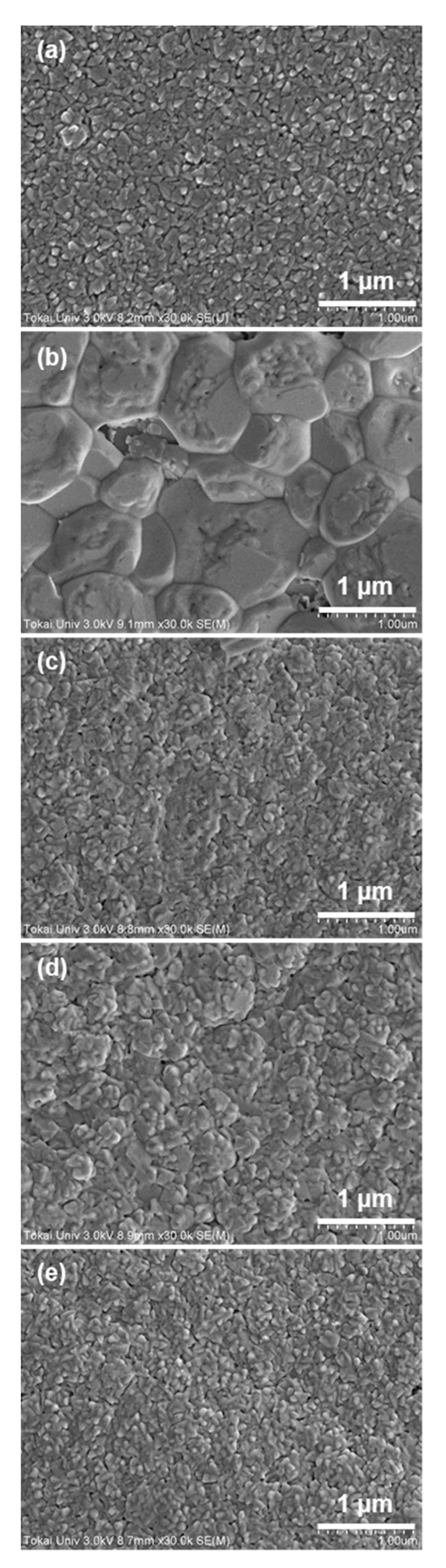
Figure 2.
Atomic composition of the formed Bi2Te3 thin films with different temperature increase rates determined from electron probe microanalyzer (EPMA).
Figure 2.
Atomic composition of the formed Bi2Te3 thin films with different temperature increase rates determined from electron probe microanalyzer (EPMA).
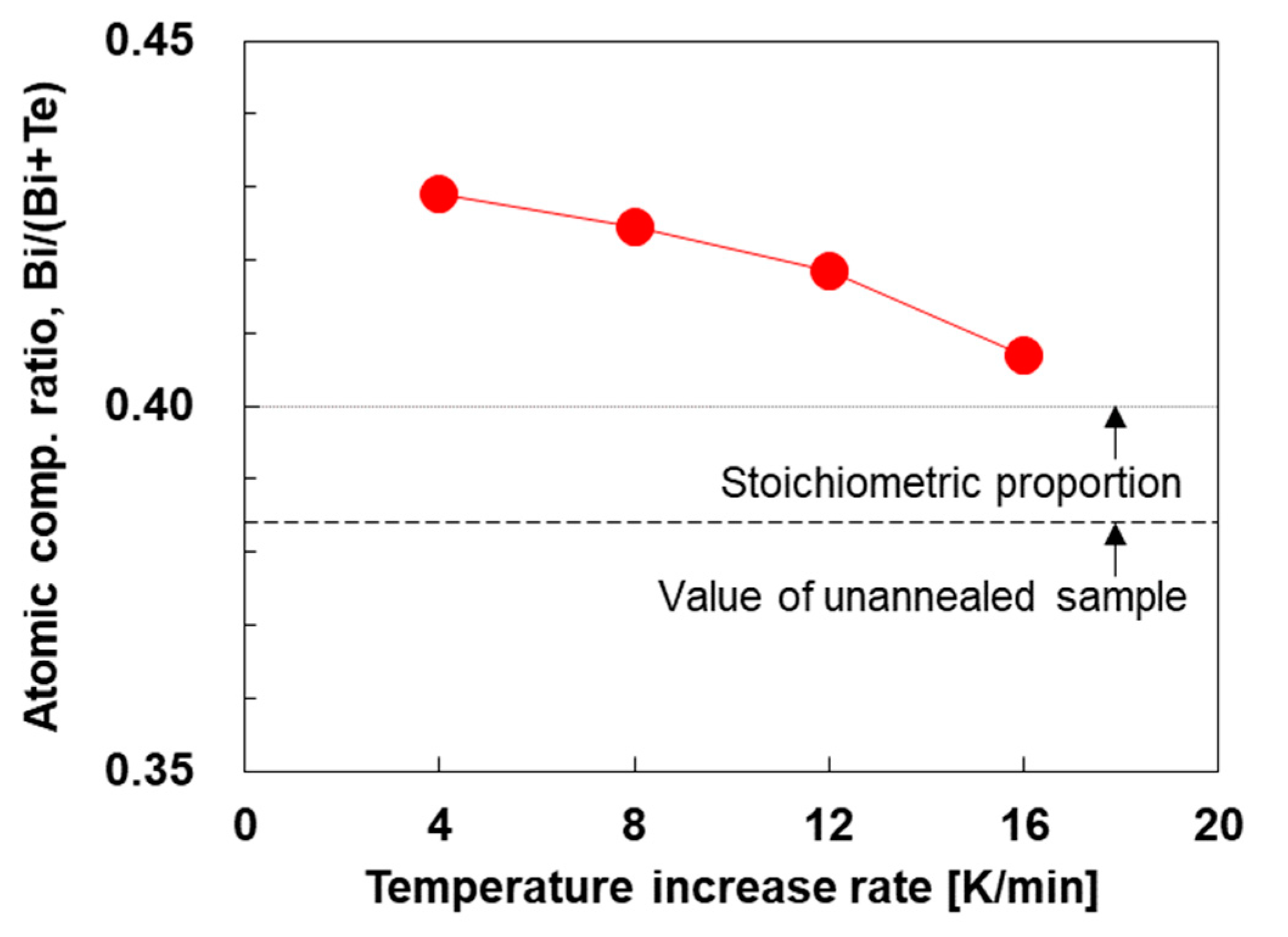
Figure 3.
XRD patterns of the Bi2Te3 thin films without and with heat treatment at different temperature increase rates.
Figure 3.
XRD patterns of the Bi2Te3 thin films without and with heat treatment at different temperature increase rates.
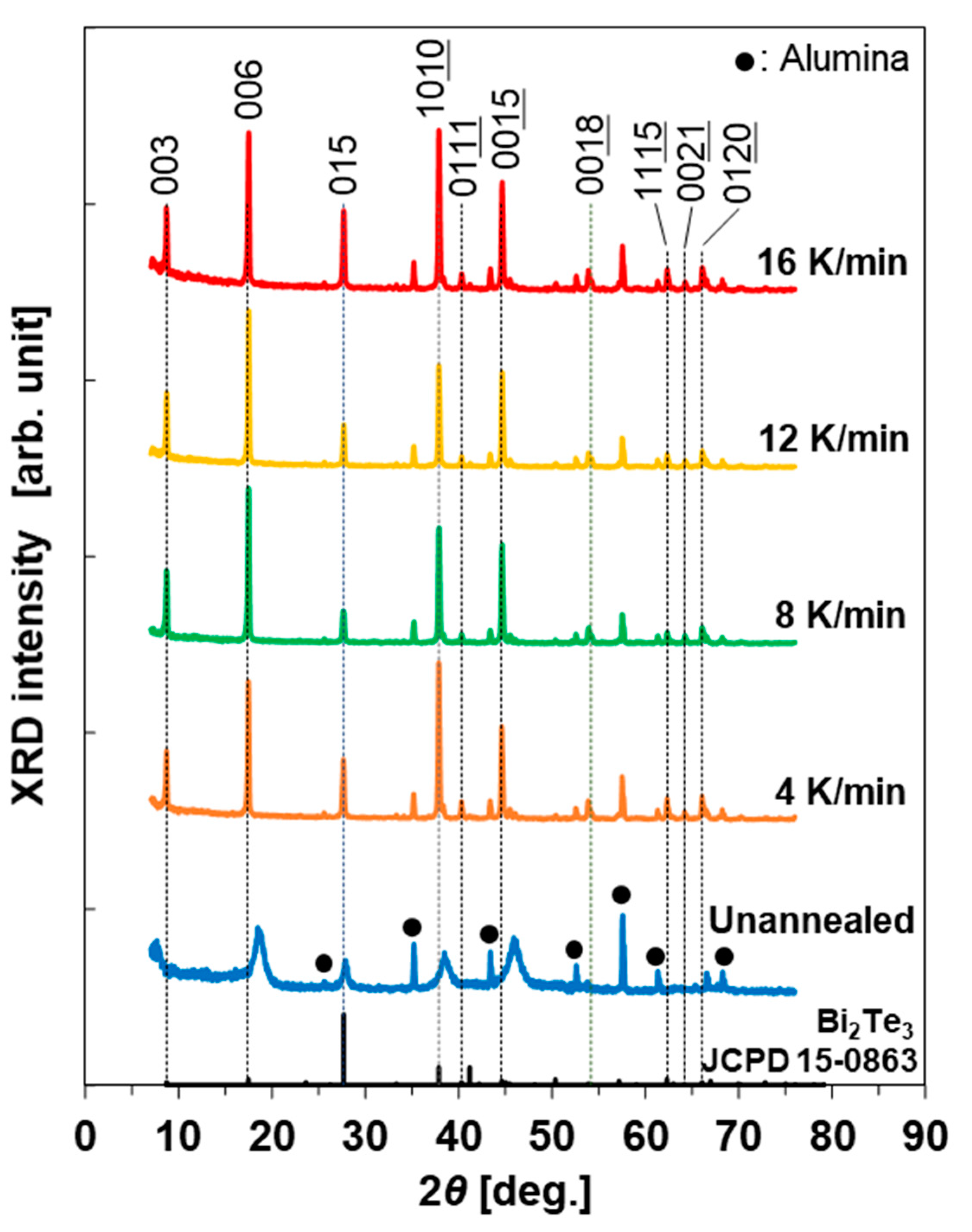
Figure 4.
Crystallographic properties of the various Bi2Te3 thin films determined from the XRD analysis: (a) Lotgering factor F, (b) crystallite size, and (c) lattice constants.
Figure 4.
Crystallographic properties of the various Bi2Te3 thin films determined from the XRD analysis: (a) Lotgering factor F, (b) crystallite size, and (c) lattice constants.

Figure 5.
In-plane measured electrical transport properties of the Bi2Te3 thin films: (a) Seebeck coefficient, (b) electrical conductivity, and (c) power factor.
Figure 5.
In-plane measured electrical transport properties of the Bi2Te3 thin films: (a) Seebeck coefficient, (b) electrical conductivity, and (c) power factor.
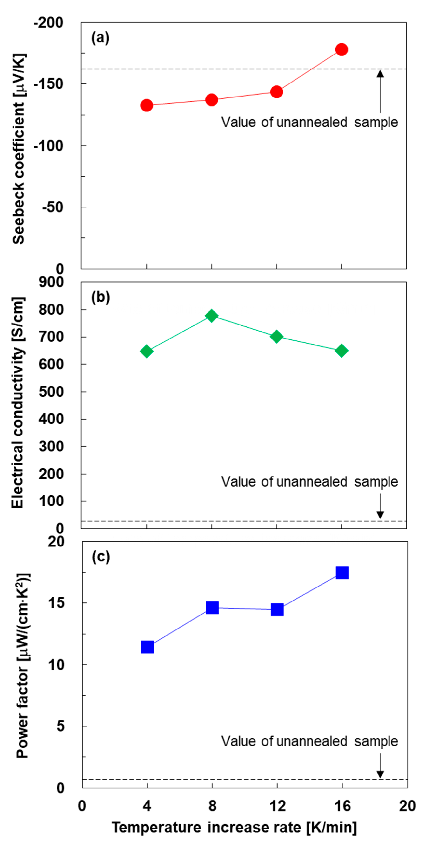
Figure 6.
Calculated in-plane thermal transport properties of the prepared Bi2Te3 thin film.
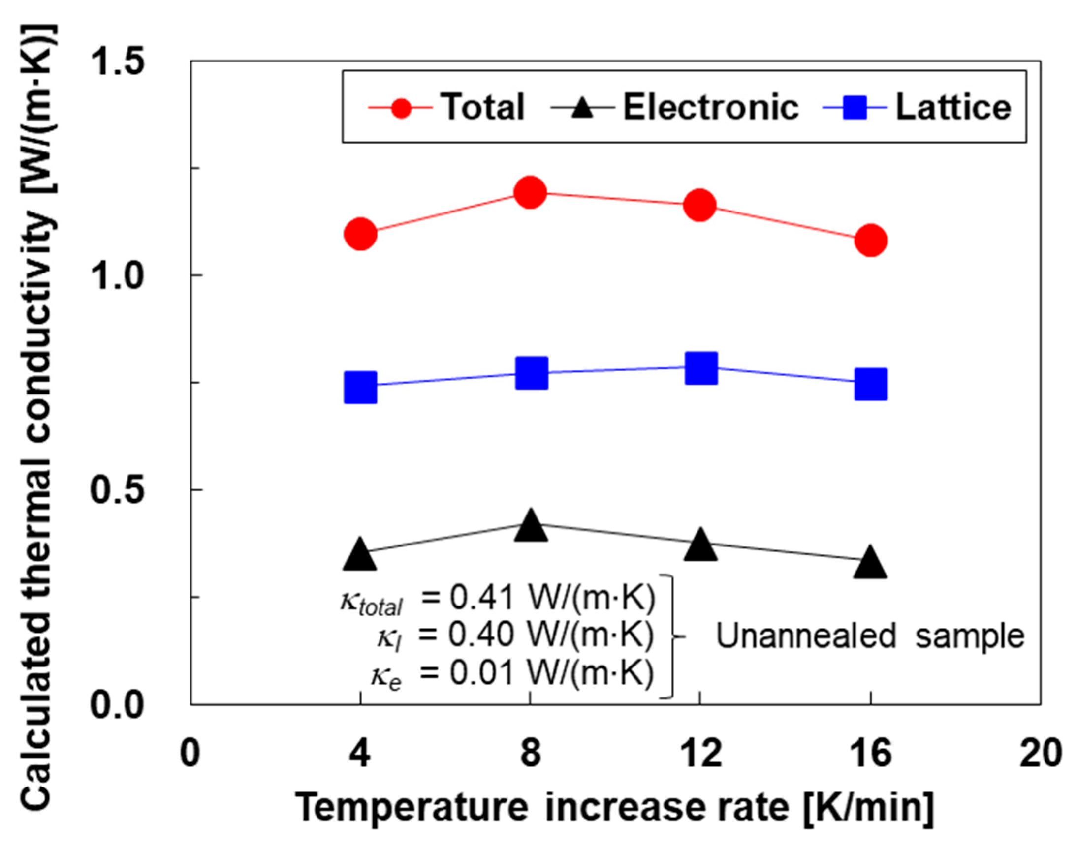
Figure 7.
Dimensionless figure of merit (ZT) of the Bi2Te3 thin films.

Publisher’s Note: MDPI stays neutral with regard to jurisdictional claims in published maps and institutional affiliations. |
© 2021 by the authors. Licensee MDPI, Basel, Switzerland. This article is an open access article distributed under the terms and conditions of the Creative Commons Attribution (CC BY) license (http://creativecommons.org/licenses/by/4.0/).
Share and Cite
MDPI and ACS Style
Norimasa, O.; Kurokawa, T.; Eguchi, R.; Takashiri, M. Evaluation of Thermoelectric Performance of Bi2Te3 Films as a Function of Temperature Increase Rate during Heat Treatment. Coatings 2021, 11, 38. https://doi.org/10.3390/coatings11010038
AMA Style
Norimasa O, Kurokawa T, Eguchi R, Takashiri M. Evaluation of Thermoelectric Performance of Bi2Te3 Films as a Function of Temperature Increase Rate during Heat Treatment. Coatings. 2021; 11(1):38. https://doi.org/10.3390/coatings11010038
Chicago/Turabian StyleNorimasa, Oga, Takuya Kurokawa, Rikuo Eguchi, and Masayuki Takashiri. 2021. "Evaluation of Thermoelectric Performance of Bi2Te3 Films as a Function of Temperature Increase Rate during Heat Treatment" Coatings 11, no. 1: 38. https://doi.org/10.3390/coatings11010038
Note that from the first issue of 2016, this journal uses article numbers instead of page numbers. See further details here.