Effect of Deposition Parameters on the Reactivity of Al/Ni Multilayer Thin Films


Abstract
1. Introduction
2. Materials and Methods
2.1. Deposition Technique
2.2. Characterization Techniques
3. Results and Discussion
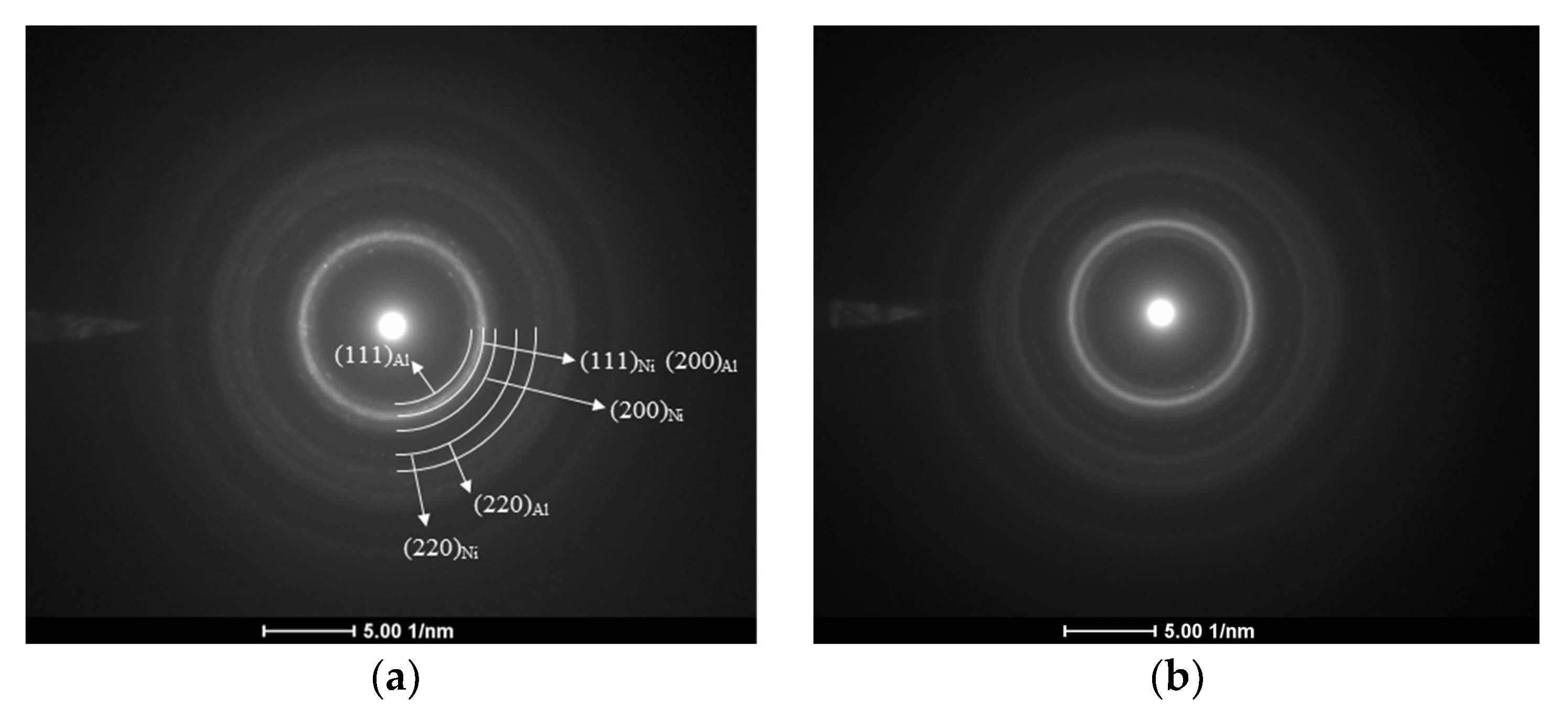
3.1. Phase Analysis
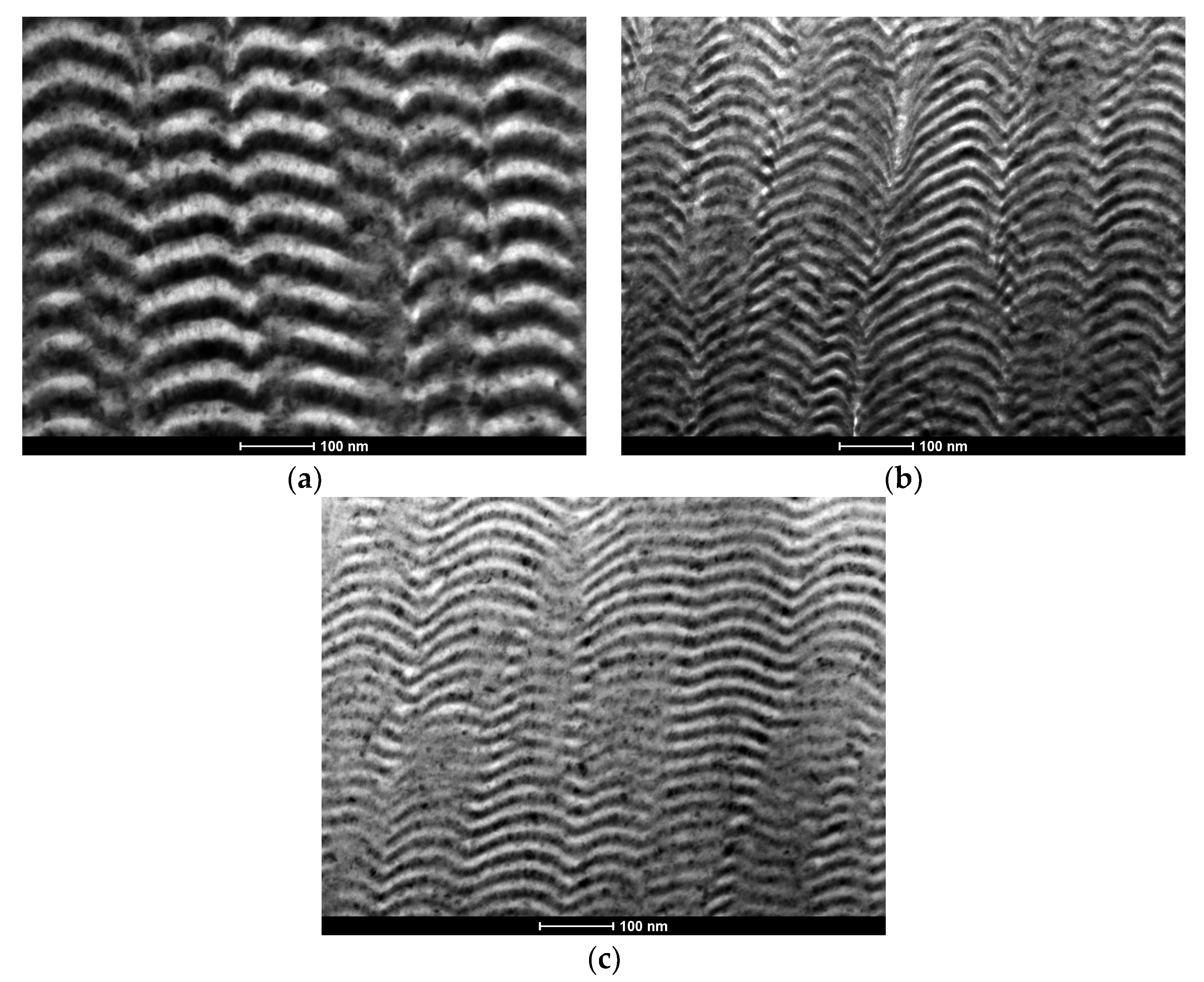
3.2. Microstructure
3.3. Hardness
4. Conclusions
Author Contributions
Funding
Conflicts of Interest
References
- Weihs, T.P. Fabrication and characterization of reactive multilayer foils and films. In Metallic Films for Electronic, Optical and Magnetic Applications—Structure, Processing and Properties, 1st ed.; Barmak, K., Coffey, K., Eds.; Woodhead Publishing Limited: Cambridge, UK, 2014; Volume 3, pp. 160–242. ISBN 978-0-85709-057-7. [Google Scholar]
- Adams, D.P. Reactive multilayers fabricated by vapor deposition: A critical review. Thin Solid Films 2015, 576, 98–128. [Google Scholar] [CrossRef]
- Besnoin, E.; Cerutti, S.; Knio, O.M. Effect of reactant and product melting on self-propagating reactions in multilayer foils. J. Appl. Phys. 2002, 92, 5474–5481. [Google Scholar] [CrossRef]
- Wang, J.; Besnoin, E.; Duckham, A.; Spey, S.J.; Reiss, M.E.; Knio, O.M.; Powers, M.; Whitener, M.; Weihs, T.P. Room-temperature soldering with nanostructured foils. Appl. Phys. Lett. 2003, 83, 3987–3989. [Google Scholar] [CrossRef]
- Duckam, A.; Spey, S.J.; Wang, J.; Reiss, M.E.; Weihs, T.P.; Besnoin, E.; Knio, O.M. Reactive nanostructured foil used as heat source for joining titanium. J. Appl. Phys. 2004, 96, 2336–2342. [Google Scholar] [CrossRef]
- Qiu, X.; Wang, J. Bonding silicon wafers with reactive multilayer foils. Sensor Actuat. A 2008, 141, 476–481. [Google Scholar] [CrossRef]
- Cao, J.; Feng, J.C.; Li, Z.R. Microstructure and fracture properties of reaction-assisted diffusion bonding of TiAl intermetallic with Al/Ni multilayer foils. J. Alloys Compd. 2008, 466, 363–367. [Google Scholar] [CrossRef]
- Rabinovich, O.S.; Grinchuk, P.S.; Andreev, A.M.; Khina, B.B. Conditions for combustion synthesis in nanosized Ni-Al films on a substrate. Phys. Rev. B 2007, 392, 272–280. [Google Scholar] [CrossRef]
- Gavens, A.J.; Van Heerden, D.; Mann, A.B.; Reiss, M.E.; Weihs, T.P. Effect of intermixing on self-propagating exothermic reactions in Al/Ni nanolaminate foils. J. Appl. Phys. 2000, 87, 1255–1263. [Google Scholar] [CrossRef]
- Swain, M.; Singh, S.; Basu, S.; Gupta, M. Effect of interface morphology on intermetallics formation upon annealing of Ni-Al multilayer. J. Alloys Compd. 2013, 484, 257–261. [Google Scholar] [CrossRef]
- Manukyan, K.V.; Tan, W.; de Boer, R.J.; Stech, E.J.; Aprahamian, A.; Wiescher, M.; Rouvimov, S.; Overdeep, K.R.; Shuck, C.E.; Weihs, T.P.; et al. Irradiation-enhanced reactivity of multilayer Al/Ni nanomaterials. ACS Appl. Mater. Interfaces 2015, 7, 11272–11279. [Google Scholar] [CrossRef] [PubMed]
- Politano, O.; Baras, F.; Mukasyan, A.S.; Vadchenko, S.G.; Rogachev, A.S. Microstructure development during NiAl intermetallic synthesis in reactive Ni-Al nanolayers; Numerical investigations vs. TEM observations. Surf. Coat. Technol. 2013, 215, 485–492. [Google Scholar] [CrossRef]
- Ramos, A.S.; Maj, L.; Morgiel, J.; Vieira, M.T. Coating of Tungsten Wire with Ni/Al Multilayers for Self-Healing Applications. Metals 2017, 574, 574. [Google Scholar] [CrossRef]
- ICCD—International Centre for Diffraction Data. Cards 4-0787 and 4-0850 h. Available online: https://www.icdd.com/ (accessed on 2 July 2020).
- Edelstein, A.S.; Everett, R.K.; Richardson, G.Y.; Qadri, S.B.; Altman, E.I.; Foley, J.C.; Perepezko, J.H. Intermetallic phase formation during annealing of Al/Ni multilayers. J. Appl. Phys. 1994, 76, 7850–7859. [Google Scholar] [CrossRef]
- Flores, M.; Muhl, S.; Huerta, L.; Andrade, E. The influence of the period size on the corrosion and the wear abrasion resistance of TiN/Ti multilayers. Surf. Coat. Technol. 2005, 200, 1315–1319. [Google Scholar] [CrossRef]
- Ramos, A.S.; Vieira, M.T.; Serra, C. Ti/Al nanolayered thin films. J. Nanosci. Nanotechnol. 2009, 9, 3627–3632. [Google Scholar] [CrossRef] [PubMed]
- Wu, H.; Mayeshiba, T.; Morgan, D. High-throughput ab-initio dilute solute diffusion database. Sci. Data 2016, 3, 160054. [Google Scholar] [CrossRef] [PubMed]
- Colgan, E.G. A review of thin-film aluminide formation. Mat. Sci. Rep. 1990, 5, 1–44. [Google Scholar] [CrossRef]
- Rothhaar, U.; Oechsner, H.; Scheib, M.; Müller, R. Compositional and structural characterization of temperature-induced solid-state reactions in Al/Ni multilayers. Phys. Rev. B 2000, 61, 974–979. [Google Scholar] [CrossRef]
- Kang, B.C.; Kim, H.Y.; Kwon, O.Y.; Hong, S.H. Bilayer thickness effects on nanoindentation behavior of Ag/Ni multilayers. Scripta Mater. 2007, 57, 703–706. [Google Scholar] [CrossRef]


| Designation | Deposition Time (min) | Rotation Speed (rpm) | Substrate Bias (V) | Ion Gun | Total Thickness * (nm) | Estimated Period (nm) |
|---|---|---|---|---|---|---|
| Λ = 25 | 31 | 3.5 | −40 | OFF | 2700 | 25 |
| Λ = 50 | 32 | 2 | −40 | OFF | 2900 | 45 |
| VS = −80 | 31 | 3.5 | −80 | OFF | 2700 | 25 |
| Ion Gun | 33 | 3 | −40 | ON | 2500 | 25 |
© 2020 by the authors. Licensee MDPI, Basel, Switzerland. This article is an open access article distributed under the terms and conditions of the Creative Commons Attribution (CC BY) license (http://creativecommons.org/licenses/by/4.0/).
Share and Cite
Ramos, A.S.; Simões, S.; Maj, L.; Morgiel, J.; Vieira, M.T. Effect of Deposition Parameters on the Reactivity of Al/Ni Multilayer Thin Films. Coatings 2020, 10, 721. https://doi.org/10.3390/coatings10080721
Ramos AS, Simões S, Maj L, Morgiel J, Vieira MT. Effect of Deposition Parameters on the Reactivity of Al/Ni Multilayer Thin Films. Coatings. 2020; 10(8):721. https://doi.org/10.3390/coatings10080721
Chicago/Turabian StyleRamos, Ana Sofia, Sónia Simões, Lukasz Maj, Jerzy Morgiel, and Maria Teresa Vieira. 2020. "Effect of Deposition Parameters on the Reactivity of Al/Ni Multilayer Thin Films" Coatings 10, no. 8: 721. https://doi.org/10.3390/coatings10080721
APA StyleRamos, A. S., Simões, S., Maj, L., Morgiel, J., & Vieira, M. T. (2020). Effect of Deposition Parameters on the Reactivity of Al/Ni Multilayer Thin Films. Coatings, 10(8), 721. https://doi.org/10.3390/coatings10080721