Control of Lateral Composition Distribution in Graded Films of Soluble Solid Systems A1−xBx by Partitioned Dual-Beam Pulsed Laser Deposition

 ,
,  ,
, 
Abstract
1. Introduction
2. Experiments and Simulation
2.1. Deposition Equipment
2.2. Characterization
2.3. Simulation
3. Single Target Ablation Experiment and Simulation
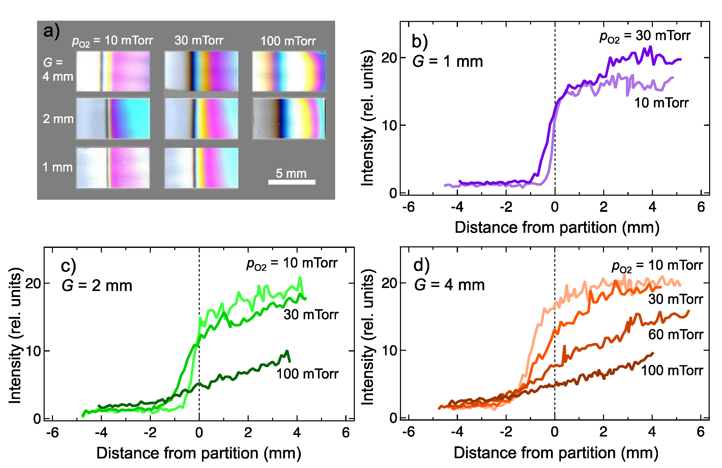
3.1. Experiment
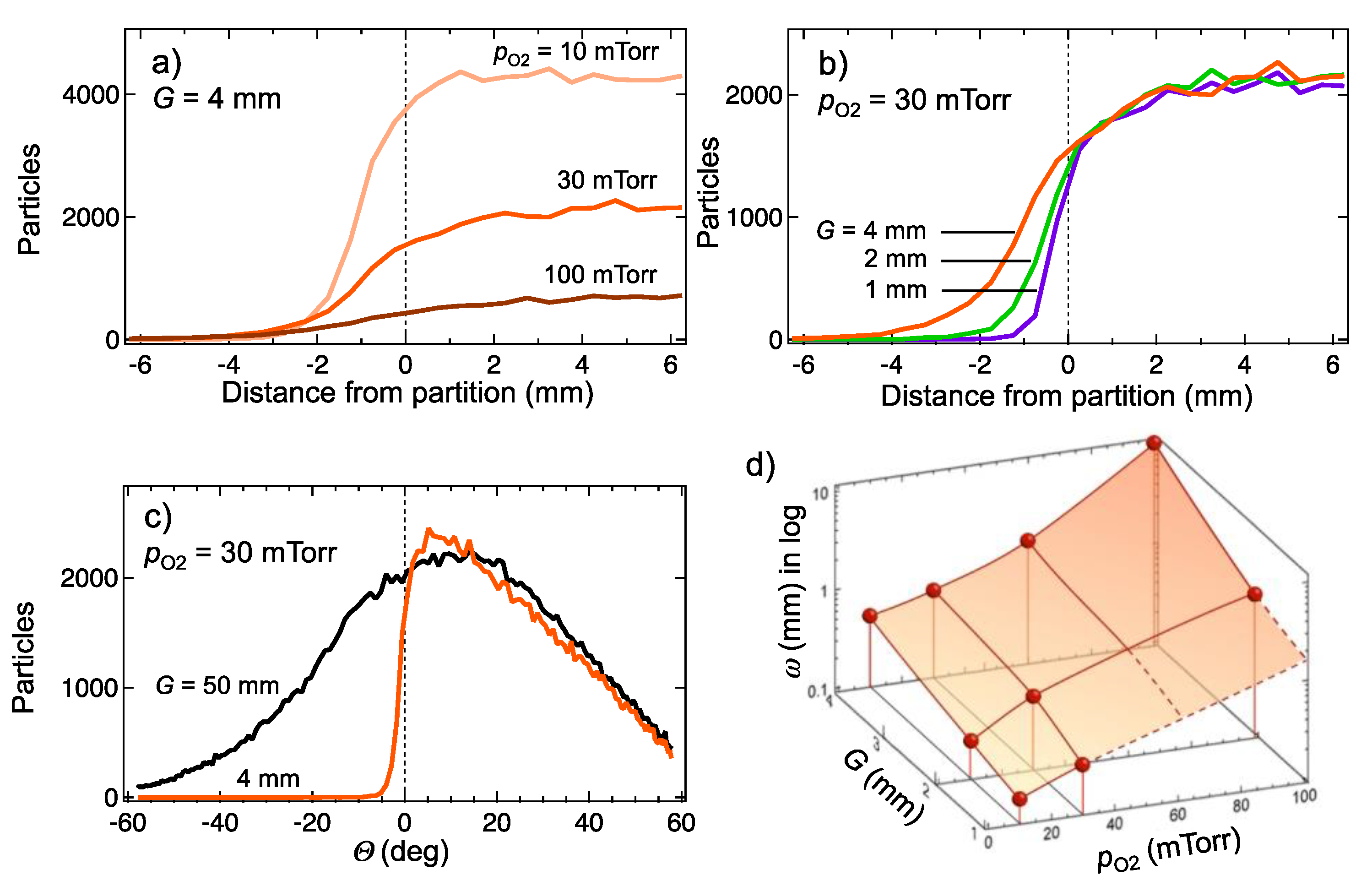
3.2. Simulation
4. Deposition of Compositionally-Graded Films
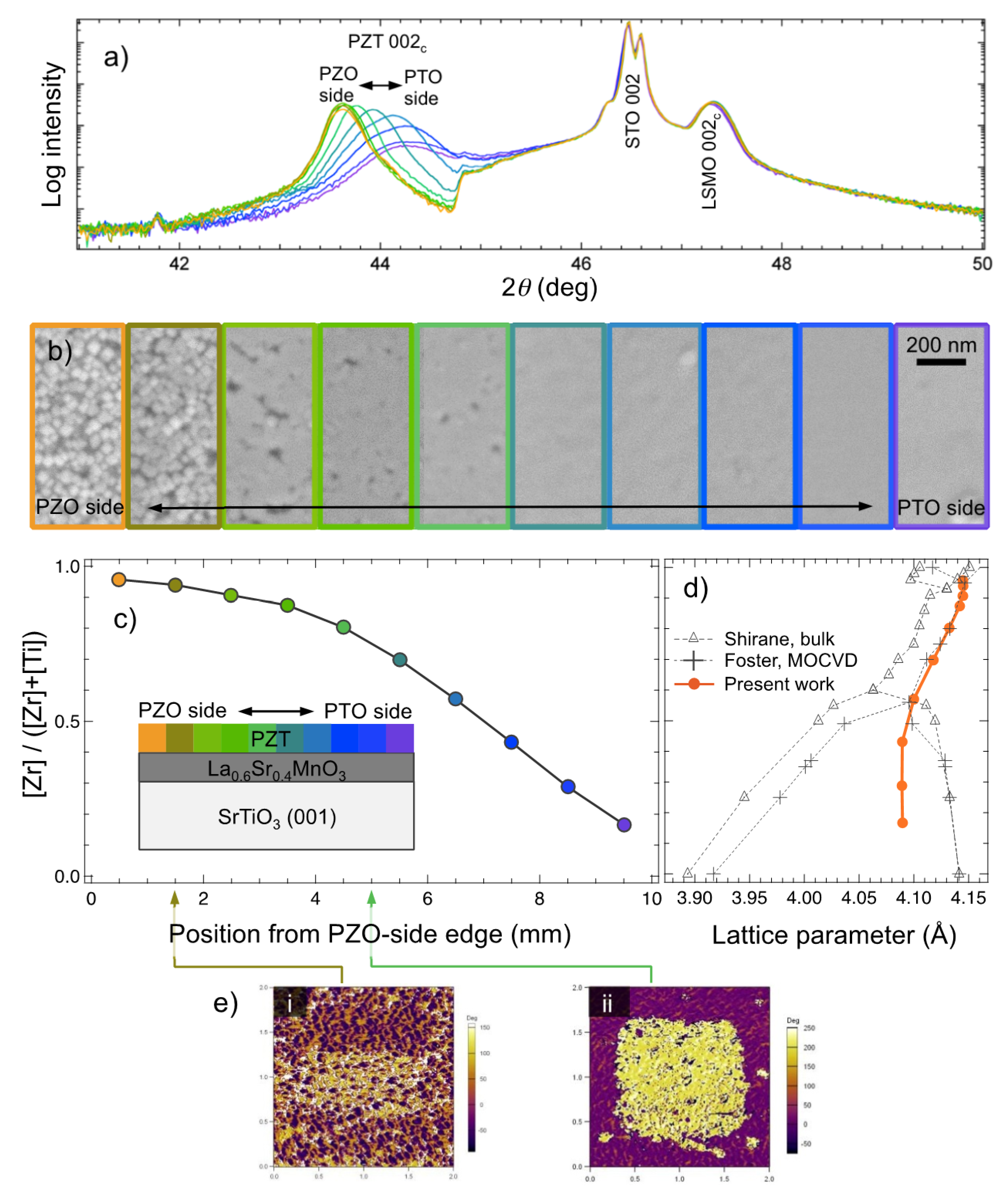
4.1. (1−x)PbTiO3—xPbZrO3
4.2. (1−x)LaMnO3—xLa0.6Sr0.4MnO3
5. Conclusions
Supplementary Materials
Author Contributions
Funding
Acknowledgments
Conflicts of Interest
References
- Jaffe, B.; Cook, W.R.; Jaffe, H. Piezoelectric Ceramics; Academic Press: London, UK, 1971. [Google Scholar]
- Noheda, B.; Gonzalo, J.A.; Cross, L.E.; Guo, R.; Park, S.-E.; Cox, D.E.; Shirane, G. Tetragonal-to-monoclinic phase transition in a ferroelectric perovskite: The structure of PbZr0.52Ti0.48O3. Phys. Rev. B 2000, 61, 8687–8695. [Google Scholar] [CrossRef]
- Park, S.E.; Shrout, T.E. Ultrahigh strain and piezoelectric behavior in relaxor based ferroelectric single crystals. J. Appl. Phys. 1997, 82, 1804–1811. [Google Scholar] [CrossRef]
- Takenaka, T.; Maruyama, K.; Sakata, K. (Bi1/2Na1/2)TiO3-BaTiO3 system for lead-free piezoelectric ceramics. Jpn. J. Appl. Phys. 1991, 30, 2236–2239. [Google Scholar] [CrossRef]
- Yang, S.; Bao, H.; Zhou, C.; Wang, Y.; Ren, X.; Matsushita, Y.; Katsuya, Y.; Tanaka, M.; Kobayashi, K.; Song, X.; et al. Large magnetostriction from morphotropic phase boundary in ferromagnets. Phys. Rev. Lett. 2010, 104, 197201. [Google Scholar] [CrossRef] [PubMed]
- Zhang, N.; Yokota, H.; Glazer, A.M.; Keen, D.A.; Gorfman, S.; Thomas, P.A.; Rena, W.; Yeb, Z.G. Local-scale structures across the morphotropic phase boundary in PbZr1−xTixO3. IUCrJ 2018, 5, 73–81. [Google Scholar] [CrossRef] [PubMed]
- Fang, M.; Rajput, S.; Dai, Z.; Ji, Y.; Hao, Y.; Ren, X. Understanding the mechanism of thermal-stable high-performance piezoelectricity. Acta Mater. 2019, 169, 155–161. [Google Scholar] [CrossRef]
- Gao, J.; Hu, X.; Wang, Y.; Liu, Y.; Zhang, L.; Ke, X.; Zhong, L.; Zhao, H.; Ren, X. Understanding the mechanism of large dielectric response in Pb-free (1−x)Ba(Zr0.2Ti0.8)O3−x(Ba0.7Ca0.3)TiO3 ferroelectric ceramics. Acta Mater. 2017, 125, 77–186. [Google Scholar] [CrossRef]
- Xiang, X.D.; Sun, X.; Briceño, G.; Lou, Y.; Wang, K.A.; Chang, H.; Wallance-Freedman, W.G.; Chen, S.W.; Schultz, P.G. A combinatorial approach to materials discovery. Science 1995, 268, 1738–1740. [Google Scholar] [CrossRef]
- Fukumura, T.; Ohtani, M.; Kawasaki, M.; Okimoto, Y.; Kageyama, T.; Koida, T.; Hasegawa, T.; Tokura, Y.; Koinuma, H. Rapid construction of a phase diagram of doped Mott insulators with a composition-spread approach. Appl. Phys. Lett. 2000, 77, 3426–3428. [Google Scholar] [CrossRef]
- Chang, K.S.; Aronova, M.; Famodu, O.; Takeuchi, I.; Lofland, S.E.; Hattrick-Simpers, J.; Chang, H. Multimode quantitative scanning microwave microscopy of in situ grown epitaxial Ba1−xSrxTiO3 composition spreads. Appl. Phys. Lett. 2001, 79, 4411–4413. [Google Scholar] [CrossRef]
- Christen, H.M.; Silliman, S.D.; Harshavardhan, K.S. Continuous compositional-spread technique based on pulsed-laser deposition and applied to the growth of epitaxial films. Rev. Sci. Instrum. 2001, 72, 2673–2678. [Google Scholar] [CrossRef][Green Version]
- Koinuma, H.; Takeuchi, I. Combinatorial solid-state chemistry of inorganic materials. Nat. Mater. 2004, 3, 429–438. [Google Scholar]
- Venimadhav, A.; Yates, K.A.; Blamire, M.G. Scanning Raman spectroscopy for characterizing compositionally spread films. J. Comb. Chem. 2005, 7, 85–89. [Google Scholar] [CrossRef] [PubMed][Green Version]
- Qiu, J.; Liu, G.Z.; Wolfman, J.; Autret-Lambert, C.; Roger, S.; Gao, J. Structure and dielectric characteristics of continuous composition spread Ba1−xSrxTiO3 thin films by combinatorial pulsed laser deposition. Ceram. Int. 2016, 42, 6408–6412. [Google Scholar] [CrossRef]
- Jaber, N.; Wolfman, J.; Daumont, C.; Négulescu, B.; Ruyter, A.; Feuillard, G.; Bavencoffe, M.; Fortineau, J.; Sauvage, T.; Courtois, B.; et al. Enhancement of piezoelectric response in Ga doped BiFeO3 epitaxial thin films. J. Appl. Phys. 2015, 117, 244107. [Google Scholar] [CrossRef]
- Nagata, T.; Kumaragurubaran, S.; Suzuki, Y.; Takahashi, K.; Ri, S.G.; Tsunekawa, Y.; Suzuki, S.; Chikyow, T. Combinatorial thin film synthesis for developments of new high dielectric constant thin film materials. Trans. Mat. Res. Soc. Jpn. 2018, 43, 249–254. [Google Scholar] [CrossRef]
- Hussey, B.W.; Gupta, A. Synthesis of YBa2Cu3O7–δ films from separate oxide targets. J. Appl. Phys. 1992, 72, 287–289. [Google Scholar] [CrossRef]
- Ito, A.; Machida, A.; Obara, M. Cobalt doping in BaTiO3 thin films by two-target pulsed KrF laser ablation with in situ laser annealing. Appl. Phys. Lett. 1997, 70, 3338–3340. [Google Scholar] [CrossRef]
- Schenck, P.K.; Kaiser, D.L.; Davydov, A.V. High throughput characterization of the optical properties of compositionally graded combinatorial films. Appl. Surf. Sci. 2004, 223, 200–205. [Google Scholar] [CrossRef]
- Keller, D.A.; Ginsburg, A.; Barad, H.-N.; Shimanovich, K.; Bouhadana, Y.; Rosh-Hodesh, E.; Takeuchi, I.; Aviv, H.; Tischler, Y.R.; Anderson, A.Y.; et al. Utilizing pulsed laser deposition lateral inhomogeneity as a tool in combinatorial material science. ACS Comb. Sci. 2015, 17, 209–216. [Google Scholar] [CrossRef]
- Itina, T.E.; Marine, W.; Autric, M. Monte Carlo simulation of pulsed laser ablation from two-component target into diluted ambient gas. J. Appl. Phys. 1997, 82, 3536–3542. [Google Scholar] [CrossRef]
- Saenger, K.L. Pulsed Laser Deposition of Thin Films; Chrisey, D.B., Hubler, G.K., Eds.; Wiley: New York, NY, USA, 1994; pp. 199–227. [Google Scholar]
- Singh, R.K. Spatial thickness variations in laser-deposited thin films. Mater. Sci. Eng. B 1997, 45, 180–185. [Google Scholar] [CrossRef]
- Rashidian Vaziri, M.R.; Hajiesmaeilbaigi, F.; Maleki, M.H. Monte Carlo simulation of the subsurface growth mode during pulsed laser deposition. J. Appl. Phys. 2011, 110, 043304. [Google Scholar] [CrossRef]
- Urushibara, A.; Moritomo, Y.; Arima, T.; Asamitsu, A.; Kido, G.; Tokura, Y. Insulator-metal transition and giant magnetoresistance in La1−xSrxMnO3. Phys. Rev. B 1995, 51, 14103–14109. [Google Scholar] [CrossRef] [PubMed]
- Coey, J.M.D.; Viret, M.; von Molnar, S. Mixed-valence manganites. Adv. Phys. 1999, 48, 167–293. [Google Scholar] [CrossRef]
- Bond, W.L. Notes on solution of problems in odd job vapor coating. J. Opt. Soc. Am. 1954, 44, 429–438. [Google Scholar] [CrossRef]
- Bassim, N.D.; Schenck, P.K.; Otani, M.; Oguchi, H. Model, prediction, and experimental verification of compositionand thickness in continuous spread thin film combinatorial libraries grown by pulsed laser deposition. Rev. Sci. Instr. 2007, 78, 072203. [Google Scholar] [CrossRef]
- Shirane, G.; Suzuki, K. Crystal structure of Pb(Zr-Ti)O3. J. Phys. Soc. Jpn. 1952, 7, 333. [Google Scholar] [CrossRef]
- Foster, C.M.; Bai, G.-R.; Csencsits, R.; Vetrone, J.; Jammy, R.; Wills, L.A.; Carr, E.; Amano, J. Single-crystal Pb(ZrxTi1−x)O3 thin films prepared by metal-organic chemical vapor deposition: Systematic compositional variation of electronic and optical properties. J. Appl. Phys. 1997, 81, 2349–2357. [Google Scholar] [CrossRef]
- Wiedenhorst, B.; Höfener, C.; Lu, Y.; Klein, J.; Alff, L.; Gross, R.; Freitag, B.H.; Mader, W. Strain effects and microstructure of epitaxial manganite thin films and heterostructures. Appl. Phys. Lett. 1999, 74, 3636–3638. [Google Scholar] [CrossRef]
- Wu, W.; Wong, K.H.; Choy, C.L.; Zhang, Y.H. Top-interface-controlled fatigue of epitaxial Pb(Zr0.52Ti0.48)O3 ferroelectric thin films on La0.7Sr0.3MnO3 electrodes. Appl. Phys. Lett. 2000, 77, 3441–3443. [Google Scholar] [CrossRef]
- Konishi, Y.; Fang, Z.; Izumi, M.; Manako, T.; Kasai, M.; Kuwahara, H.; Kawasaki, M.; Terakura, K.; Tokura, Y. Orbital-state-mediated phase-control of manganites. J. Phys. Soc. Jpn. 1999, 68, 3790–3793. [Google Scholar] [CrossRef]
- Song, J.H.; Susaki, T.; Hwang, H.Y. Enhanced thermodynamic stability of epitaxial oxide thin films. Adv. Mater. 2008, 20, 2528–2532. [Google Scholar] [CrossRef]
- Roqueta, J.; Pomar, A.; Balcells, L.; Frontera, C.; Valencia, S.; Abrudan, R.; Bozzo, B.; Konstantinović, Z.; Santiso, J.; Martínez, B. Strain-engineered ferromagnetism in LaMnO3 thin films. Cryst. Growth Des. 2015, 15, 5332–5337. [Google Scholar] [CrossRef]


© 2020 by the authors. Licensee MDPI, Basel, Switzerland. This article is an open access article distributed under the terms and conditions of the Creative Commons Attribution (CC BY) license (http://creativecommons.org/licenses/by/4.0/).
Share and Cite
Sakai, J.; Roque, J.M.C.; Vales-Castro, P.; Padilla-Pantoja, J.; Sauthier, G.; Catalan, G.; Santiso, J. Control of Lateral Composition Distribution in Graded Films of Soluble Solid Systems A1−xBx by Partitioned Dual-Beam Pulsed Laser Deposition. Coatings 2020, 10, 540. https://doi.org/10.3390/coatings10060540
Sakai J, Roque JMC, Vales-Castro P, Padilla-Pantoja J, Sauthier G, Catalan G, Santiso J. Control of Lateral Composition Distribution in Graded Films of Soluble Solid Systems A1−xBx by Partitioned Dual-Beam Pulsed Laser Deposition. Coatings. 2020; 10(6):540. https://doi.org/10.3390/coatings10060540
Chicago/Turabian StyleSakai, Joe, José Manuel Caicedo Roque, Pablo Vales-Castro, Jessica Padilla-Pantoja, Guillaume Sauthier, Gustau Catalan, and José Santiso. 2020. "Control of Lateral Composition Distribution in Graded Films of Soluble Solid Systems A1−xBx by Partitioned Dual-Beam Pulsed Laser Deposition" Coatings 10, no. 6: 540. https://doi.org/10.3390/coatings10060540
APA StyleSakai, J., Roque, J. M. C., Vales-Castro, P., Padilla-Pantoja, J., Sauthier, G., Catalan, G., & Santiso, J. (2020). Control of Lateral Composition Distribution in Graded Films of Soluble Solid Systems A1−xBx by Partitioned Dual-Beam Pulsed Laser Deposition. Coatings, 10(6), 540. https://doi.org/10.3390/coatings10060540