Article

Transparent Conductive p-Type Cuprous Oxide Films in Vis-NIR Region Prepared by Ion-Beam Assisted DC Reactive Sputtering

1
The Key Lab of Guangdong for Modern Surface Engineering Technology, National Engineering Laboratory for Modern Materials Surface Engineering Technology, Guangdong Institute of New Materials, Guangzhou 510651, China
2
Shandong Key Laboratory of Optical Astronomy and Solar-Terrestrial Environment, School of Space Science and Physics, Shandong University, Weihai 264209, China
3
School of Mechanical, Electrical & Information Engineering, Shandong University, Weihai 264209, China
4
Department of Materials Engineering and Center for Plasma and Thin Film Technologies, Ming Chi University of Technology, Taipei 243, Taiwan
5
Institute of Materials Science and Engineering, National Taiwan University, Taipei 106, Taiwan
*
Authors to whom correspondence should be addressed.
Coatings 2020, 10(5), 473; https://doi.org/10.3390/coatings10050473
Submission received: 23 April 2020 / Revised: 5 May 2020 / Accepted: 7 May 2020 / Published: 13 May 2020
(This article belongs to the Special Issue Magnetron Sputtering Deposited Thin Films and Its Applications)

Abstract

:
Cu2O thin film has been widely studied due to its intrinsic p-type conductivity. It can be used as p-type transparent conductive electrode or hole transport layer in various potential applications. However, its intrinsic p-type conductivity is very limited, which needs to be optimized by introducing acceptor defects. In this work, the electrical properties of the Cu2O films was improved through introducing interstitial oxygen in the films those were deposited via direct current sputtering assisted by oxygen ion beam. The results show that with oxygen ion beam current increase, the carrier concentration effectively improves. However, with more interstitial oxygen introduced, the film’s crystallinity significantly reduces, as well as the carrier mobility decreases. Meanwhile, all of the Cu2O films present moderate transmittance in the visible region (400–800 nm), but ideal transmittance in the near infrared (NIR) light region (800–2500 nm). When compared with the strong reflection of the n-type transparent conductive film to the near infrared light, the Cu2O film is transparent conductive in NIR region, which expands its application in the fabrication of NIR electrical devices.

1. Introduction

The transparent conductive oxides (TCOs) combined high optical transmittance and ideal electrical conductivity are widely used in various fields, for example, flat panel displays, touch screens, transparent electrodes, and so on [1,2,3]. However, the currently widely used TCO are mostly n-type semiconductors, such as SnO2:F (FTO), In2O3:Sn (ITO), ZnO:In,Ga (IGZO), etc. [4,5,6]. Their transmittance in the visible region can reach more than 85%, while their conductivity can achieve 103 S·cm−1, which satisfy the above mentioned application requirements well. However, in the near infrared (NIR) region (800–2500 nm), the transmittance of these n-type TCOs drops sharply [7,8]. For instance, the transmittance of ITO decreases rapidly beyond 1200 nm, although its band gap is higher than 3.0 eV [9]. This severely restricts the application of transparent conductive materials in the NIR region, such as in infrared detection, infrared imaging, and infrared guidance system, etc. In addition, in the photovoltaic field, the current used transparent electrodes on the surface of the solar cell generally possess high transmittance in visible light region, but they have a dramatically deteriorated transmittance in NIR light region. This behavior results in that the NIR light (~50% solar power) cannot be effectively used. Therefore, improving the transmittance of TCO material in the NIR region is full of significance for developing novel optoelectronic devices.
The transmittance of TCOs in NIR region is related to their plasma wavelength (λp), which can be calculated according to the Drude model [10]:
λ p = 2 π C ( ε 0 ε m c * e 2 N m ) 1 / 2
where C is the velocity of light, ε0 and ε are the permittivity of free space and the high-frequency permittivity, respectively. mc* is the conductivity effective mass, e is the electron charge, and Nm is the carrier concentration. As the model predicted, with the carrier concentration increase or the conductivity effective mass decreases, the plasma wavelength λp shifts to the shorter wavelength. As in n-type TCOs, the conductivity effective mass is normally below 0.4 me, while their carrier concentration is very high and even presents degenerate characteristics [11,12,13]. Thus, the plasma wavelength of n-type TCO normally falls in the NIR region, and n-type TCOs possess poor transmittance in this region.
Cu-based oxides have recently attracted increasing attention [14,15,16]. The band gap of intrinsic p-type Cu2O is about 2.4–2.8 eV, allowing for part of visible light to pass through [17,18]. At the same time, its conductivity effective mass of about 0.7 me is much higher than that of the traditional n-type TCOs [19]. Therefore, its plasma wavelength can still fall in mid-infrared or even far-infrared region, even if a higher carrier concentration is achieved. As a result, Cu2O exhibits excellent light transmittance in the NIR region. In addition, the simple structure, non-toxic, and stable characteristics make Cu2O suitable to be used in various applications [20,21]. Indeed, it is an ideal vis-NIR transparent conductive material.
In the current work, the Cu2O films were deposited by magnetron sputtering technique under oxygen-rich conditions. Oxygen ion beam was employed during the deposition process, so as to improve the oxygen amount in the films, thereby increasing the acceptor defects concentration, and further enhancing the film’s electrical performance. The influence of the oxygen ion beam current on the structure and optoelectronic properties of Cu2O films was discussed in detail. Subsequently, a transparent conductive Cu2O film in vis-NIR region can be realized through optimizing the deposition parameters.

2. Materials and Methods

Cu2O films with a thickness within 420–450 nm were deposited on glass substrates from pure copper targets (purity 99.99%) by reactive magnetron sputtering with DC power supply at room temperature. The oxygen ion source was used to assist the deposition process in order to improve the oxygen amount in the films. The oxygen ion beam current (IO₂) is varied (0–5.0 A) to adjust the oxygen amount in the films. Before the deposition, the background of the reactive chamber was pre-pumped to 10−5 Pa. Subsequently, the gas mixture of Ar + O2 was introduced into the chamber. The oxygen flow ratio is fixed at 10%, while the gas flow rates of Ar and O2 are 180 sccm and 20 sccm, respectively. The working pressure is fixed at 1.0 Pa. During the deposition, the pulsed frequency of the power supply was fixed at 50 kHz, while the pulse off-time maintains at 5 μs. The deposition process maintains 15 min. After the deposition, all of the films were annealed at 423 K for 20 min in air ambient.
The film’s thickness was determined by surface profilometer (Ambios Technology Company, Santa Cruz, NM, USA). Energy-dispersive spectroscopy confirmed the film’s composition (EDS, Nova Nano SEM 450, Hillsboro, OR, USA). The phase structures were investigated by X-ray diffractometer (XRD, Rigaku Ultima IV, Rigaku, Tokyo, Japan). The film’s top surface morphology was observed by scanning electron microscope (SEM, Nova Nano SEM 450, Hillsboro, OR, USA). Hall effect analysis with van der Pauw’s configuration (Keithley-4200 SCS, Beaverton, OR, USA) was used in order to analyze the film’s electrical properties. The film’s optical properties in the visible region and NIR region were characterized by UV-Vis-NIR spectrophotometer (PerkinElmer LAMBDA 1050, Waltham, MA, USA).

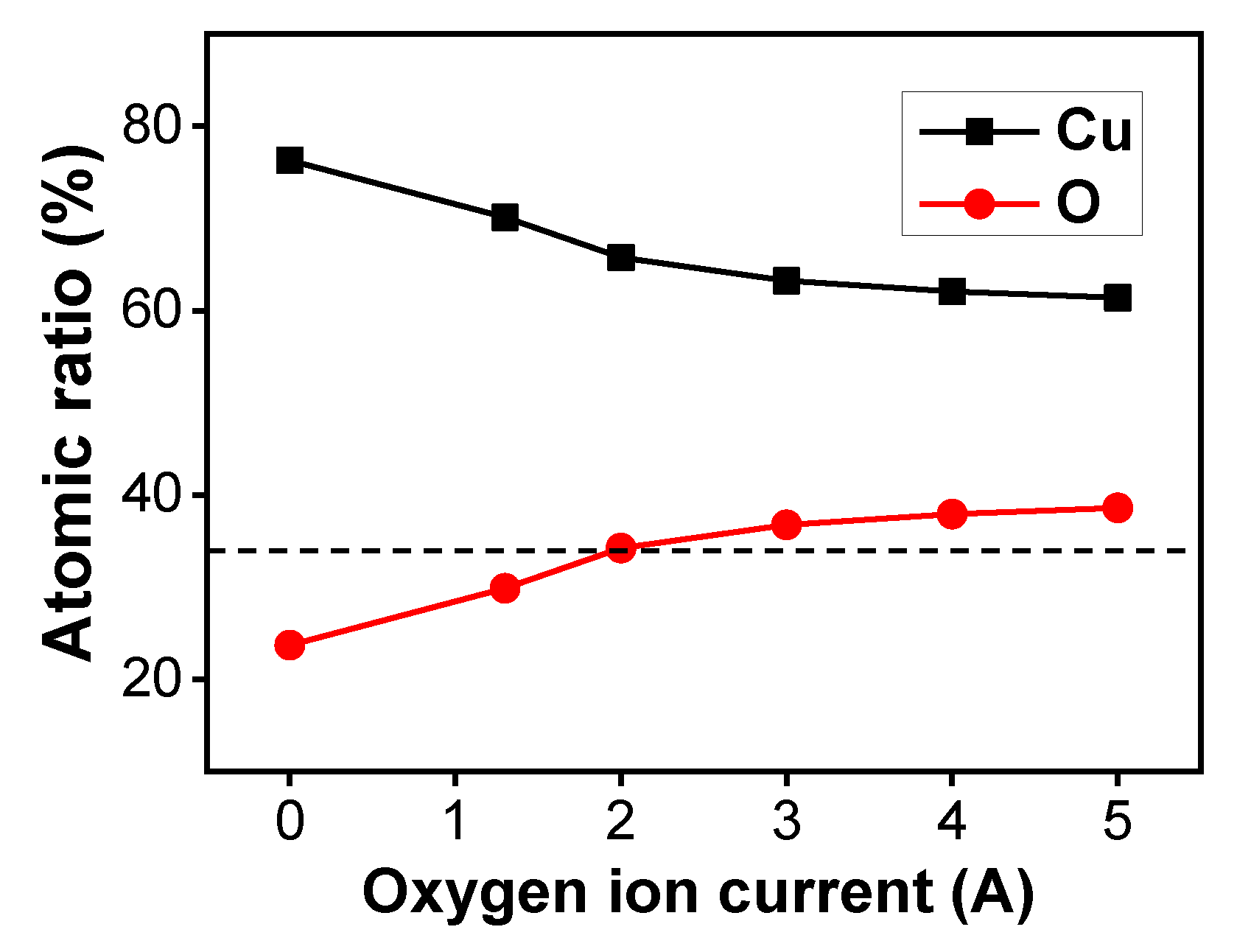
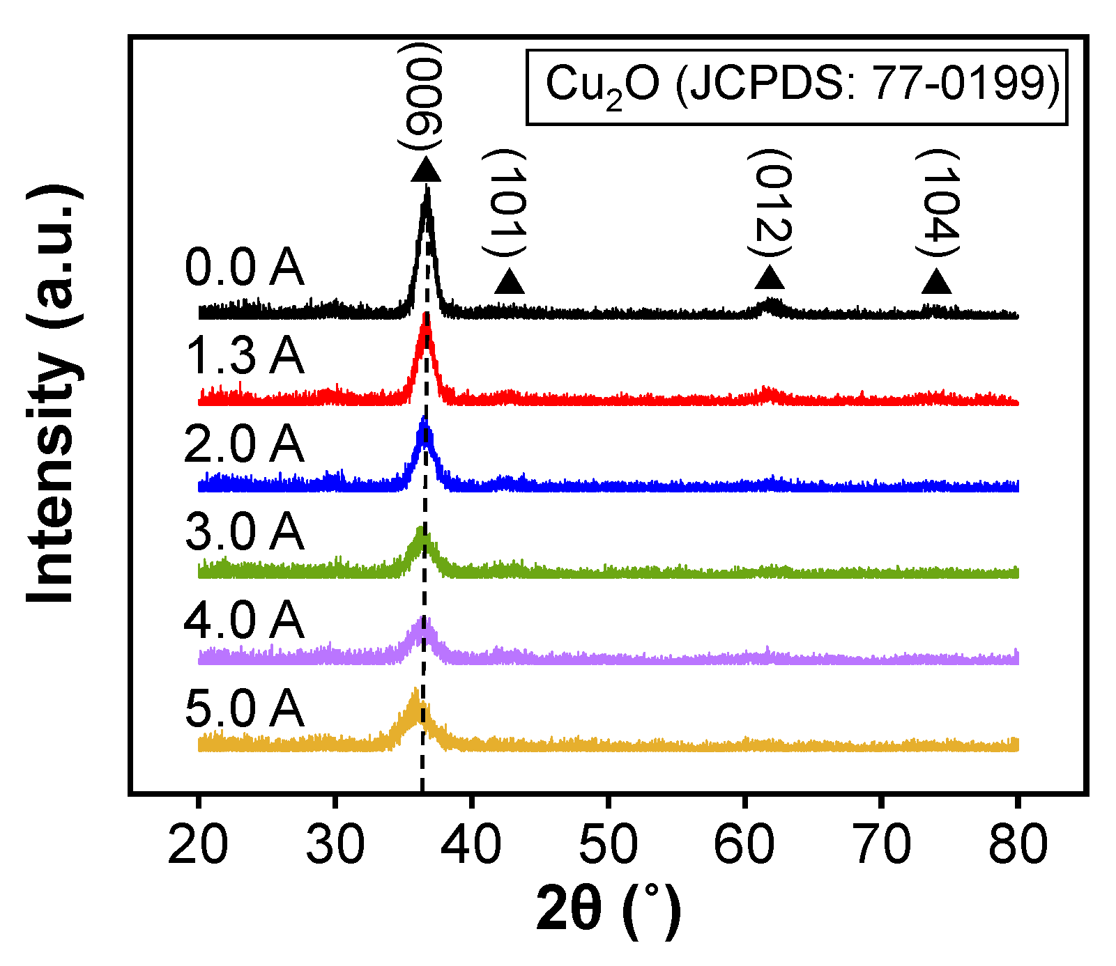
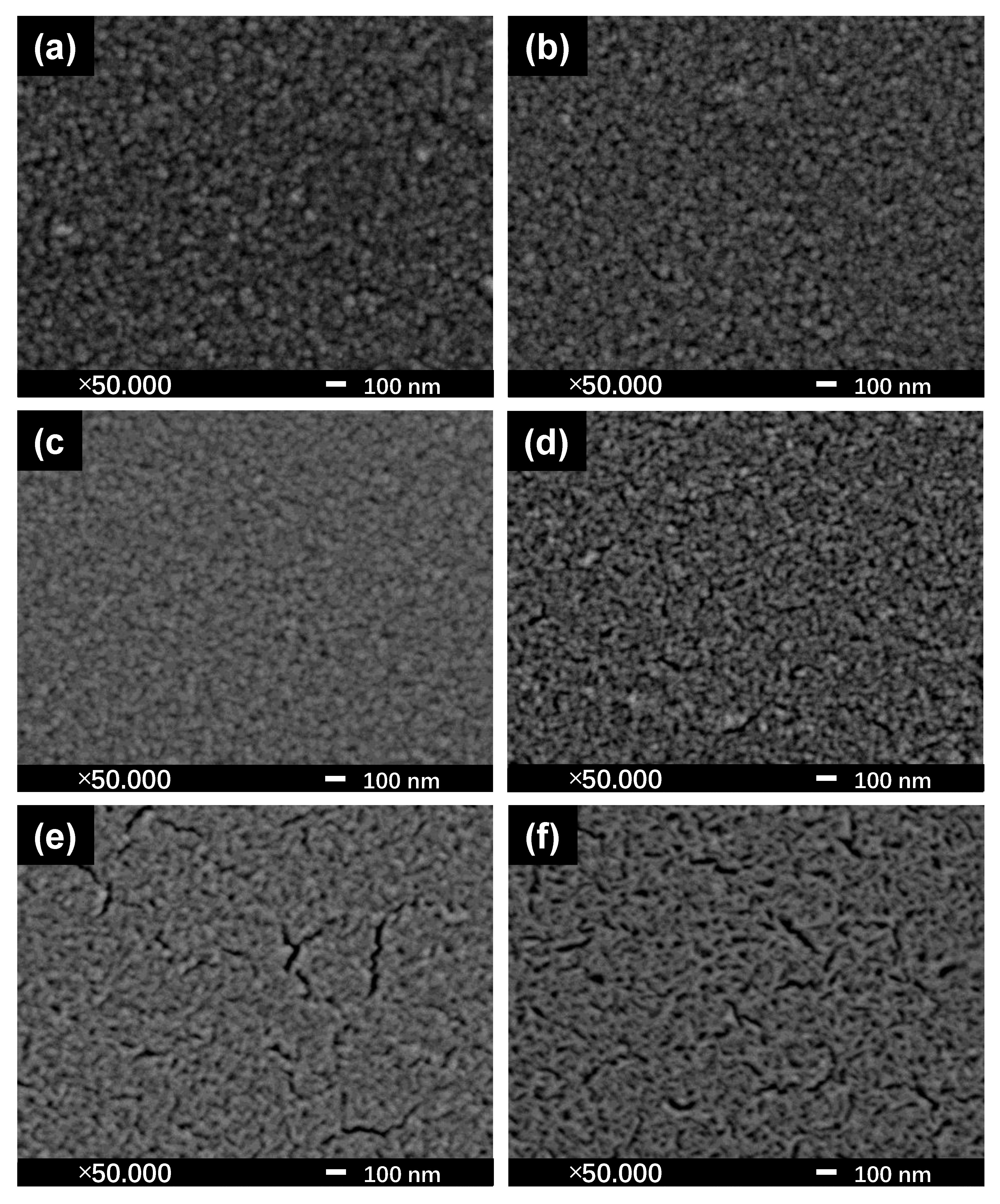
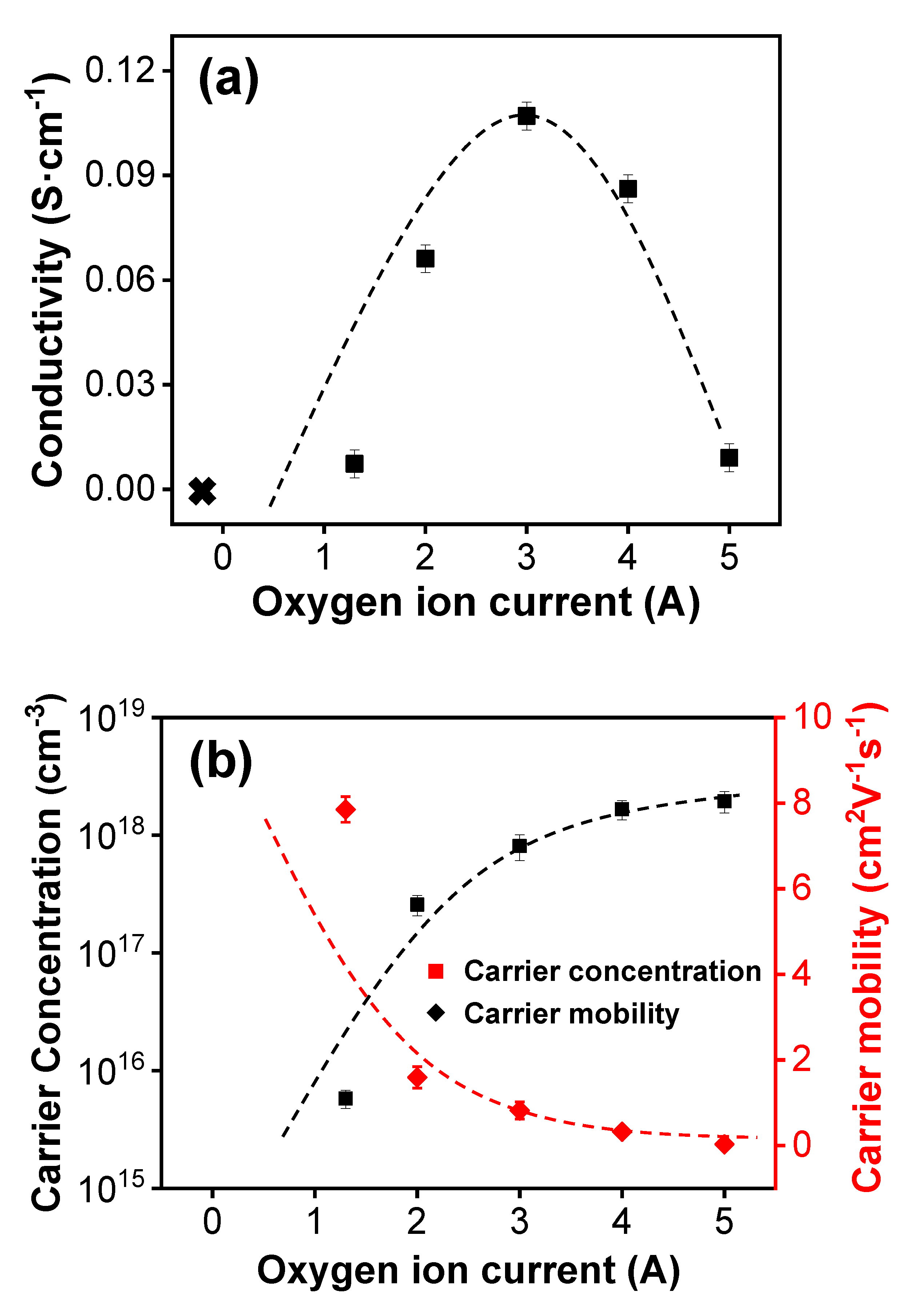
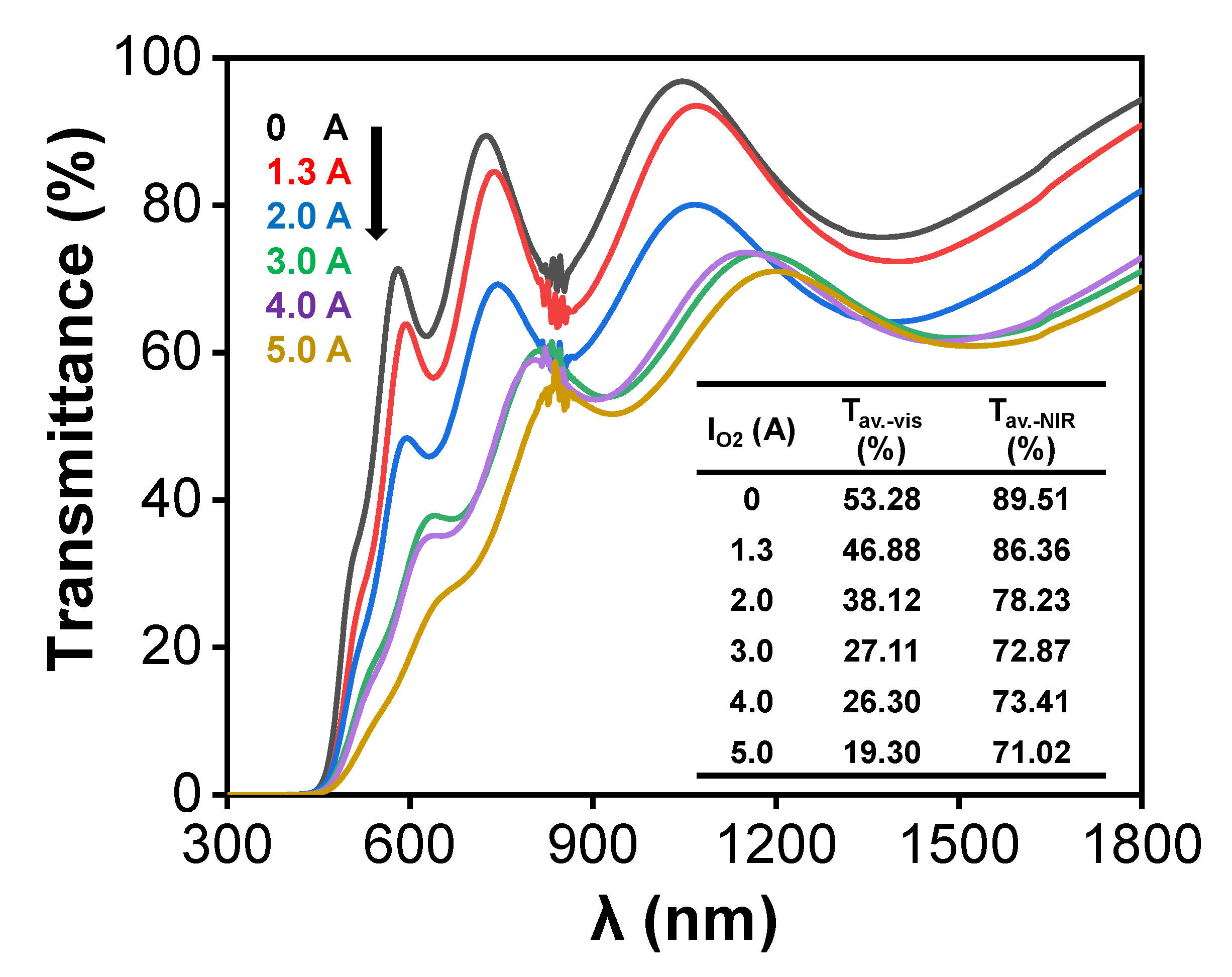
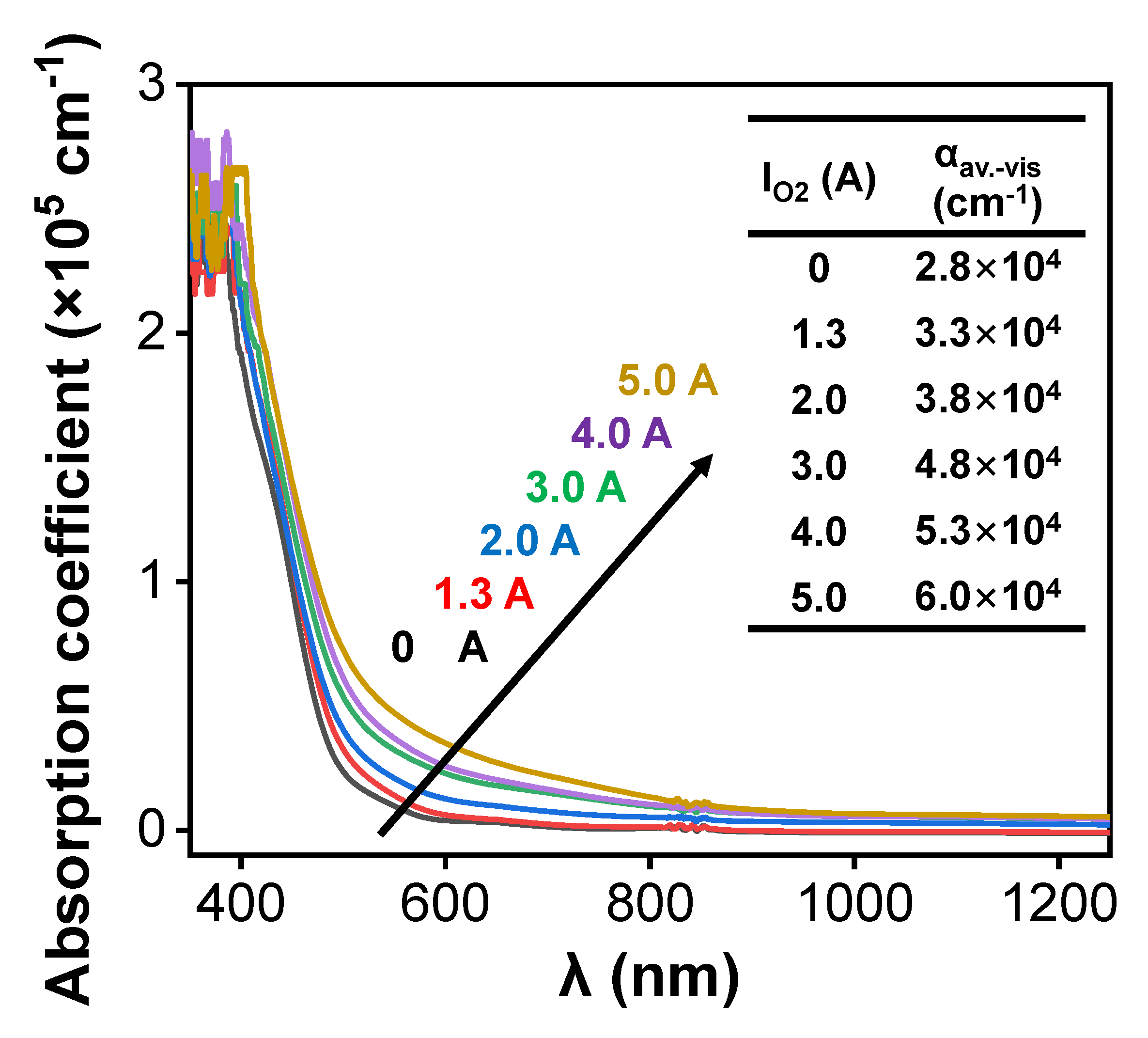
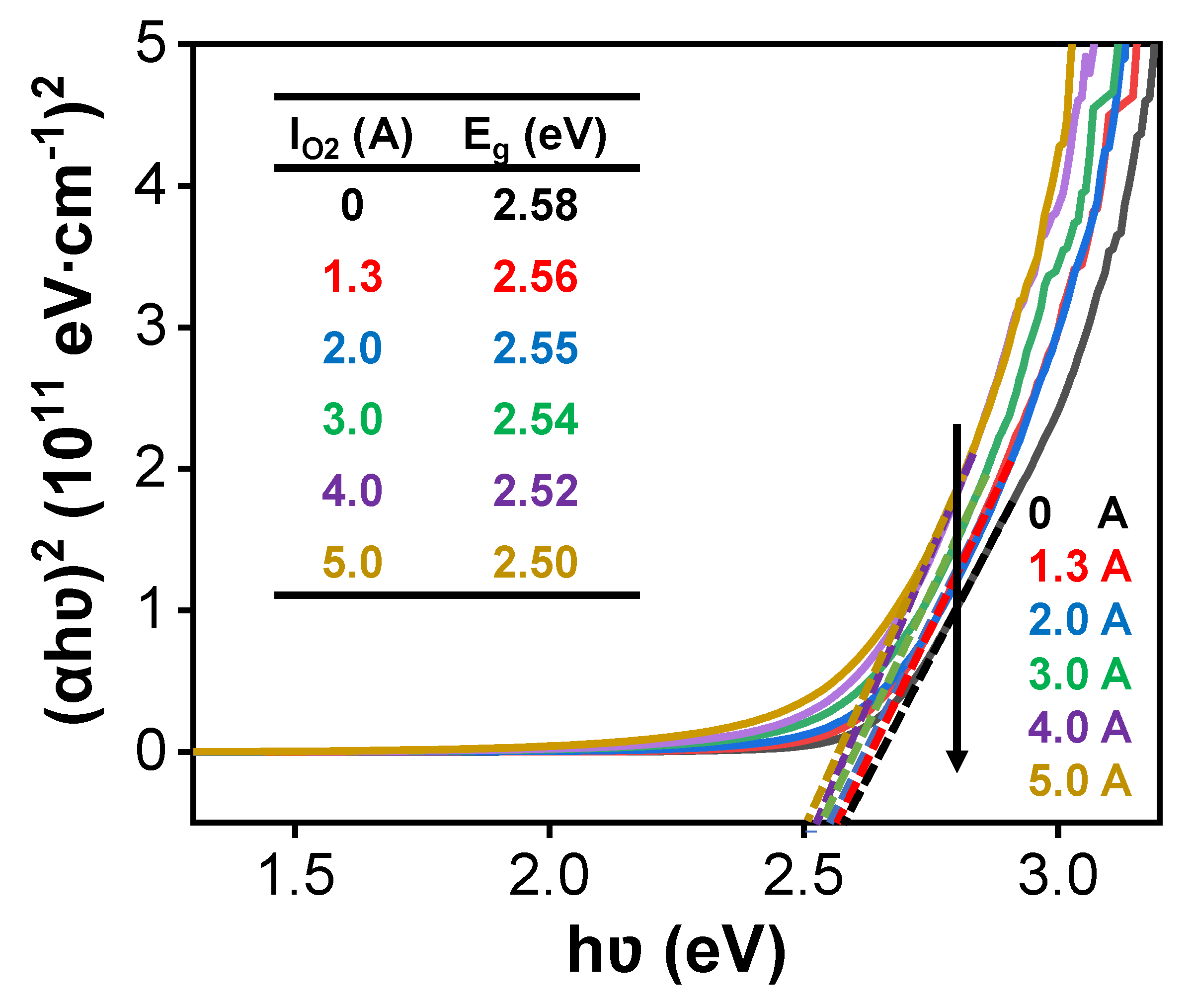
3. Results and Discussion

Figure 1 illustrates the evolution of the film’s composition as oxygen ion beam current (IO₂) increase. It is demonstrated that the film deposited under Ar + O2 ambience without oxygen ion beam assisted is O-deficient. For the films deposited with oxygen ion beam assisted, the oxygen amount in the films gradually increases, until the film is oxygen-rich. For Cu2O film, the intrinsic acceptor defects are copper vacancies or interstitial oxygen [22,23]. Thus, oxygen-rich condition is beneficial for fabricating Cu2O film with higher interstitial oxygen concentration, and further enhancing the film’s p-type conductivity.
Figure 2 compares the phase structural properties of Cu2O films deposited with various IO₂. It can be observed that all of the films are crystallized in Cu2O structure (JCPDS: 77-0199). No impurity phase can be detected here. The diffraction peaks at 36.5°, 42.4°, 61.6°, and 73.7° correspond to the (006), (101), (012), and (104) orientations, respectively. With IO₂ increase, the crystallinity of Cu2O films degrades. It is due to that more interstitial oxygen are introduced into Cu2O films, which arises the lattice distortion and reduces the film’s crystallinity. Meanwhile, as IO₂ increases, the inserted interstitial oxygen leads to an increment in the lattice parameter and it results in compressive stresses in the films, thus the diffraction peaks gradually shift to the lower angle [21].
SEM micrographs of the top surface for Cu2O films that were deposited with various oxygen ion beam current on glass substrate are shown in Figure 3. With increase in the oxygen ion beam current, the surface particles change from spheroid to interconnected dendritic shape. We speculate that, in the case of higher oxygen ion beam current, oxygen ion beam with higher energy arrivals the film surface, bombarding the incident Cu atoms and allowing them to migrate on the film’s surface. This behaviour promotes the connection between the neighboring Cu2O particles and causes the film’s growth mode changing from island growth to layer-by-layer growth. In addition, as the oxygen ion beam current above 4.0 A, some cracks appeared on the surface of the films. This might be caused by that the residual stress existed in the film under high oxygen ion beam current condition, as mentioned in XRD analysis.
Figure 4 shows the film’s electrical properties as a function of IO₂. The film deposited under Ar + O2 ambience without oxygen ion beam assisted is insulant, while its carrier concentration and carrier mobility cannot be detected by our instrument. As for the films deposited with oxygen ion beam assisted, their electrical properties are greatly enhanced. All of them present p-type conductivity. With IO₂ increase, the film’s conductivity first significantly increases from 7.3 × 10⁻³ S·cm−1 (IO₂ = 1.3 A) to the optimal value of 1.1 × 10⁻¹ S·cm−1 (IO₂ = 3.0 A), and then decrease to 9.0 × 10⁻³ S·cm−1 (IO₂ = 5.0 A) (Figure 4a). This behaviour is affected by the variation of the carrier concentration and the carrier mobility (Figure 4b). With an increase in IO₂, more interstitial oxygen defects are introduced into Cu2O films, as shown in Figure 4b. Interstitial oxygen is the main acceptor defects in Cu2O, as reported by Nolan et al. [23]. Consequently, the carrier concentration effectively improved. However, when IO₂ reaches 3.0 A, the concentration of interstitial oxygen tends to be saturated in Cu2O film, and the carrier concentration increased slightly with IO₂ rising. Meanwhile, the carrier mobility reduces with increase in the oxygen ion beam current. It is primarily determined by the crystallinity of the film. With more interstitial oxygen being introduced into Cu2O film, the grain growth is impeded, and the film’s crystallinity reduces significantly. The finer grains result in a large number of grain boundaries, which hinder the migration of the carriers. Consequently, the carrier concentration drops.
Figure 5 shows the variation in transmittance of Cu2O films deposited with different oxygen ion beam current. As IO₂ rises from 0 to 5.0 A, the film’s transmittance gradually reduces both in the visible region and the NIR region. The average transmittance of Cu2O film in the visible region (400–800 nm) and in the NIR region (800–2500 nm) are compared in the inset table. It is calculated from the following Equation [24]:
T a v e r a g e = λ 1 λ n T ( λ ) d λ λ n λ 1 1 m λ = λ 1 m T ( λ )   ( m = λ 1 , λ 2 , λ 3 λ n )
where λ1 = 400 nm and λn = 800 nm for the visible region, and λ1 = 800 nm and λn = 2500 nm for the NIR region. It should be noted that the thickness of Cu2O film in the current work is between 420 to 450 nm, which is much thicker than other works [25,26]. Thus, the film’s transmittance can be further improved by reducing the film’s thickness. Additionally, all of the films are highly transparent in NIR region. Especially, as IO₂ is 0 A, this value is near 90%. Even when IO₂ increases to 5.0 A, the film’s transmittance reduces, its value can also maintain above 70%. This result is far superior to n-type TCO. It makes Cu2O film full of potential to fabricate transparent conductive devices in the NIR region.
The film’s absorption coefficient α can be calculated from the film’s transmittance and reflectance (not given here) by the follow Equation [27]:
α = 1 d ln ( 1 R T )
where d is the film’s thickness, R and T are the reflectance and transmittance, respectively. Figure 6 shows the absorption coefficient of Cu2O films versus the oxygen ion beam current. It can be seen that all the films present strong absorption in visible region compared in NIR region. The variation of the absorption coefficient exhibits a reverse trend with respect to the film’s transmittance. In addition, the optical absorption edge of Cu2O films deposited with higher IO₂ shifts to longer wavelengths, indicating the decrement of the film’s band gap.
The film’s band gap Eg can be derived by the following formula [28]:
( α h ʋ ) 1 / n = A ( h ʋ E g )
where is the incident photon energy, A is a constant. The exponent n depends on the type of transition: n equals 2 and 1/2 for indirect and direct transition, respectively. n equals to 1/2 in this Equation since Cu2O has a direct band gap transition. Subsequently, the direct band gap of Cu2O films can be evaluated by a plot of (α)2 versus . Figure 7 depicts the variation of the direct band gap of Cu2O film deposited with various IO₂ value. The band gap of Cu2O films narrows from 2.58 to 2.50 eV with IO₂ increasing from 0 to 5.0 A, as shown in this figure. This behavior is affected by the film’s degraded crystallinity. The impurity energy level introduced by the increased defects enhances the absorption of visible light, which, in turn, causes the band gap reduction.

4. Conclusions

The Cu2O films were deposited by reactive magnetron sputtering under Ar + O2 atmosphere. In order to improve the oxygen content in the films, oxygen ion beam was employed to assist the deposition process, which can further enhance the film’s electrical conductivity. With the oxygen ion beam current (IO₂) increase, the crystallinity of Cu2O film degrades. This is primarily due to more defects of interstitial oxygen being introduced into the film. At the same time, the carrier concentration improves, while the carrier mobility decreases. Under the combine effect of the carrier mobility and carrier concentration, the optimal p-type conductivity of about 1.1 × 10⁻¹ S·cm−1 is achieved as IO₂ value is 3.0 A. In addition, Cu2O films show moderate transmittance in the visible light region, but they present ideal light transmittance in the near infrared (NIR) region. Its band gap narrows with IO₂ increase. The current work depicts the great potential of Cu2O as a transparent conductive material employed in NIR applications since Cu2O film possesses high transmittance in NIR region.

Author Contributions

Conceptualization, S.-S.L.; methodology, M.-J.D.; formal analysis, Q.S. and W.-X.W.; investigation, F.L. and T.-Y.K.; writing—original draft preparation, S.-C.C.; writing—review and editing, H.S.; supervision, H.S. All authors have read and agreed to the published version of the manuscript.

Funding

This research was funded by Shandong Province Natural Science Foundation (ZR2018QEM002), the Key Lab of Guangdong for Modern Surface Engineering Technology (2018KFKT04), the Ministry of Science and Technology of Taiwan (No. 105-2221-E-131-010) and the Young Scholars Program of Shandong University, Weihai.

Acknowledgments

We thank the Physical-Chemical Materials Analytical & Testing Center of Shandong University at Weihai for their assistance with characterization.

Conflicts of Interest

The authors declare no conflict of interest.

References

  1. Wen, L.; Sahu, B.B.; Kim, H.R.; Han, J.G. Study on the electrical, optical, structural, and morphological properties of highly transparent and conductive AZO thin films prepared near room temperature. Appl. Surf. Sci. 2019, 473, 649–656. [Google Scholar] [CrossRef]
  2. Jen, S.U.; Sun, H.; Chiang, H.P.; Chen, S.C.; Chen, J.Y.; Wang, X. Optoelectronic properties and the electrical stability of Ga-doped ZnO thin films prepared via radio frequency sputtering. Materials 2016, 9, 987. [Google Scholar] [CrossRef] [Green Version]
  3. Sun, H.; Jen, S.U.; Chen, S.C.; Ye, S.S.; Wang, X. The electrical stability of In-doped ZnO thin films deposited by RF sputtering. J. Phys. D 2017, 50, 045102. [Google Scholar] [CrossRef]
  4. Jeong, W.L.; Min, J.H.; Kwak, H.M.; Jeon, Y.J.; Lee, H.J.; Kim, K.P.; Lee, J.S.; Kang, S.J.; Kim, D.Y.; Lee, D.S. A highly conductive and flexible metal mesh/ultrathin ITO hybrid transparent electrode fabricated using low-temperature crystallization. J. Alloys Compd. 2019, 794, 114–119. [Google Scholar] [CrossRef]
  5. Zhu, B.L.; Liu, F.; Li, K.; Lv, K.; Wu, J.; Gan, Z.H.; Liu, J.; Zeng, D.W.; Xie, C.S. Sputtering deposition of transparent conductive F-doped SnO2 (FTO) thin films in hydrogen-containing atmosphere. Ceram. Int. 2017, 43, 10288–10298. [Google Scholar] [CrossRef]
  6. Sun, H.; Jen, S.U.; Chiang, H.P.; Chen, S.C.; Lin, M.H.; Chen, J.Y.; Wang, X. Investigation of optoelectronic performance in In, Ga co-doped ZnO thin films with various In and Ga levels. Thin Solid Films 2017, 641, 12–18. [Google Scholar] [CrossRef]
  7. Alonso-Alvarez, D.; Llin, L.F.; Mellor, A.; Paul, D.J.; Ekins-Daukes, N.J. ITO and AZO films for low emissivity coatings in hybrid photovoltaic-thermal applications. Sol. Energy 2017, 155, 82–92. [Google Scholar] [CrossRef] [Green Version]
  8. Koseoglu, H.; Turkoglu, F.; Kurt, M.; Yaman, M.D.; Akca, F.G.; Aygun, G.; Ozyuzer, L. Improvement of optical and electrical properties of ITO thin films by electro-annealing. Vacuum 2015, 120, 8–13. [Google Scholar] [CrossRef] [Green Version]
  9. Wang, K.L.; Xin, Y.Q.; Zhao, J.F.; Song, S.M.; Chen, S.C.; Lv, Y.B.; Sun, H. High transmittance in IR region of conductive ITO/AZO multilayers deposited by RF magnetron sputtering. Ceram. Int. 2018, 44, 6769–6774. [Google Scholar] [CrossRef]
  10. Coutts, T.J.; Young, D.L.; Li, X. Characterization of transparent conducting oxides. MRS Bull. 2000, 25, 58–65. [Google Scholar] [CrossRef]
  11. Solieman, A.; Aegerter, M.A. Modeling of optical and electrical properties of In2O3:Sn coatings made by various techniques. Thin Sol. Films 2006, 502, 205. [Google Scholar] [CrossRef] [Green Version]
  12. Ederth, J.; Heszler, P.; Hultaker, A.; Niklasson, G.A.; Granqvist, C.G. Indium tin oxide films made from nanoparticles: Models for the optical and electrical properties. Thin Sol. Films 2003, 445, 199. [Google Scholar] [CrossRef]
  13. Hamberg, I.; Granqvist, C.G. Evaporated Sn-doped In2O3 films: Basic optical properties and applications to energy-efficient windows. J. Appl. Phys. 1986, 60, R123. [Google Scholar] [CrossRef]
  14. Sun, H.; Arab Pour Yazdi, M.; Chen, S.C.; Wen, C.K.; Sanchette, F.; Billard, A. Ag composition gradient CuCr0.93Mg0.07O2/Ag/CuCr0.93Mg0.07O2 coatings with improved p-type optoelectronic performances. J. Mater. Sci. 2017, 52, 11537–11546. [Google Scholar] [CrossRef]
  15. Sun, H.; Arab Pour Yazdi, M.; Briois, P.; Pierson, J.F.; Sanchette, F.; Billard, A. Towards delafossite structure of Cu-Cr-O thin films deposited by reactive magnetron sputtering: Influence of substrate temperature on optoelectronics properties. Vacuum 2015, 114, 101–107. [Google Scholar] [CrossRef]
  16. Sun, H.; Arab Pour Yazdi, M.; Sanchette, F.; Billard, A. Optoelectronic properties of delafossite structure CuCr0.93Mg0.07O2 sputter deposited coatings. J. Phys. D 2016, 49, 185105. [Google Scholar] [CrossRef]
  17. Sun, H.; Chen, S.C.; Wen, C.K.; Chuang, T.H.; Arab Pour Yazdi, M.; Sanchette, F.; Billard, A. p-type cuprous oxide thin films with high conductivity deposited by high power impulse magnetron sputtering. Ceram. Int. 2017, 43, 6214–6220. [Google Scholar] [CrossRef]
  18. Huang, Q.; Li, J.; Bi, X.F. The improvement of hole transport property and optical band gap for amorphous Cu2O films. J. Alloys Compd. 2015, 647, 585–589. [Google Scholar] [CrossRef]
  19. Kavoulakis, G.M.; Chang, Y.C.; Baym, G. Fine structure of excitons in Cu2O. Phys. Rev. B 1997, 55, 7593–7599. [Google Scholar] [CrossRef] [Green Version]
  20. Sun, S.D. Recent advances in hybrid Cu2O-based heterogeneous nanostructures. Nanoscale 2015, 7, 10850–10882. [Google Scholar] [CrossRef]
  21. Sun, H.; Wen, C.K.; Chen, S.C.; Chuang, T.H.; Arab Pour Yazdi, M.; Sanchette, F.; Billard, A. Microstructures and optoelectronic properties of CuxO films deposited by high-power impulse magnetron sputtering. J. Alloys Compd. 2016, 688, 672–678. [Google Scholar] [CrossRef]
  22. Brandt, I.S.; Tumelero, M.A.; Lima, E., Jr.; Silva, D.L.D.; Zysler, R.D.; Faccio, R.; Pasa, A.A. Enhanced defect-mediated ferromagnetism in Cu2O by Co doping. J. Magn. Magn. Mater. 2017, 441, 374–386. [Google Scholar] [CrossRef]
  23. Nolan, M.; Elliott, S.D. The p-type conduction mechanism in Cu2O: A first principles study. Phys. Chem. Chem. Phys. 2006, 8, 5350–5358. [Google Scholar] [CrossRef] [PubMed]
  24. Sun, H.; Arab Pour Yazdi, M.; Ducros, C.; Chen, S.C.; Aubry, E.; Wen, C.K.; Hsieh, J.H.; Sanchette, F.; Billard, A. Thickness-dependence optoelectronic properties of CuCr0.93Mg0.07O2 thin films deposited by reactive magnetron sputtering. Mater. Sci. Semicond. Process. 2017, 63, 295. [Google Scholar] [CrossRef]
  25. Badillo-Avila, M.A.; Castanedo-Perez, R.; Marquez-Marin, J.; Guzman-Caballero, D.E.; Torroes-Delgado, G. Fast rate oxidation to Cu2O, at room temperature, of metallic copper films produced by the argon-plasma bombardment of CuO films. Mater. Chem. Phys. 2019, 236, 121759. [Google Scholar] [CrossRef]
  26. Badillo-Avila, M.A.; Castanedo-Perez, R.; Villarreal-Andrade, M.A.; Torres-Delgado, G. Cu2O thin films obtained at low temperature by mono-ethanolamine decomposition in open atmosphere. Mater. Sci. Semicond. Process. 2018, 85, 168–176. [Google Scholar] [CrossRef]
  27. Demichelis, F.; Kaniadakis, G.; Tagliaferro, A.; Tresso, E. New approach to optical analysis of absorbing thin solid films. Appl. Opt. 1987, 26, 1737–1740. [Google Scholar]
  28. Tauc, J. Amorphous and Liquid Semiconductors; Plenum Publishing Company: London, UK, 1974. [Google Scholar]
Figure 1. The atomic ratio of Cu2O films deposited with various oxygen ion beam current.
Coatings 10 00473 g001
Figure 2. The X-ray diffractometer (XRD) patterns of Cu2O films deposited with various oxygen ion beam current.
Coatings 10 00473 g002
Figure 3. Scanning electron microscope (SEM) observations the top surface of Cu2O films deposited with various oxygen ion beam current: (a) 0 A, (b) 1.3 A, (c) 2.0 A, (d) 3.0 A, (e) 4.0 A, and (f) 5.0 A.
Coatings 10 00473 g003
Figure 4. The (a) conductivity and (b) carrier concentration and carrier mobility of Cu2O films as a function of oxygen ion beam current.
Coatings 10 00473 g004
Figure 5. The transmittance of Cu2O films deposited with various oxygen ion beam current (the inset table compares the film’s average transmittance in visible region (400–800 nm) and in NIR region (800–2500 nm)).
Coatings 10 00473 g005
Figure 6. The absorption spectra of Cu2O films deposited with various oxygen ion beam current.
Coatings 10 00473 g006
Figure 7. The variation of the direct band gap of Cu2O films.
Coatings 10 00473 g007

