Article

Effect of Magnetic Field Arrangement of Facing Targets Sputtering (FTS) System on Controlling Plasma Confinement

Department of Electrical engineering, Gachon University, Seongnam-si, Gyeonggi-do 13120, Korea
*
Author to whom correspondence should be addressed.
Coatings 2020, 10(4), 321; https://doi.org/10.3390/coatings10040321
Submission received: 17 February 2020 / Revised: 24 March 2020 / Accepted: 25 March 2020 / Published: 28 March 2020

Abstract

:
Conventional sputtering method uses a single cathode with a permanent magnet. Facing targets sputtering (FTS) methods consists of two cathodes. Because of a unique structure, FTS can prepare high quality films with low temperature and low plasma damage. During the film sputtering process, density and confinement of discharged plasma depend on the arrangement of a permanent magnet in the cathode. In this study, we designed two types of permanent magnet arrangements in the FTS system and the designed permanent magnet was inserted into two cathodes in the FTS system. The system was operated in different permanent magnet conditions, and their discharge voltage and properties of as-grown films were recorded. In the designed FTS, compared to a conventional magnetron sputtering method, the substrate temperature increased to a value under 80 °C, which is relatively low, even though the films’ sputtering process was completed.

1. Introduction

Films preparation methods are classified as follows: chemical vapor deposition (CVD) and physical vapor deposition (PVD). Among these methods, sputtering methods with magnetron are widely used in various electrical applications such as display, solar cell, and sensors because it could prepare films across a wide area for oxide and non-oxide materials [1,2,3]. It is crucial to identify methods to control the sputtering plasma discharged on the target during the film sputtering process. The plasma could be confined by a magnetic field inserted inside the cathode of the sputtering source. A normal magnetic field is produced by the Nd-Fe-B magnet. Researchers have attempted to improve performance of sputtering by designing a new type of permeant magnet inside the cathode. A magnetic field of a magnetron allows the operation of an intense sputtering discharge at low neutral gas densities [4,5].
The magnetic field strength is a critical parameter in a magnetron design but is often chosen in practice using empirical methods. Therefore, a model that not only provides insight into magnetron operation but also practical criteria for designing a magnetron is required. Originally, facing targets sputtering (FTS) method was proposed for growing magnetic materials such as Co-Cr, Co-Cr-Ta, and Co-ferrite for perpendicular recording media [6,7,8].
The FTS system could grow high-density-low-defect films. Compared to conventional magnetron sputtering (CMS) methods, a sputtering target and substrate surface in the FTS system generate a sputtering plasma in the space between two sputtering targets. Neutral working gas and high-energy radical ion particles that originated in the plasma were confined between two targets and move along with the magnetic field [9,10,11]. Therefore, the substrate surface can be directly bombarded by secondary electrons, Ar atoms, and negative ions that obtain high kinetic energy at a cathode sheath generated above the target surface, especially during reactive sputtering with oxygen or nitrogen gas. As a result, the film was grown with strong internal stress, defects in the grain boundary, and a low-density columnar structure. Furthermore, the radiation of secondary electrons ejected from the target surface raise the temperature of the substrate surface. Compared with other magnetron sputtering techniques, FTS also has many advantages, such as high sputtering efficiency, high target utilization rate, and deposition of films with low defect states and a smooth surface [12,13].
Sputtering techniques depend on plasma generated around the targets after the collision of working gas (argon and oxygen) and high energy particles (electron) inside a high vacuum chamber. The plasma could be controlled by the confirmed magnetic field contributed by a permeant magnet inside the cathode of the sputtering equipment. Until now, magnetic field dependence on conventional sputtering systems have been reported in several research studies. Murphy et al. [14] reported the geometry of a magnetic field in a magnetron sputtering system. Hollerweger et al. [15] reported the effect on magnetic field strength of films in magnetron sputtering. Meanwhile, Noda et al. [16] introduced the magnetic field and materials in FTS considered as the most developed off-axis geometry sputtering by Hoshi et al. [17]. They focused on the unique structure (two targets facing each other) and dealt with the plasma damage on the film sputtering.
In this study, we designed a new-type magnet arrangement inside the cathode in the FTS system and inserted the designed magnet into the cathode. We investigated the effect on the magnetic field generated by a permanent magnet. Moreover, the films were prepared on the glass substrate and their properties were investigated. We predicted the target erosion in the sputtering and improved it.

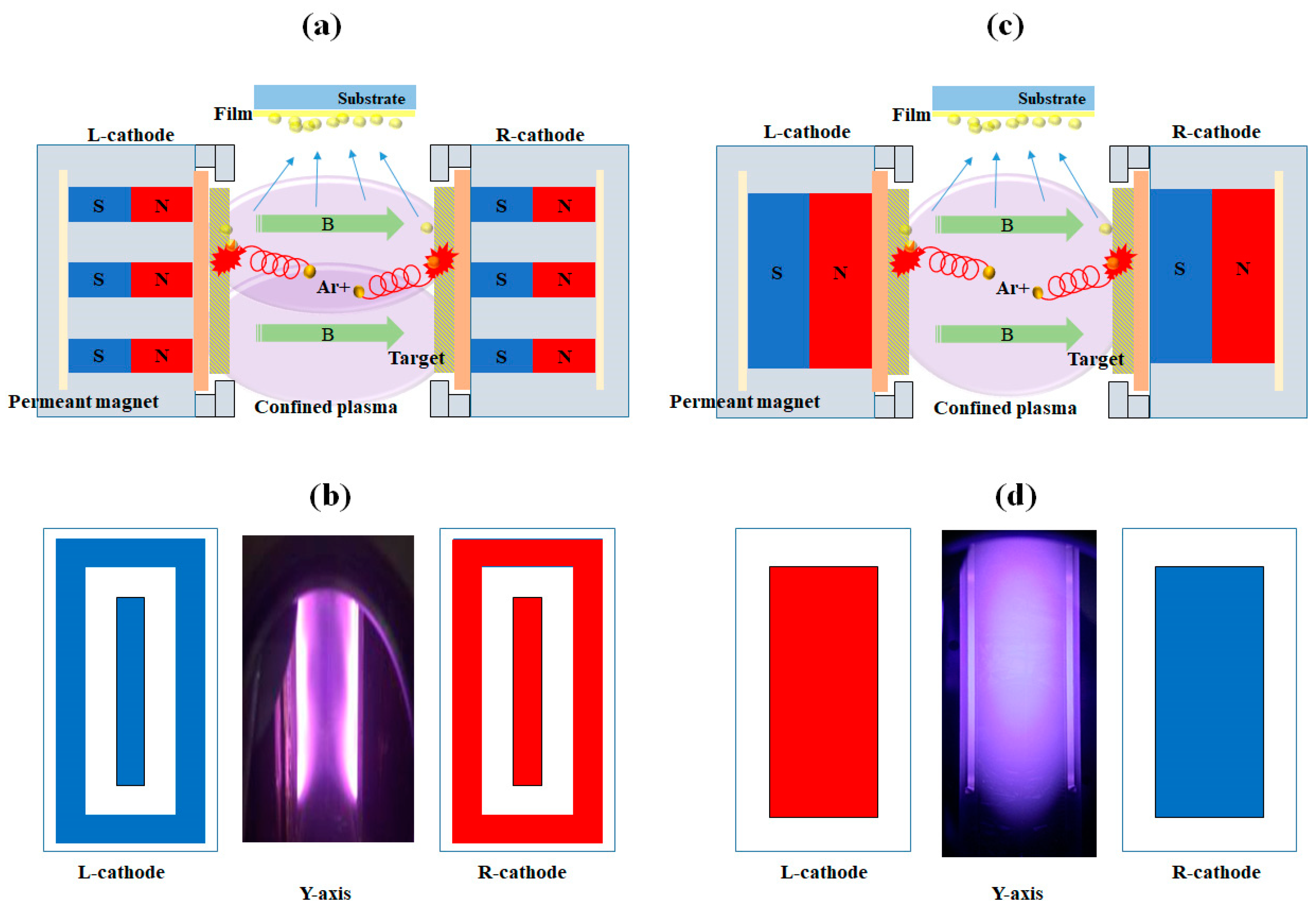
2. Experimental Methods and Measurements

All sputtering processes were carried out under the following conditions. Before sputtering, the base pressure was maintained at the high vacuum of 5.0 × 10⁻⁶ Torr using a turbo-molecular pump and a rotary pump. A DC power supply (MDX Magnetron delta 5kW, Advanced Energy Industries, Fort Collins, CO, USA) is employed as the sputtering power source.
More detailed films’ sputtering conditions are given in Table 1. To compare various permanent magnet arrangements inside the sputtering source, Indium Tin Oxide (ITO) targets were used for the discharge test and films were sputtered on the glass substrate. Soda-lime glass substrates were prepared after a standard cleaning process with Acetone, Ethanol, and D.I. water at the ultrasonication for 10 min. We designed two kinds of Open-type FTS (OFTS) and closed-type FTS (CFTS).
Two types of permanent magnetic arrangements were inserted into two cathodes, as shown Figure 1. Among common structural characteristics, they have two cathodes with opposite magnetic poles and plasma is generated between two targets. Then, a substrate is placed at the center of two targets. The working gas is mixed with argon and oxygen. Although the current FTS has better characteristics than those of DC magnetron sputtering, we still need better-deposited thin films, which can be used for higher-density magnetic recording media and other applications [17,18,19]. The main disadvantages of current FTS techniques is that magnetic fields are not applied perfectly perpendicularly to both of the targets, as shown in Figure 1. Therefore, the substrate is exposed to leaked magnetic fields, which may lead to the films on the substrate being damaged by plasma during deposition. To solve this problem, it is necessary to generate uniform magnetic fields by using a unique arrangement of magnets [20].
The surface morphology was measured via scanning probes microscopy (SPM, Park Systems XE-150, Suwon, Korea) at Smart Materials Research Center for IoT in Gachon University. The crystallographic structural properties of the samples were measured via X-ray diffraction (XRD, RINT2100, Rigaku Corporation, Tokyo, Japan) using Cu-Kα radiation (λ = 0.154056 nm, 40 kV, 40 mA) in the 2-theta scan mode. Electrical properties of the films were examined using a four-point probe (CMT-Series, Chang Min Tech. Corporation, Chatsworth, CA, USA). Magnetic flux density was measured using a gauss meter (MG-3002, Lutron Co.) and optical transmittance was measured using a UV-Vis spectrometer (LAMBDA750, PerkinElmer, Shelton, CT, USA).

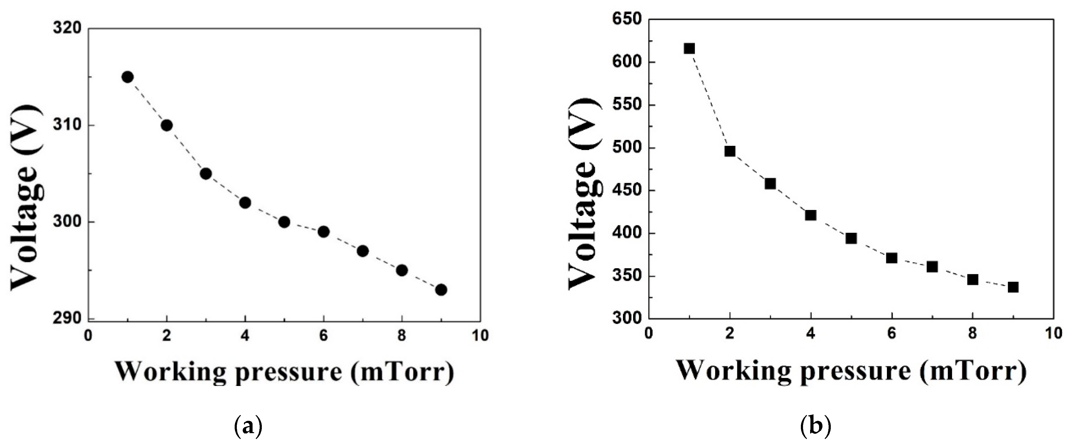
3. Results and Discussion

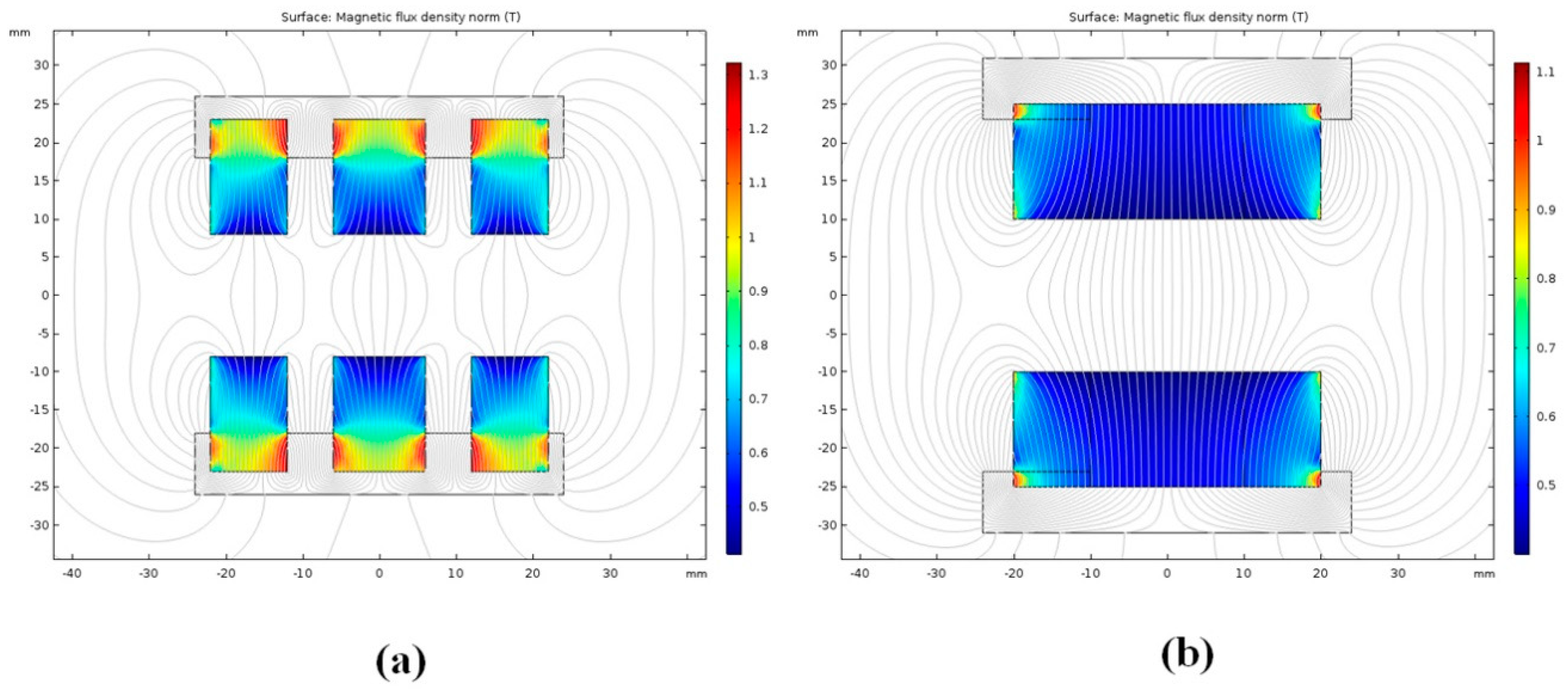
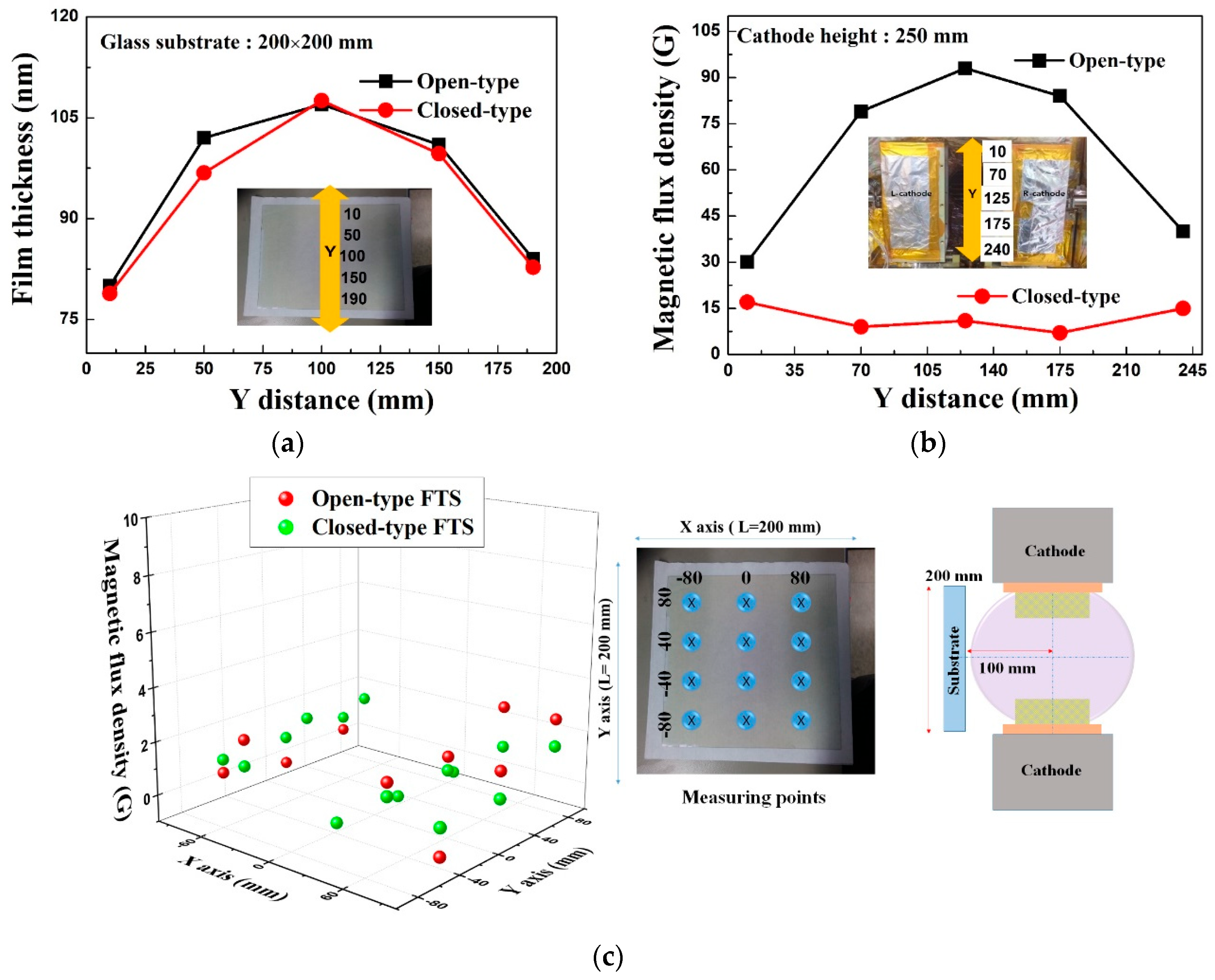
3.1. Magnetism Simulation

Before the preparation of magnetic arrangements, we performed magnetism simulation using the COMSOL Multiphysics software to obtain a prediction plasma similar to that generated in FTS systems.
In the initial discharge for film sputtering, electrons were generated from the surface of the target (or cathode) using a DC power supply and accelerated toward the anode (substrate or another target). Along the way to the anode, the electrons collided with other ions, which, thereby, increased the neutral background gas and the number of electrons. Simultaneously, the charged particles move in the radial direction of the magnetic field due to a Lorenzo force. Furthermore, the electric field intensity (E) induces the electrons to accelerate toward the anode with substantially high energy. Accelerated high energy atoms transfer their energy to bonded electrons within ions and neutral atoms. Thus, more atoms are ionized, and cations and anions are produced. Moreover, the atoms and ions are confined in discharged plasma generated above the target.

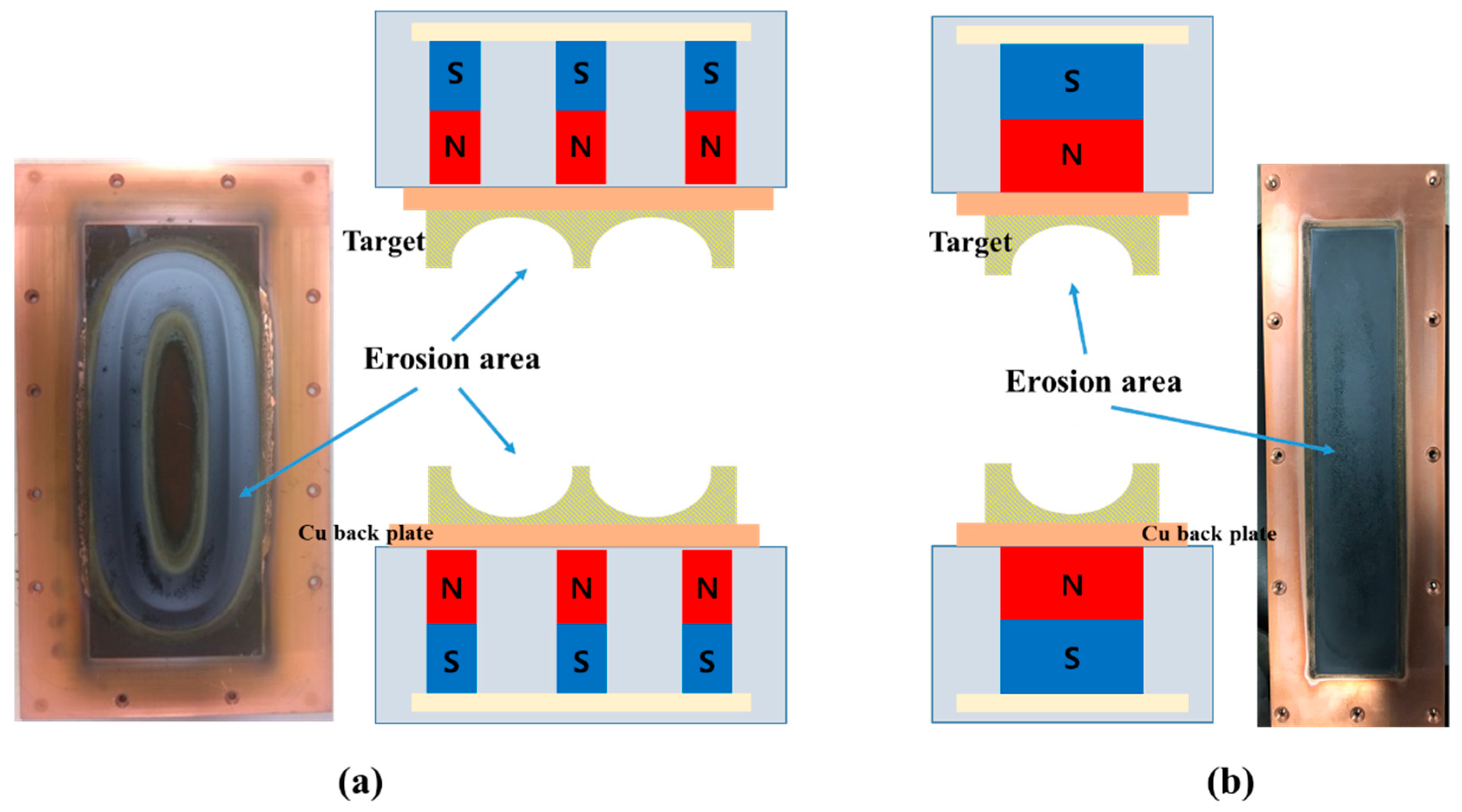
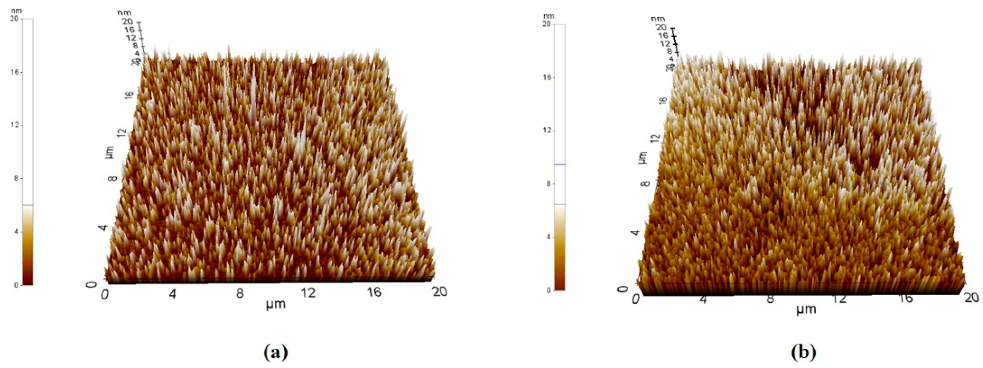
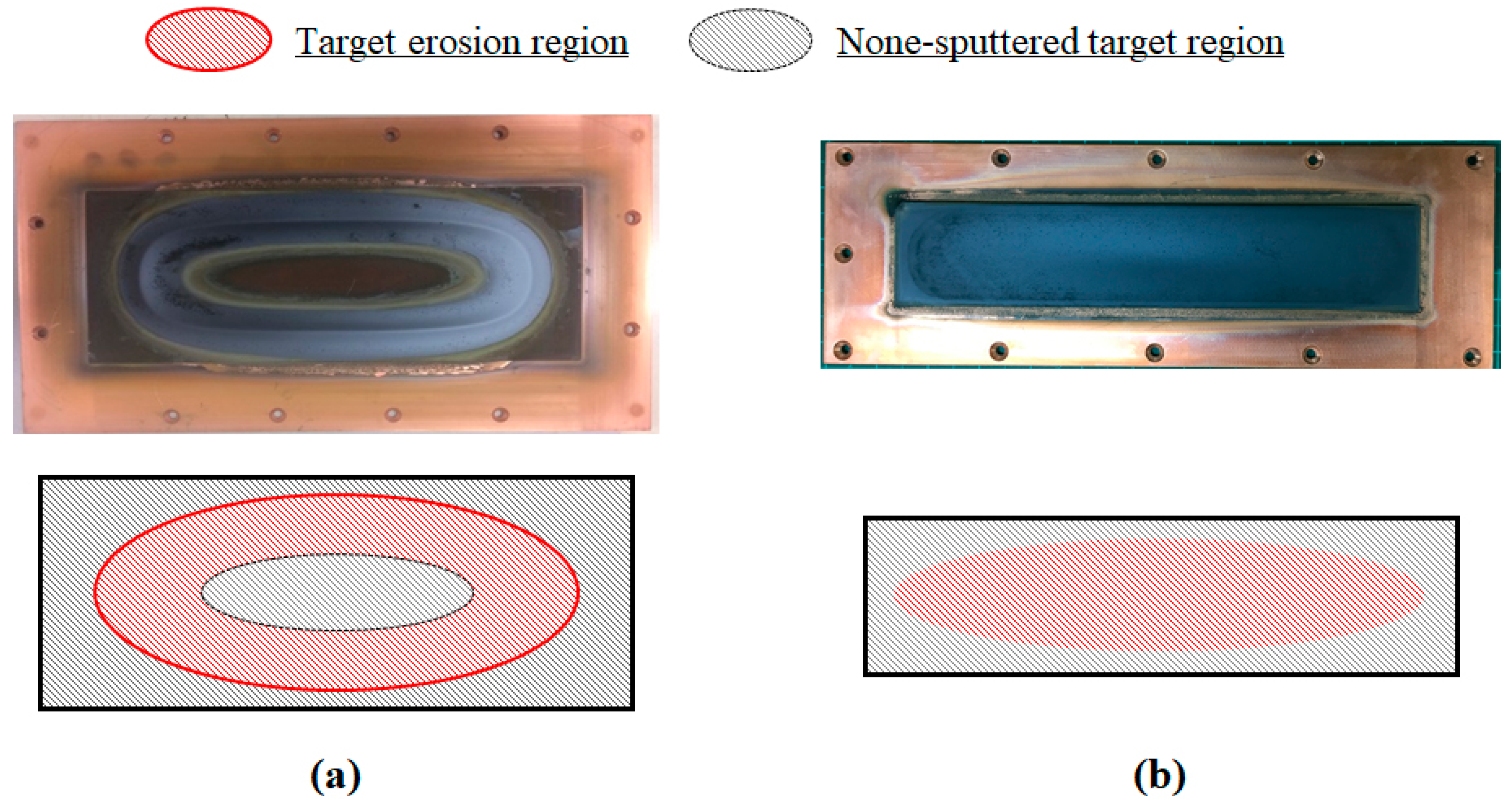
3.2. Film Uniformity and Target Erosion

The permanent magnet is placed behind the target/Cu back plate and generates a magnetic field through the plate. Figure 2 shows the magnet simulation results, and the lines represent the 2D orientation of the magnetic field that was generated from the permanent magnet. The cross-section of the magnet is separately shown in Figure 2a,b. The parts attached to both ends of the magnet is the york (previously referred to as the plate) that is held in position and prevents the magnetic field from permeating into its backside.
In Figure 2a, an open-type exhibits three magnetic field circular loops and the generated plasma was induced to be divided into three parts. However, a closed-type has only one magnetic field loop, and it the plasma can be confined in the space between the targets, as shown in Figure 1c,d along with the magnetic field. Thus, the magnetism simulation results show that the plasma can be confined in the space between the targets using the magnetic field generated by the permanent magnet (Ne-Fe-B) set behind each target.
In Figure 3, the distribution of magnetic flux density as a function of the arrangement of permanent magnets in the cathode is illustrated. The magnetic flux density was measured at five points between the two targets. The film was deposited on the glass substrate (200 mm × 200 mm) at a target thickness of 100 nm. The Nd-Fe-B magnet employed in this study has a maximum surface flux density of approximately 1321G. However, the sputtering source consists of a target, shield ring, and housing (stainless materials). Therefore, the magnet flux density decreased after all parts were fully assembled. Compared to CFTS, OFTS exhibits a higher magnet flux density, as shown in Figure 3a. However, film uniformity is consistent across all systems (Figure 3b). The film growth of the sputtered target is related to the outer region of the magnetic field. Even upon a 50% reduction of the size of the target and magnet, the same films’ uniformity can be obtained on the substrate.
Furthermore, during sputtering, a target erosion area is formed along with a magnetic field. Target materials sputtered from the target erosion area are displaced toward the substrate and grow on the substrate with a high energy. Therefore, a large target erosion can achieved by optimally designing the magnet arrays and controlling the incidence of plasma on the target.
We observed the condition of the ITO film subsequent to sputtering, and the photograph was obtained, as shown in Figure 3. Moreover, we measured the magnetic field strength on the surface of the substrate between the two targets. After the substrate was mounted on the substrate holder in the chamber, as shown in Figure 1, we measured the magnetic field density on the surface of the substrate from the outside using a Gauss meter. The magnetic field density was approximately zero regardless of the type of sputtering, as shown in Figure 3c. This means that a magnetic field loop was generated around the cathode and the anode where the plasma was confined between the two targets.
In the OFTS system, a two-part erosion was formed on the ITO target. However, in the CFTS system, a one-part erosion was formed. This could also be anticipated from the magnetism simulation results (Figure 2). The OFTS system exhibits magnetic flux circuits induced by each permanent magnet. In the regions where the loops overlapped, particles with high energy exhibited increased bombardment with the targets compared to the bombardment in the other regions. Furthermore, we confirmed that such sputtering could be employed to prepare films regardless of the target size, as shown in Figure 4. Moreover, we calculated the usage of the sputter targets by using the target erosion ratio equation, as follows.
Target erosion ratio (%) = [(Erosion target area)/(Total target area)] × 100
Figure 5 shows the eroded region in the surface of the target after sputtering. Using the equation, the target erosion ratio of the OFTS system is determined to be 53% and that of CFTS is 70%. The target material consumption decreased when the arrangement of the magnets was changed from open-type to closed-type for sputtering using the same film. It is suggested that enhancing the flux densities at the target surface enhance the sputtering efficiency by as much as 50%.

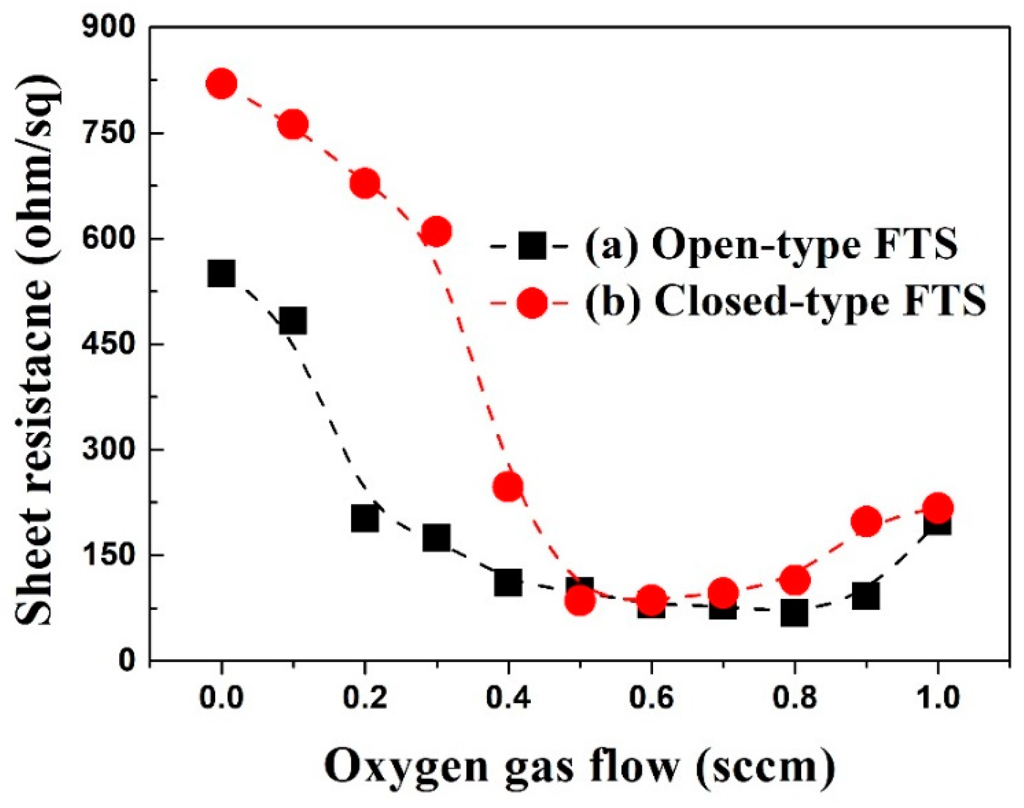
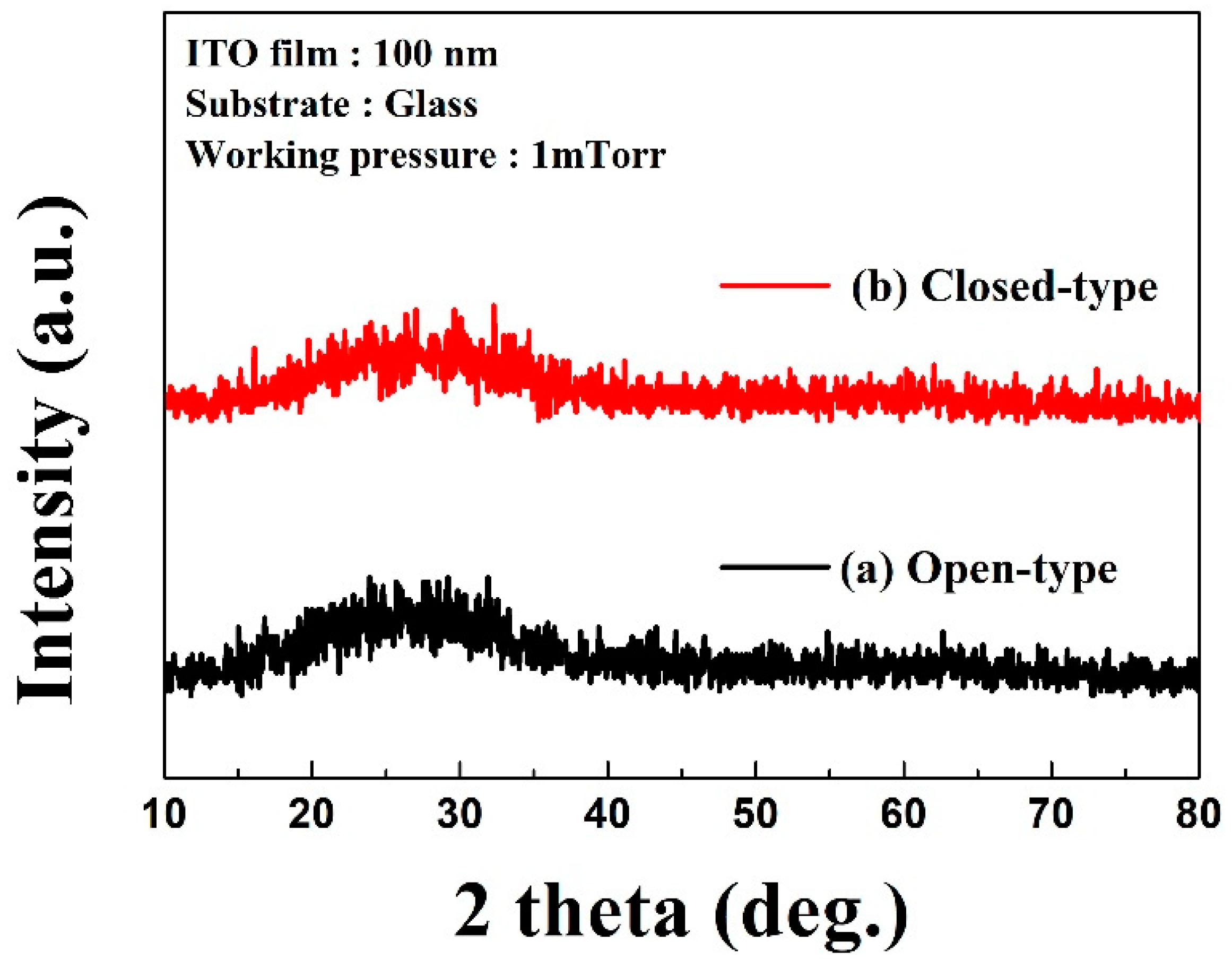
3.3. Properties of Films

Figure 6 shows the discharge characteristics with respect to working pressure for sputtering at a fixed 500 W using the FTS system. The typical discharge properties of magnetron sputtering are well-known to be dependent on the discharge voltage and the current of the cathode, working pressure, magnetic flux density, and input power [21,22].
In a normal sputtering system, the anode is perpendicular to the target, such as the cathode. However, in the FTS system configuration, two targets are connected in series with the power supply, and these act as the cathode. The anode is dark shielding and substrate. In the plasma, the number of Ar/Ar+ atoms/ions and electrons were increased, and film sputtering enabled the growth of the substrate at a relatively low working pressure (~1 mTorr). Therefore, it is crucial for the film in the sputtering process. We investigated the relationship between the voltage and working pressure, and the results are summarized in Figure 6.
At a constant input power, with a changing working pressure in the chamber, the current (I) and voltage (V) are as follows:
P = (△I) × (△V)
where △I is the variation value in the current, △V is the variation in the voltage, and P is the input power. Regardless of the magnetic arrays used, the voltage was observed to decrease as operating pressure increased. The initial voltage of CFTS, which exhibits a higher magnetic flux density than OFTS, is approximately 620 V (80.1 mA).
The initial voltage of CFTS was approximately 315 V, and its initial current decreased from a maximum of 158.7 mA as the functions of working pressure. Therefore, in the case of the OFTS configuration, the cathode currents were observed to be higher than those in the case of CFTS under a similar working pressure and input power. It has been reported that the magnetic field in FTS enables controlling the confinement of plasma as well as a lower voltage and higher current at a low working pressure, in contrast to conventional magnetrons at low pressures.
The XRD patterns of the prepared ITO films are shown in Figure 7. From the XRD patterns, it can be observed that the crystal quality of ITO where the film is grown at a working pressure of 1 mTorr without substrate heating is almost amorphous even though two kinds of magnetic armaments were installed in the sputtering source. In the sputtering process, the crystallization of films is affected by the film thickness and substrate temperature [23,24,25]. In conventional magnetron sputtering, the kinetic energies of sputtered particles and other energetic particles (Ar and O-) cause an increase in the substrate temperature and enhance the crystallinity of the films during the surface migration, as numerous particles arrive at the substrate. Therefore, ITO films with a polycrystalline structure can be grown using magnetron sputtering at room temperature [24,25,26]. However, Shigesato et al. [27] reported that ITO films with a thickness of 170 nm exhibited film growth with the crystallization of the (400) plane and that polycrystalline ITO was grown on a glass substrate at a thickness of approximately 240 nm. Moreover, in contrast with conventional magnetron sputtering systems, particles with a lower kinetic energy that impact less plasma damage are produced in the FTS system [27,28]. Consequently, the internal damage caused by particle bombardment during the film growth is substantially reduced.
In the case of the FTS system, phenomena as similar to those mentioned above were observed in this study as well. No crystal peak could be observed in the XRD pattern due to ITO film being 100-nm thick. Moreover, its substrate was located outside the high-density plasma region. The increase in substrate temperature was relatively low during the sputtering process. The relatively low temperature could contribute to be the final ITO film being amorphous [29,30].
To investigate the effect of temperature on the sputtering, we employed a thermos label tap (NiGK Corportion Company, 80–95 °C). For conventional DC sputtering, we used DC magnetron sputtering (ITO target size: 2 inch) in our laboratory. We observed the thermos label tape in the sputtering condition including 3 mTorr with Ar atmosphere and distance from the target to the substrate (DT-S) at 100 mm. The substrate temperature is shown in Figure 8. Before the substrates were loaded onto the holder in the chamber, the tape was attached behind the substrate, and the color change of the tapes was observed. Figure 8 shows the images in which reversed dark-black colored spots can be observed after and before sputtering for 1 h. The substrate temperature increased to at least 80 °C even though film sputtering was successfully completed. In contrast with normal DC magnetron sputtering, no color change was observed in the tape in the case of all types of FTS systems. Therefore, it is thought that FTS could be employed to prepare films at a low temperature with low damage.
According to previous results obtained by another group of using magnetron sputtering, ITO films could be made to exhibit improved electrical properties by adding a small amount of oxygen gas to the pure argon gas atmosphere during sputtering. We investigated the effect of oxygen gas flow on the electrical properties of ITO films, and sheet resistance was measured with respect to an increase in the oxygen amount in the Ar working gas atmosphere, as shown in Figure 9. At oxygen flow rates of 0 to 1.0 sccm, the ITO film (100 nm) exhibited a sheet resistance of 550 ohm/sq in the case of OFTS and 820 ohm/sq in the case of CFTS. With an increasing amount of oxygen gas, sheet resistance of the films decreased from 820 to 85.53 ohm/sq (CFTS) and from 550 to 67.42 ohm/sq (OFTS).
It is known that the electrical properties of ITO films depend on free carriers, a strong scattering center, and oxygen vacancies. The increase in sheet resistance was due to the decrease of the carrier mobility [31]. The mobility was improved due to an increasing oxygen flow rate during sputtering, even though carrier concentration decreased [32,33]. The enhancement of sheet resistance may be attributed to the formation of SnO2 in the ITO films, which results in the decrease of oxygen vacancies in the films, as the electrons that are released due to the substitution enter Sn atoms in the sublattice and form doubly charged oxygen vacancies [26]. Meng [34] reported that a high insertion of oxygen gas could damage the grown film and substrate as a result of an increase in the plasma bombardment energy during film sputtering and changes in the film deposition rate in the conventional magnetron sputtering system.
However, based on XRD patterns (Figure 7) and sheet resistance of ITO films (Figure 9), all ITO films, grown in the OFTS and CFTS, have no crystal peak and we confirmed that the oxygen gas is more effective when enhancing the electrical properties of ITO films using less than 5% of oxygen gas in an Ar/O2 mixture.
The spectral transmittance of the ITO films was obtained by scanning the films from 340 nm to 800 nm and is illustrated in Figure 10. All ITO films on the glass substrate deposited under different oxygen flow rates exhibit transmittance of more than 85% at the wavelength of approximately 550 nm except for the samples prepared without oxygen gas. With an increasing oxygen flow, the transmittance attains a maximum value of 95% for the wavelength of 550 nm. Gupta et al. [35] reported that the absorption edge is moved to higher energies (referred to as blue shift or Burstein-Moss (BM)) as a result of the high charge carrier concentration of ITO films as arising from an increase in the oxygen gas flow. Moreover, although the BM phenomenon could be one of the reasons for the blue shift of the absorption edge is the high charge carrier concentration. Therefore, the charge carrier concentration of these samples should increase with an rise in the oxygen gas flow rate [36,37].
The roughness of each surface was observed using SPM, as shown in Figure 11. More detailed values of the surface roughness are shown in Table 2. The surface roughness (RMS) of the ITO film prepared via OFTS, from 1.565 to 2.006 nm, is shown in Figure 11a,b. The Ra (roughness average) value of the film also slightly increased from 2.151 to 2.575 nm. Using AFM, we confirmed that ITO films have the smoothened surface regardless of the magnetic type.

4. Conclusions

It is well known that the FTS system possesses an off-axis substrate-target geometry in contrast with traditional magnetron sputtering with an on-axis geometry in which the substrate faces the target. We investigated the effect of the magnet arrangement inside the cathode of the FTS system on the sputtering outcome. Prior to analyzing the magnetic array and performing sputtering, we predicted plasma confinement on the target surface using the result of a magnetism simulation. We selected two kinds of sputtering systems known as OFTS and CFTS, and inserted two cathodes in the systems. In the optimized conditions of sputtering, the obtained films (thickness: 100 nm) exhibited optical transmittance up to 85% in the visible range and approximately 67 ohm/sq without heating. Moreover, a maximum target erosion of 70% was observed, and it is considered that this could enhance the sputtering efficiency by as much as 50% if the target size is reduced to half the original size of the target. The substrate temperature was relatively low compared to that exhibited by conventional magnetron sputtering even though film sputtering was successfully achieved.

Author Contributions

S.K.; Writing-review and Original draft preparation. K.H.K. Reviewing and editing. All authors have read and agreed to the published version of the manuscript.

Funding

Gachon University research fund of 2019 (GCU-2019-0302) and Basic Science Research Capacity Enhancement Project through Korea Basic Science Institute (National research Facilities and Equipment Center) grant funded by the Ministry of Education (Grant No. 2019R1A6C1010016).

Conflicts of Interest

The authors declare no conflicts of interest.

References

  1. Pereira, P.J.S.; Escrivão, M.L.; Teixeira, M.R.; Maneira, M.J.P.; Nunes, Y. Analytical model and measurements of the target erosion depth profile of balanced and unbalanced planar magnetron cathodes. Plasma Sources Sci. Technol. 2014, 23. [Google Scholar] [CrossRef]
  2. Hou, Q.; Buckeridge, J.; Lazauskas, T.; Mora-Fonz, D.; Sokol, A.A.; Woodley, S.M.; Catlow, C.R.A. Defect formation in In2O3 and SnO2: A new atomistic approach based on accurate lattice energies. J. Mater. Chem. C 2018, 6, 12386–12395. [Google Scholar] [CrossRef] [Green Version]
  3. Tien, C.-L.; Lin, H.-Y.; Chang, C.-K.; Tang, C.-J. Effect of Oxygen Flow Rate on the Optical, Electrical, and Mechanical Properties of DC Sputtering ITO Thin Films. Adv. Condens. Matter Phys. 2018, 2018. [Google Scholar] [CrossRef] [Green Version]
  4. Shin, H.-S.; Seo, K.-W.; Lee, J.-H.; Kim, H.-K. Effect of Target–Substrate Distance on the Properties of Hetero Facing Target Sputtered Al-Ga-Zn-O Films. Jpn. J. Appl. Phys. 2013, 52. [Google Scholar] [CrossRef] [Green Version]
  5. Xiao, Y.; Gao, F.; Dong, G.; Guo, T.; Liu, Q.; Ye, D.; Diao, X. Amorphous indium tin oxide films deposited on flexible substrates by facing target sputtering at room temperature. Thin Solid Films 2014, 556, 155–159. [Google Scholar] [CrossRef]
  6. Kadokura, S.; Naoe, M.; Nakagawa, S. Nano-size Magnetic Crystallite Formation in Go-Cr Thin Films for Perpendicular Recording Media. IEEE Trans. Magn. 1998, 34, 1642–1644. [Google Scholar] [CrossRef]
  7. Noda, K.; Kadokura, S.; Naoe, M. Microstructure and noise characteristics of Co-Cr-Ta films on ultraflat glass substrates for longitudinal recording disks. J. Appl. Phys. 2000, 87, 6343–6345. [Google Scholar] [CrossRef]
  8. Matsushita, N.; Nakagawa, S.; Naoe, M. Preparation of Co ferrite thin films with large perpendicular and in-plane coercivities by facing targets sputtering. IEEE Trans. Magn. 1992, 28, 3108–3110. [Google Scholar] [CrossRef]
  9. Kim, H.-K.; Kim, S.W.; Lee, K.-S.; Kim, K.H. Direct Al cathode layer sputtering on LiF@Alq3 using facing target sputtering with a mixture of Ar and Kr. Appl. Phys. Lett. 2006, 88. [Google Scholar] [CrossRef]
  10. Fan, Q.H.; Chen, H.Y. Effects of magnetic field on the target erosion in the symmetrical magnets magnetron sputtering method. Thin Solid Films 1993, 229, 143–145. [Google Scholar] [CrossRef]
  11. Liu, C.-T.; Lai, M.-C.; Hwang, C.-C.; Tu, C.-H.; Liu, L.-Y.; Hsu, Y.-W. Enhancements of Substrate Deposition Rate and Target Erosion Profile in a DC Magnetron Sputtering System. IEEE Trans. Magn. 2009, 45, 4391–4394. [Google Scholar] [CrossRef]
  12. Lin, C.; Sun, D.C.; Ming, S.L.; Jiang, E.Y.; Liu, Y.G. Magnetron facing target sputtering system for fabricating single-crystal films. Thin Solid Films 1996, 279, 49–52. [Google Scholar] [CrossRef]
  13. Shin, H.-S.; Lee, J.-H.; Kwak, J.-S.; Lee, H.-H.; Kim, H.-K. Linear facing target sputtering of the epitaxial Ga-doped ZnO transparent contact layer on GaN-based light-emitting diodes. J. Phys. D Appl. Phys. 2013, 46, 1–6. [Google Scholar] [CrossRef]
  14. Murphy, M.J.; Cameron, D.C.; Karim, M.Z.; Hashmi, M.S.J. Magnetic fields in magnetron sputtering systems. Surf. Coat. Technol. 1993, 57, 1–5. [Google Scholar] [CrossRef]
  15. Hollerweger, R.; Holec, D.; Paulitsch, J.; Rachbauer, R.; Polcik, P.; Mayrhofer, P.H. Magnetic field strength influence on the reactive magnetron sputter deposition of Ta2O5. J. Phys. D Appl. Phys. 2013, 46. [Google Scholar] [CrossRef] [Green Version]
  16. Noda, K.; Hirata, T.; Takashi, K.; Naoe, M. Novel facing targets sputtering apparatus with uniform magnetic field and plasma-free substrates. Vacuum 1998, 51, 687–690. [Google Scholar] [CrossRef]
  17. Hoshi, Y.; Naoe, M.; Yamanka, S. High Rate Deposition of Iron Films by Sputtering from Two Facing Targets. Jpn. J. Appl. Phys. 1977, 16, 1715–1716. [Google Scholar] [CrossRef]
  18. Kageyama, J.; Yoshimoto, M.; Matsuda, A.; Akao, Y.; Shidojim, E. Numerical simulation of plasma confinement in DC magnetron sputtering under different magnetic fields and anode structures. Jpn. J. Appl. Phys. 2014, 53. [Google Scholar] [CrossRef]
  19. Guo, T.; Dong, G.; Liu, Q.; Wang, M.; Wang, M.; Gao, F.; Chen, Q.; Yan, H.; Diao, X. Optimization of oxygen and pressure of ZnO: Al films deposited on PMMA substrates by facing target sputtering. Superlattices Microstruct. 2013, 64, 552–562. [Google Scholar] [CrossRef]
  20. Kim, H.-K.; Moon, J.-M. Sputtering of Aluminum Cathodes on OLEDs Using Linear Facing Target Sputtering with Ladder-Type Magnet Arrays. J. Electrochem. Soc. 2008, 155, J187–J192. [Google Scholar] [CrossRef]
  21. Liebrerman, M.A.; Lichtenberg, A.J. Principles of Plasma Discharges and Materials Processing, 2nd ed.; John Wiley & Sons Inc.: Hoboken, NJ, USA, 2005. [Google Scholar]
  22. Westwood, W.D.; Maniv, S.; Scanlon, P.J. The current-voltage characteristic of magnetron sputtering systems. J. Appl. Phys. 1983, 54, 6841–6846. [Google Scholar] [CrossRef]
  23. Ghorannevis, Z.; Akbarnejad, E.; Ghoranneviss, M. Structural and morphological properties of ITO thin films grown by magnetron sputtering. J. Theor. Appl. Phys. 2015, 9, 285–290. [Google Scholar] [CrossRef] [Green Version]
  24. Morikawa, H.; Fujita, M. Crystallization and decrease in resistivity on heat treatment of amorphous indium tin oxide thin films prepared by dc magnetron sputtering. Thin Solid Films 1999, 339, 309–313. [Google Scholar] [CrossRef]
  25. Shigesato, Y.; Panie, D.C. A microstructural study of low resistivity tin-doped indium oxide prepared by dc magnetron sputtering. Thin Solid Films 1994, 238, 44–50. [Google Scholar] [CrossRef]
  26. Hosono, H.; Ueda, K. Transparent Conductive Oxides. In Springer Handbook of Electronic and Photonic Materials, 2nd ed.; Kasap, S., Capper, P., Eds.; Springer: New York, NY, USA, 2017; pp. 1391–1403. [Google Scholar]
  27. Shigesato, Y.; Koshi-ishi, R.; Kawashima, T.; Ohsako, J. Early stages of ITO deposition on glass or polymer substrates. Vacuum 2000, 59, 614–621. [Google Scholar] [CrossRef]
  28. Lines, V.; Bivour, M.; Iwata, H.; Ortner, K. Comparison of low damage sputter deposition techniques to enable the application of very thin a-Si passivation films. AIP Conf. Proc. 2019, 2147. [Google Scholar] [CrossRef]
  29. Song, P.K.; Akao, H.; Kamei, M.; Shigesato, Y.; Yasui, I. Preparation and Crystallization of Tin-doped and Undoped Amorphous Indium Oxide Films Deposited by Sputtering. Jpn. J. Appl. Phys. 1999, 38, 5224–5226. [Google Scholar] [CrossRef]
  30. Ahmed, N.M.; Sabah, F.A.; Abdulgafour, H.I.; Alsadig, A.; Sulieman, A.; Alkhoaryef, M. The effect of post annealing temperature on grain size of indium-tin-oxide for optical and electrical properties improvement. Results Phys. 2019, 13. [Google Scholar] [CrossRef]
  31. Chen, A.; Zhu, K.; Zhong, H.; Shao, Q.; Ge, G. A new investigation of oxygen flow influence on ITO thin films by magnetron sputtering. Sol. Energy Mater. Sol. Cells 2014, 120, 157–162. [Google Scholar] [CrossRef] [Green Version]
  32. Li, S.; Qiao, X.; Chen, J. Effects of oxygen flow on the properties of indium tin oxide films. Mater. Chem. Phys. 2006, 98, 144–147. [Google Scholar] [CrossRef]
  33. Tahar, R.B.H.; Ban, T.; Ohya, Y.; Takahashi, Y. Tin doped indium oxide thin films: Electrical properties. J. Appl. Phys. 1998, 83, 2631–2645. [Google Scholar] [CrossRef]
  34. Meng, L.-J.; Maçarico, A.; Martins, R. Study of annealed indium tin oxide films prepared by rf reactive magnetron sputtering. Vacuum 1995, 6, 673–680. [Google Scholar] [CrossRef]
  35. Gupta, L.; Mansingh, A.; Srivastava, P.K. Band GAP Narrowing and the band structure of tindoped indium oxide films. Thin Solid Films 1989, 176, 33–44. [Google Scholar] [CrossRef]
  36. Cho, S.H.; Park, J.H.; Lee, S.C.; Cho, W.S.; Lee, J.H.; Yon, H.H.; Song, P.K. Effects of O2 addition on microstructure and electrical property for ITO films deposited with several kinds of ITO targets. J. Phys. Chem. Solids 2008, 69, 1334–1337. [Google Scholar] [CrossRef]
  37. Kim, C.E.; Moon, P.; Kim, S.; Myoung, J.-M.; Jang, H.W.; Bang, J.; Yun, I. Effect of carrier concentration on optical bandgap shift in ZnO: Ga thin films. Thin Solid Films 2010, 518, 6304–6307. [Google Scholar] [CrossRef]
Figure 1. Schematic diagram of facing target sputtering (FTS) system with various magnet arrays. (a) and (b) Open-type FTS, (c) and (d) Closed-type FTS.
Coatings 10 00321 g001
Figure 2. 2-D magnetism simulation results of the magnetic field induced as a function of the arrangement of permanent magnets obtained using COMSOL Multiphysics software. (a) Open-type and (b) Closed-type.
Coatings 10 00321 g002
Figure 3. Distribution of magnetic flux density between two targets as a function of the arrangement of permanent magnets in cathode (Y: perpendicular direction). (a) Open-type Facing Targets Sputtering (FTS), (b) Closed-type FTS, and (c) magnetic flux density measured on the surface of the substrate.
Coatings 10 00321 g003
Figure 4. Photos of targets after sputtering and cross-sectional profiles of sputter target erosion. (a) Open-type FTS and (b) closed-type FTS.
Coatings 10 00321 g004
Figure 5. Photo images of the target erosion region for a target erosion ratio. (a) Open-type FTS (OFTS) and (b) Closed-type FTS (CFTS).
Coatings 10 00321 g005
Figure 6. Discharge voltage with respect to working pressure for (a) open-type FTS (OFTS) and (b) closed-type FTS (CFTS).
Coatings 10 00321 g006
Figure 7. X-ray diffraction patterns of prepared films at a working pressure of 1 mTorr without substrate heating. (a) Open-type FTS (OFTS) and (b) Closed-type FTS (CFTS).
Coatings 10 00321 g007
Figure 8. Color changes of the thermo label tape before and after sputtering. (a) Before sputtering, (b) After sputtering in DC magnetron, (c) After sputtering in OFTS, and (d) After sputtering in CFTS.
Coatings 10 00321 g008
Figure 9. Electrical properties of prepared films as a function of oxygen gas flow. (a) Open-type FTS (OFTS) and (b) Closed-type FTS (CFTS).
Coatings 10 00321 g009
Figure 10. Optical transmittance spectra of ITO thin films deposited under different oxygen flow rates. (a) Open-type FTS and (b) Closed-type FTS.
Coatings 10 00321 g010
Figure 11. Surface morphology of ITO film obtained via (a) open-type FTS and (b) closed-type FTS.
Coatings 10 00321 g011
Table 1. Comparison of detailed sputtering conditions by the magnet arrangement.
ParametersConditions
Open-Type FTS (OFTS)Closed-Type FTS (CFTS)
Target materialITO (In2O3: 90%, SnO2: 10%)
Target size250 × 100 mm250 × 50 mm
Base pressure5 × 10−6 Torr
Working pressure0.5–5 mTorr
Working gasAr: 9–10 sccm, O2: 0–1sccm
DC power (5kW)500 W
Distance from the target to the substrate
(DT-S)
100 mm
Distance from the target to the target
(DT-T)
100 mm
Film thickness100 nm
Table 2. Surface roughness values of prepared ITO films.
Magnetic TypeRa (nm)RMS (nm)
Open-type FTS(1)2.0062.575
Closed-type FTS(2)1.5652.151
Sputtering conditions: (1) Oxygen gas flow = 0.8 sccm and (2) Oxygen gas flow = 0.6 sccm.

