Electrical and Optical Properties of Amorphous SnO2:Ta Films, Prepared by DC and RF Magnetron Sputtering: A Systematic Study of the Influence of the Type of the Reactive Gas

Abstract
1. Introduction
2. Experimental
3. Results and Discussion
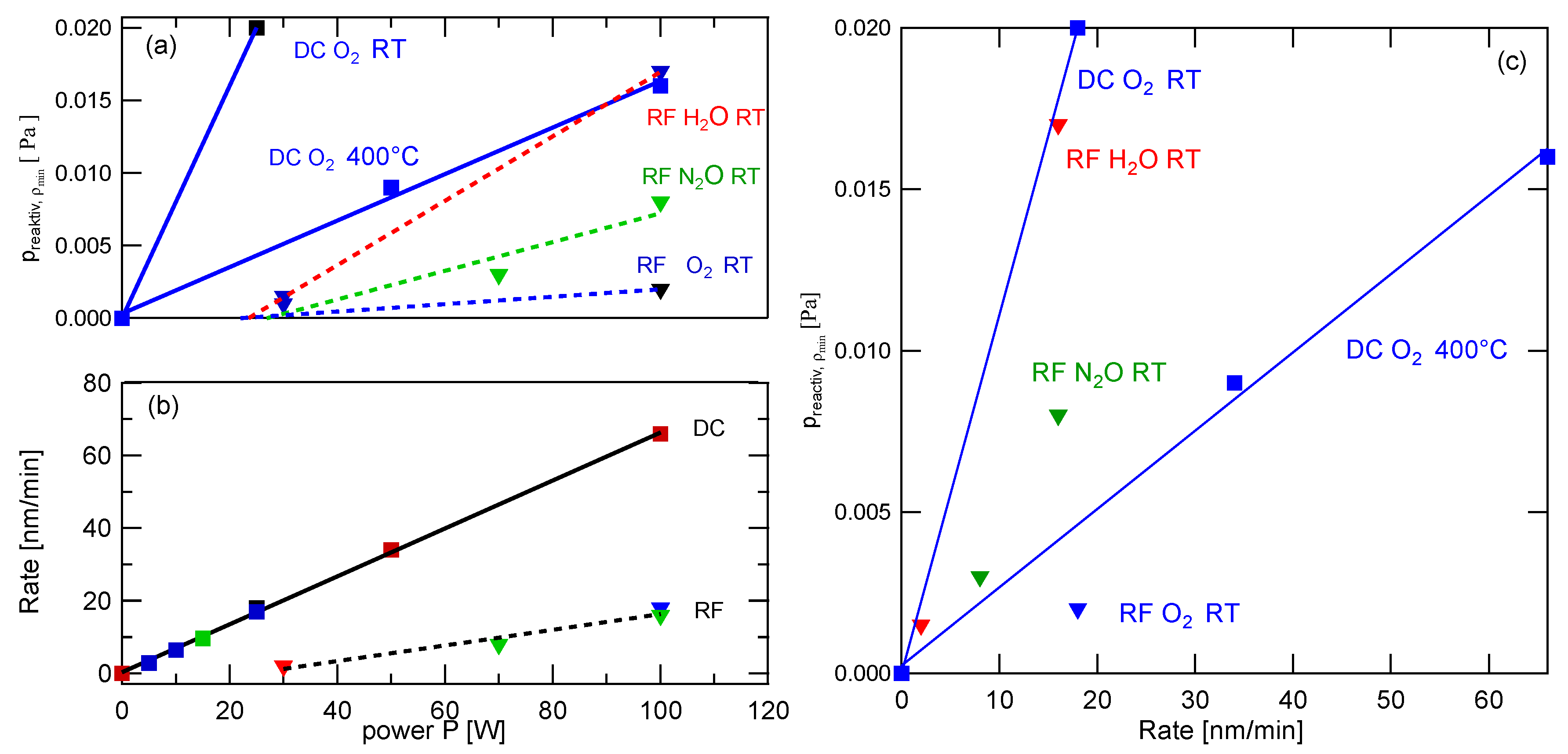
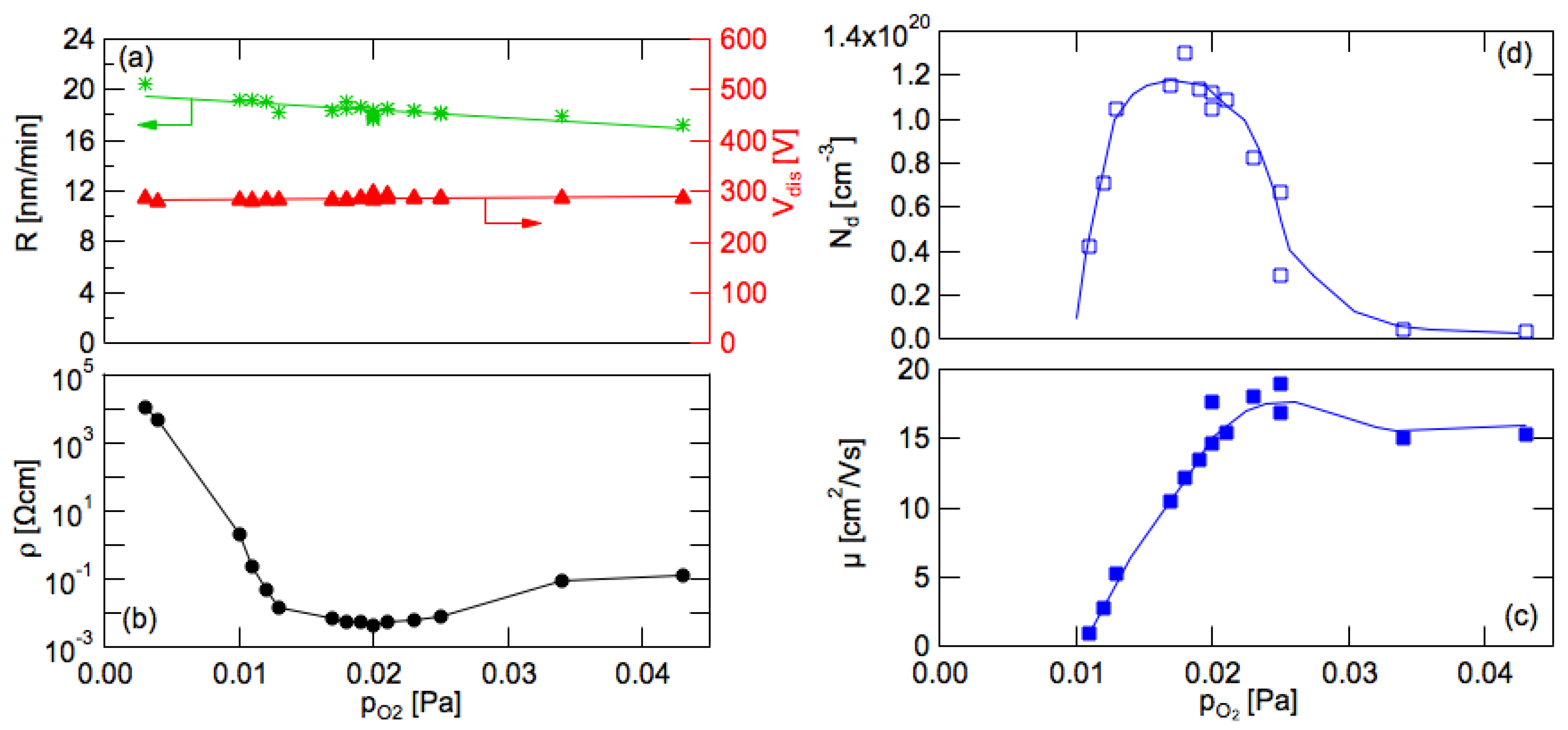
3.1. Deposition Characteristics
- The lower discharge voltages leading to lower sputtering yields;
- The fact that, in the RF case, the target is only at a sufficiently high negative potential every second half-wave, allowing an acceleration of positive Ar ions to the target surface [43].
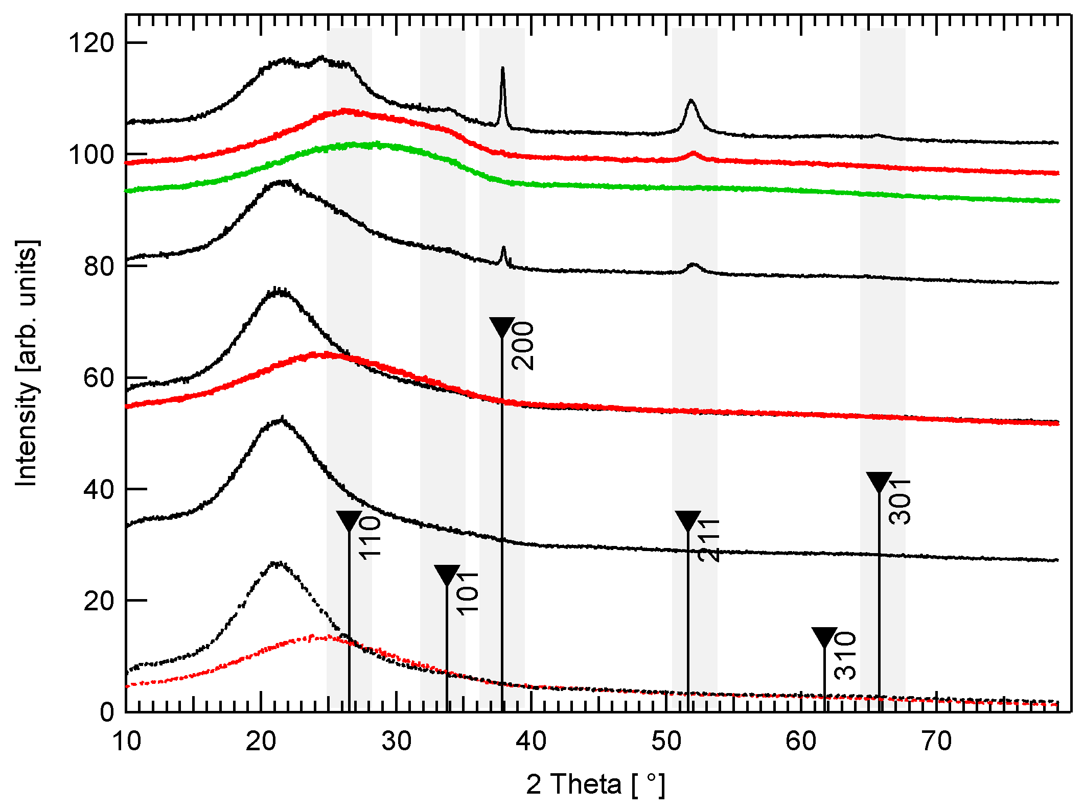
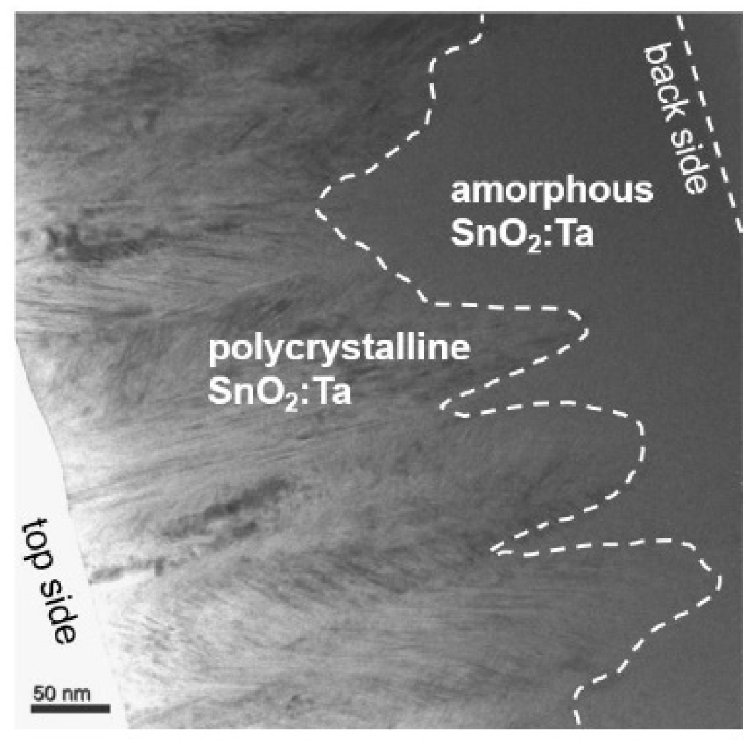
3.2. Phase Composition
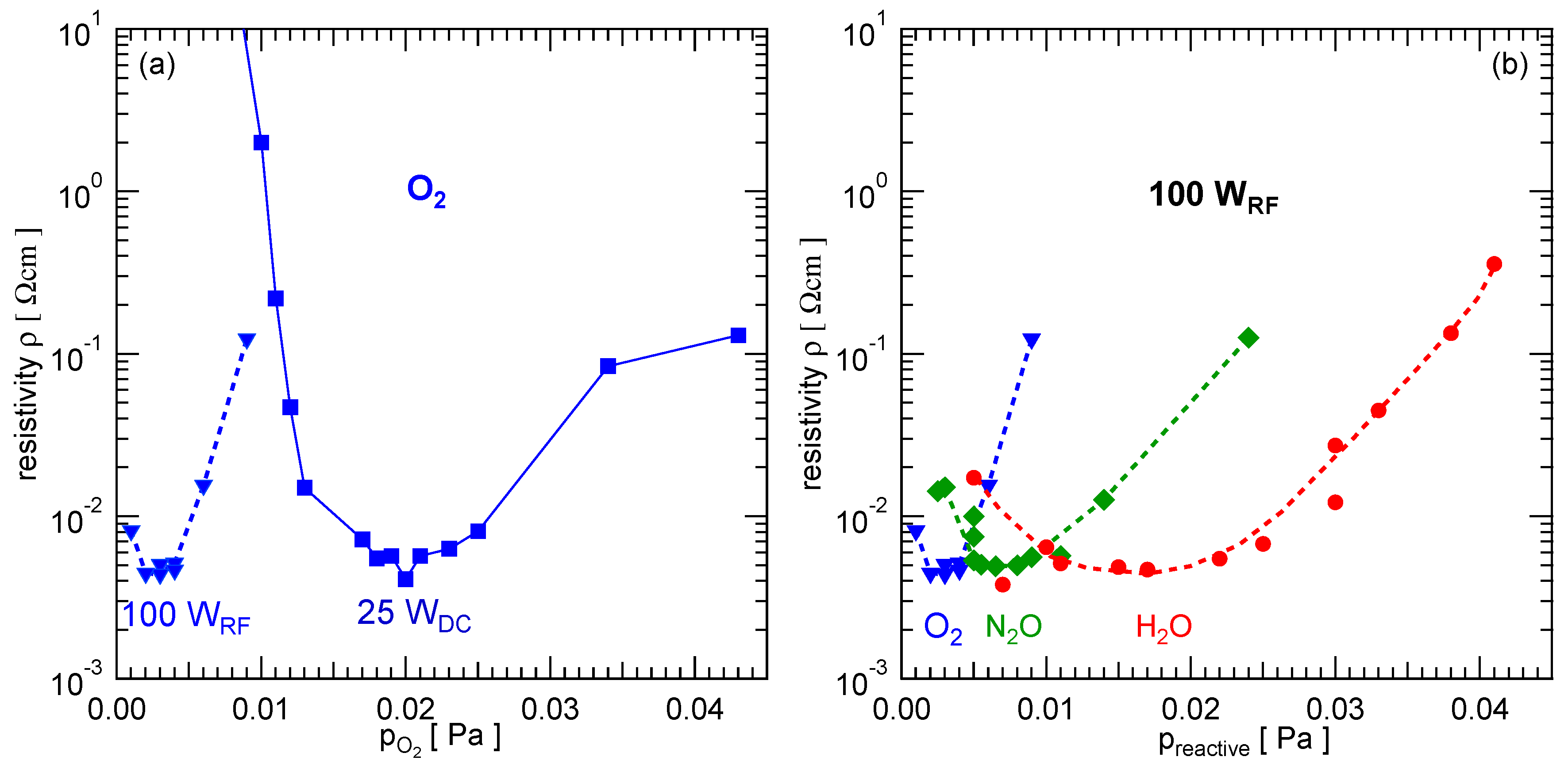
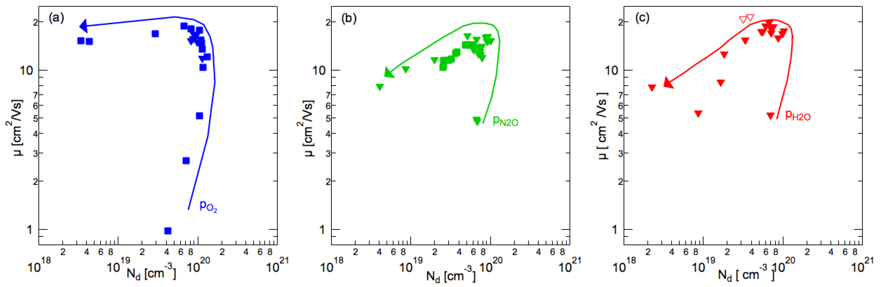
3.3. Resistivity
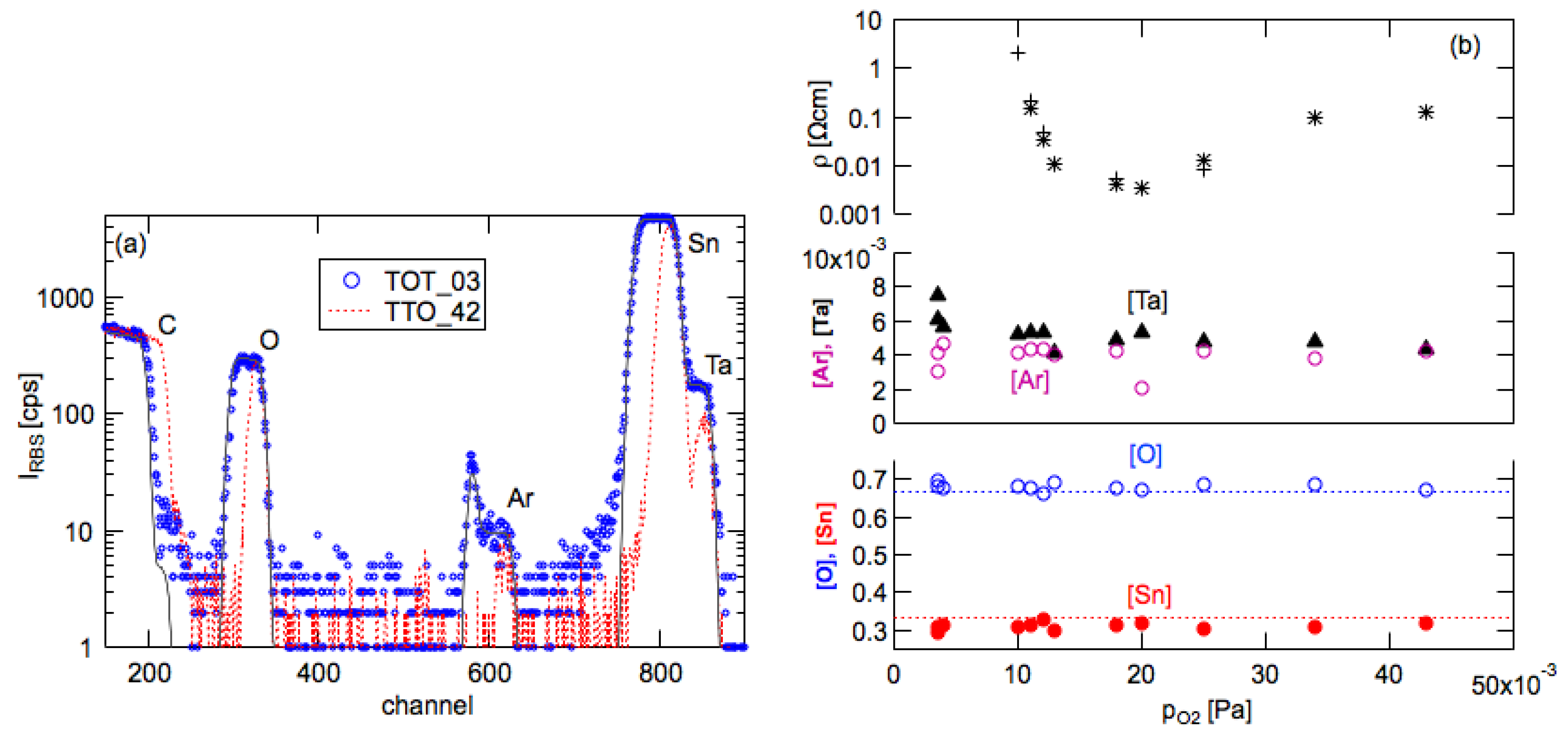
3.4. Film Composition (RBS)
- (i)
- Ar is implanted into the glassy carbon during the surface cleaning of the substrates by the Ar-RF plasma treatment (narrow peak at channel 590);
- (ii)
- Ar is included (buried) into the growing film during the deposition of the SnO2:Ta film. This is caused both by the continuous coverage of the film surface by neutral argon atoms from the sputtering atmosphere as well as the bombardment of the film surface by energetic Ar ions, atoms and metastable atoms [52,53] which are then covered by the film atoms.
3.5. Thickness Dependence
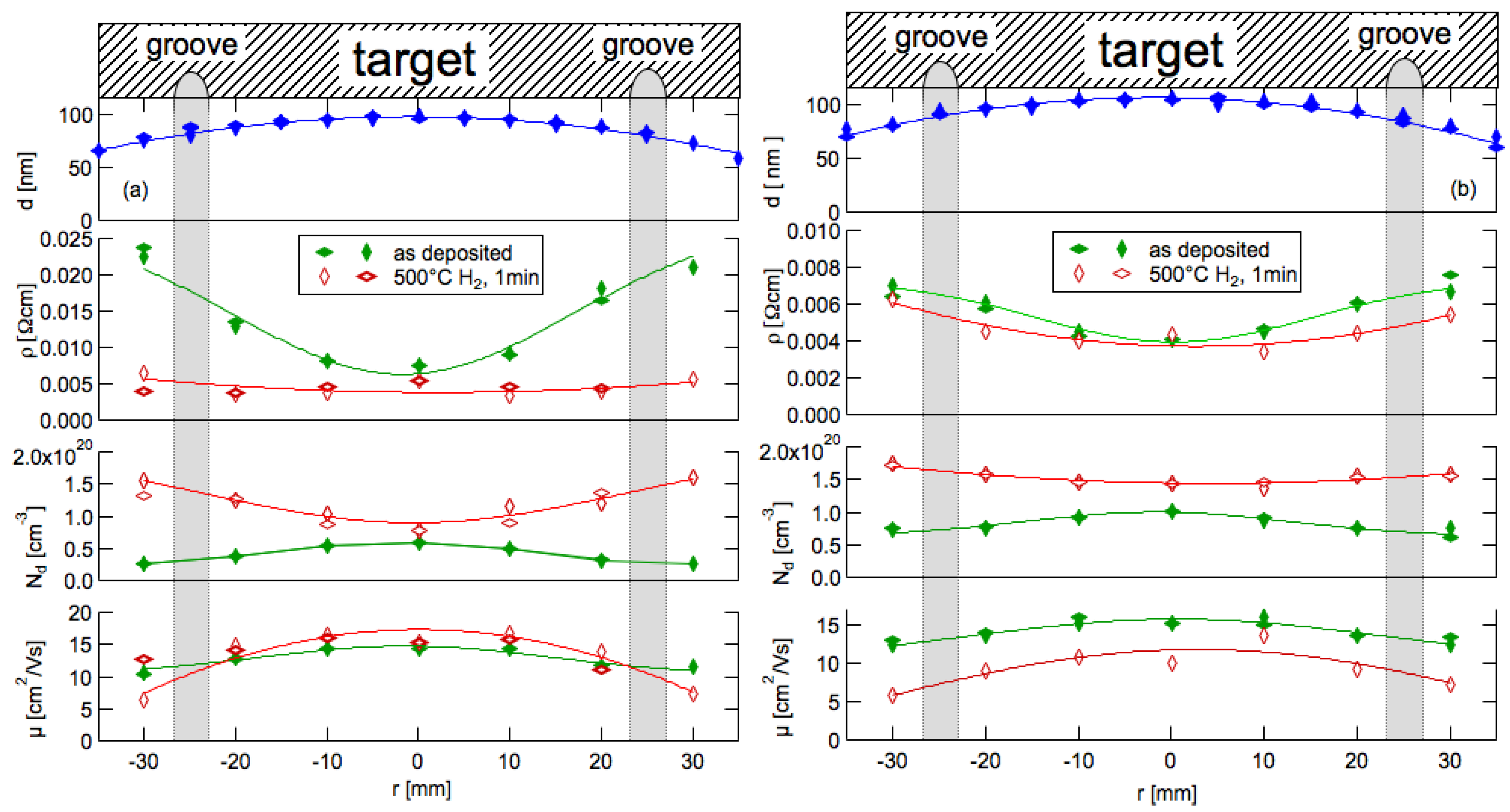
3.6. Radial Profiles
3.7. Transmittance and Reflectance
4. Conclusions
Author Contributions
Funding
Acknowledgments
Conflicts of Interest
References
- Hosono, H.; Kikuchi, N.; Ueda, N.; Kawazoe, H. Working hypothesis to explore novel wide band gap electrically conducting amorphous oxides and examples. J. Non Cryst. Solids 1996, 198, 165–169. [Google Scholar] [CrossRef]
- Hosono, H. Recent progress in transparent oxide semiconductors: Materials and device application. Thin Solid Films 2007, 515, 6000–6014. [Google Scholar] [CrossRef]
- Ellmer, K. Past achievements and future challenges in the development of optically transparent electrodes. Nat. Photonics 2012, 6, 809–817. [Google Scholar] [CrossRef]
- Vossen, J.L.; Kern, W. (Eds.) Thin Film Processes II; Academic Press: Cambridge, MA, USA, 1991; p. 866. [Google Scholar]
- Lungwitz, F.; Escobar-Galindo, R.; Janke, D.; Schumann, E.; Wenisch, R.; Gemming, S.; Krause, M. Transparent conductive tantalum doped tin oxide as selectively solartransmitting coating for high temperature solar thermal applications. Solar Ener. Mat. Solar Cells 2019, 196, 84–93. [Google Scholar] [CrossRef]
- Kavan, L.; Steier, L.; Grätzel, M. Ultrathin Buffer Layers of SnO2 by Atomic Layer Deposition: Perfect Blocking Function and Thermal Stability. J. Phys. Chem. C 2017, 121, 342–350. [Google Scholar] [CrossRef]
- Fischer, A. Dünne Halbleiterschichten auf Glas. Z. Naturforsch. 1954, 9, 508–511. [Google Scholar] [CrossRef][Green Version]
- Ishiguro, K.; Sasaki, T.; Arai, T.; Imai, I. Optical and Electrical Properties of Tin Oxide Films. J. Phys. Soc. Jap. 1958, 13, 296–304. [Google Scholar] [CrossRef]
- Shanthi, E.; Banerjee, A.; Dutta, V.; Chopra, K.L. Electrical and Optical Properties of Undoped and Antimony-Doped Tin Oxide Films. J. Appl. Phys. 1980, 51, 6243–6251. [Google Scholar] [CrossRef]
- Spence, W. The uv Absorption Edge of Tin Oxide Thin Films. J. Appl. Phys. 1967, 38, 3767–3770. [Google Scholar] [CrossRef]
- Weissmantel, C.; Fiedler, O.; Hecht, G.; Reisse, G. Ion beam sputtering and its application for the deposition of semiconducting films. Thin Solid Films 1972, 13, 359–366. [Google Scholar] [CrossRef]
- Manifacier, J.C. Thin Metallic Oxides as Transparent Conductors. Thin Solid Films 1982, 90, 297–308. [Google Scholar] [CrossRef]
- Stjerna, B.; Granqvist, C.G.; Seidel, A.; Häggström, L. Characterization of RF-Sputtered SnOx Thin Fims by Electron Microscopy, Hall-Effect Measurement, and Mössbauer Spectrometry. J. Appl. Phys. 1990, 68, 6241–6245. [Google Scholar] [CrossRef]
- Nakao, S.; Hirose, Y.; Fukumura, T.; Hasegawa, T. Carrier generation mechanism and effect of tantalum-doping in transparent conductive amorphous SnO2 thin films. Jap. J. Appl. Phys. 2014, 53, 5. [Google Scholar] [CrossRef]
- Goodchild, R.G.; Webb, J.B.; Williams, D.F. Electrical Properties of Highly Conducting and Transparent Thin Films of Magnetron Sputtered SnO2. J. Appl. Phys. 1985, 57, 2308–2310. [Google Scholar] [CrossRef]
- Handbook of Transparent Conductors; Ginley, D.S., Hosono, H., Paine, D.C., Eds.; Springer: New York, NY, USA, 2010; p. 534. [Google Scholar]
- Welzel, T.; Ellmer, K. Negative oxygen ion formation in reactive magnetron sputtering processes for transparent conductive oxides. J. Vac. Sci. Techn. A 2012, 30, 61306. [Google Scholar] [CrossRef]
- Ellmer, K.; Welzel, T. Reactive Magnetron Sputtering of Transparent Conductive Oxide Thin Films: Role of Energetic Particle (Ion) Bombardment. J. Mat. Res. 2012, 27, 765–779. [Google Scholar] [CrossRef]
- Schleife, A.; Varley, J.B.; Fuchs, F.; Rödl, C.; Bechstedt, F.; Rinke, P.; Janotti, A.; Walle, C.G.V.d. Tin dioxide from first principles: Quasiparticle electronic states and optical properties. Phys. Rev. B 2011, 83, 35116. [Google Scholar] [CrossRef]
- Ágoston, P.; Albe, K.; Nieminen, R.M.; Puska, M.J. Intrinsic n-Type Behavior in Transparent Conducting Oxides: A Comparative Hybrid-Functional Study of In2O3, SnO2, and ZnO. Phys. Rev. Lett. 2009, 103, 245501. [Google Scholar] [CrossRef]
- Minami, T. Transparent Conducting Oxide Semiconductors for Transparent Electrodes. Semicond. Sci. Techn. 2005, 20, S35–S44. [Google Scholar] [CrossRef]
- Ellmer, K. Resistivity of Polycrystalline Zinc Oxide Films: Current Status and Physical Limit. J. Phys. D Appl. Phys. 2001, 34, 3097–3108. [Google Scholar] [CrossRef]
- Ellmer, K.; Bikowski, A. Topical Review: Intrinsic and Extrinsic Doping of ZnO and ZnO Alloys. J. Phys. D 2016, 49, 413002. [Google Scholar] [CrossRef]
- Bellingham, J.R.; Phillips, W.A.; Adkins, C.J. Intrinsic Performance Limits in Transparent Conduction Oxides. J. Mat. Sci. Lett. 1992, 11, 263–265. [Google Scholar] [CrossRef]
- Chopra, K.L.; Major, S.; Pandya, D.K. Transparent Conductors- A Status Review. Thin Solid Films 1983, 102, 1–46. [Google Scholar] [CrossRef]
- Hartnagel, H.L.; Dawar, A.L.; Jain, A.K.; Jagadish, C. Semiconducting Transparent Thin Films; Institute of Physics Publishing: Bristol, UK, 1995; p. 358. [Google Scholar]
- Swallow, J.E.N.; Williamson, B.A.D.; Whittles, T.J.; Birkett, M.; Featherston, T.J.; Peng, N.; Abbott, A.; Farnworth, M.; Cheetham, K.J.; Warren, P.; et al. Self-Compensation in Transparent Conducting F-Doped SnO2. Adv. Funct. Mater. 2017, 28, 1701900. [Google Scholar] [CrossRef]
- Koch, H. Zum optischen Verhalten halbleitender Zinndioxydschichten im nahen Ultrarot bei Zimmertemperatur. phys. stat. sol. 1963, 3, 1619–1628. [Google Scholar] [CrossRef]
- Thornton, J.A. High Rate Sputtering Techniques. Thin Solid Films 1981, 80, 1–11. [Google Scholar] [CrossRef]
- Ellmer, K. Magnetron Discharges for Thin Film Deposition. In Low Temperature Plasmas. Fundamentals, Technologies and Techniques; Hippler, R., Kersten, H., Schmidt, M., Schoenbach, K.H., Eds.; Wiley-VCH: Berlin/Heidelberg, Germany, 2008; Volume 2, pp. 675–715. [Google Scholar]
- Kim, Y.-W.; Lee, S.W.; Chen, H. Microstructural evolution and electrical property of Ta-doped SnO2 films grown on Al2O3(0001) by metalorganic chemical vapor deposition. Thin Solid Films 2002, 405, 256–262. [Google Scholar] [CrossRef]
- Toyosaki, H.; Kawasaki, M.; Tokura, Y. Electrical properties of Ta-doped SnO2 thin films epitaxially grown on TiO2 substrate. Appl. Phys. Lett. 2008, 93, 132109. [Google Scholar] [CrossRef]
- Nakao, S.; Yamada, N.; Hitosugi, T.; Hirose, Y.; Shimada, T.; Hasegawa, T. High Mobility Exceeding 80 cm2 V−1s−1 in Polycrystalline Ta-Doped SnO2 Thin Films on Glass Using Anatase TiO2 Seed Layers. Appl. Phys. Express 2010, 3, 031102. [Google Scholar] [CrossRef]
- Weidner, M.; Jia, J.; Shigesato, Y.; Klein, A. Comparative study of sputter-deposited SnO2 films doped with antimony or tantalum. Phys. Stat. Sol 2016, 253, 923–928. [Google Scholar] [CrossRef]
- Muto, Y.; Oka, N.; Tsukamoto, N.; Iwabuchi, Y.; Kotsubo, H.; Shigesato, Y. High-rate deposition of Sb-doped SnO2 films by reactive sputtering using the impedance control method. Thin Soild Films 2011, 520, 1178–1181. [Google Scholar] [CrossRef]
- Jousse, D.; Constantino, C.; Chambouleyron, I. Highly Conductive and Transparent Amorphous Tin Oxide. J. Appl. Phys. 1983, 54, 431–434. [Google Scholar] [CrossRef]
- Nomura, K.; Ohta, H.; Takagi, A.; Kamiya, T.; Hirano, M.; Hosono, H. Room-Temperature Fabrication of Transparent Flexible Thin-Film Transistors Using Amorphous Oxide Semiconductors. Nature 2004, 432, 488–492. [Google Scholar] [CrossRef] [PubMed]
- Buchholz, D.B.; Ma, Q.; Alducin, D.; Ponce, A.; Jose-Yacaman, M.; Khanal, R.; Medvedeva, J.E.; Chang, R.P.H. The Structure and Properties of Amorphous Indium Oxide. Chem. Mater. 2014, 26, 5401–5411. [Google Scholar] [CrossRef]
- Hu, S.; Lewis, N.S.; Ager, J.W.; Yang, J.; McKone, J.R.; Strandwitz, N.C. Thin-Film Materials for the Protection of Semiconducting Photoelectrodes in Solar-Fuel Generators. J. Phys. Chem. C 2015, 115, 24201–24228. [Google Scholar] [CrossRef]
- Mayer, M. Ion Beam Analysis of Rough Thin Films. Nucl. Instr. Meth. Phys. Res. B Nucl. 2002, 194, 177–186. [Google Scholar] [CrossRef]
- Bikowski, A.; Welzel, T.; Ellmer, K. The correlation between the radial distribution of high-energetic ions and the structural as well as electrical properties of magnetron sputtered ZnO:Al films. J. Appl. Phys. 2013, 114, 223716. [Google Scholar] [CrossRef]
- Sigmund, P. Theory of Sputtering Yield of Amorphous and Polycrystalline Targets. Phys. Rev. 1969, 184, 383–416. [Google Scholar] [CrossRef]
- Yeom, G.Y.; Kushner, M.J. Cylindrical Magnetron Discharges. I. Current-Voltage Characteristics for DC- and RF-Driven Discharge Sources. J. Appl. Phys. 1989, 65, 3816–3824. [Google Scholar] [CrossRef]
- Ellmer, K. Magnetron Sputtering of Transparent Conductive Zinc Oxide: Relation between the Sputtering Parameters and the Electronic Properties. J. Phys. D Appl. Phys. 2000, 33, R17–R32. [Google Scholar] [CrossRef]
- Ruscic, B.; Feller, D.; Peterson, K.A. Active Thermochemical Tables: Dissociation energies of several homonuclear first-row diatomics and related thermochemical values. Theor. Chem. Acc. 2014, 133, 1415. [Google Scholar] [CrossRef]
- Kaufman, F. N20 Bond Dissociation Energy. J. Chem. Phys. 1967, 46, 2449. [Google Scholar] [CrossRef]
- Ellmer, K.; Cebulla, R.; Wendt, R. Characterization of a Magnetron Sputtering Discharge with Simultaneous RF-and DC-Excitation of the Plasma for the Deposition of Transparent and Conducting ZnO:Al-Films. Surf. Coat. Techn. 1998, 98, 1251–1256. [Google Scholar] [CrossRef]
- Nomura, K.; Kamiya, T.; Ohta, H.; Ueda, K.; Hirano, M.; Hosono, H. Carrier Transport in Transparent Oxide Semiconductor with Intrinsic Structural Randomness Probed Using Single-Crystalline InGaO3(ZnO)5 Films. Appl. Phys. Lett. 2004, 85, 1993–1995. [Google Scholar]
- Thienprasert, J.T.; Rujirawat, S.; Klysubun, W.; Duenow, J.N.; Coutts, T.J.; Zhang, S.B.; Look, D.C.; Limpijumnong, S. Compensation in Al-Doped ZnO by Al-Related Acceptor Complexes: Synchrotron X-Ray Absorption Spectroscopy and Theory. Phys. Rev. Lett. 2013, 110, 055502. [Google Scholar] [CrossRef]
- Bikowski, A.; Zajac, D.A.; Vinnichenko, M.; Ellmer, K. Evidence for the AlZn-Oi defect-complex model for magnetron-sputtered aluminium-doped zinc oxide: A combined X-ray absorption near edge spectroscopy, X-ray diffraction and electronic transport study. J. Appl. Phys. 2019, 126, 045106. [Google Scholar] [CrossRef]
- Tesmer, J.R.; Nastasi, M. (Eds.) Handbook of Modern Ion Beam Materials Analysis; MRS: Pittsburgh, PA, USA, 1995; p. 704. [Google Scholar]
- Winters, H.F.; Kay, E. Gas Incorporation into Sputtered Films. J. Appl. Phys. 1967, 38, 3928–3934. [Google Scholar] [CrossRef]
- Winters, H.F. Elementary Processes at Solid Surfaces Immersed in Low Pressure Plasmas. In Plasma Chemistry III; Veprek, S., Venugopalan, M., Eds.; Springer: Berlin/Heidelberg, Germany, 1980; Volume 94, pp. 69–125. [Google Scholar]
- Lee, W.W.Y.; Oblas, D. Argon entrapment in metal films by dc triode sputtering. J. Appl. Phys. 1975, 46, 1728–1732. [Google Scholar] [CrossRef]
- Thornton, J.A.; Hoffman, D.W. Internal Stresses in Amorphous Silicon Films Deposited by Cylindrical Magnetron Sputtering Using Ne, Ar, Kr, Xe, and Ar+H2. J. Vac. Sci. Techn. 1981, 18, 203–207. [Google Scholar] [CrossRef]
- Nie, M.; Bikowski, A.; Ellmer, K. Microstructure evolution of Al-doped zinc oxide and Sn-doped indium oxide deposited by radio-frequency magnetron sputtering: A comparison. J. Appl. Phys. 2015, 117, 155301. [Google Scholar] [CrossRef]
- Minami, T.; Nanto, H.; Takata, S. Highly Conducting and Transparent SnO2 Thin Films Prepared by RF Magnetron Sputtering on Low-Temperature Substrates. Jap. J. Appl. Phys. 1988, 27, L287–L289. [Google Scholar] [CrossRef]
- Brousseau, J.-L.; Bourque, H.; Tessier, A.; Leblanc, R.M. Electrical properties and topography of SnO2 thin films prepared by reactive sputtering. Appl. Surf. Sci. 1997, 108, 351–358. [Google Scholar] [CrossRef]
- Fuchs, K. The conductivity of thin metallic films according to the electron theory of metals. Proc. Cambridge Phil. Soc. 1938, 11, 100–108. [Google Scholar] [CrossRef]
- Sondheimer, E.H. The Mean Free Path of Electrons in Metals. Adv. Phys. 1952, 1, 1–42. [Google Scholar] [CrossRef]
- Ellmer, K.; Mientus, R.; Weiß, V.; Rossner, H. In situ Energy-Dispersive X-Ray Diffraction System for Time-Resolved Thin Film Growth Studies. Meas. Sci. Techn. 2003, 14, 336–345. [Google Scholar] [CrossRef]
- Kersten, H.; Deutsch, H.; Steffen, H.; Kroesen, G.M.W.; Hippler, R. The Energy Balance at Substrate Surfaces During Plasma Processing. Vacuum 2001, 63, 385–431. [Google Scholar] [CrossRef]
- Weise, M.; Seeger, S.; Harbauer, K.; Welzel, T.; Ellmer, K. A multifunctional plasma and deposition sensor for the characterization of plasma sources for film deposition and etching. J. Appl. Phys. 2017, 122, 044503. [Google Scholar] [CrossRef]
- Minami, T.; Oda, J.-I.; Nomoto, J.-I.; Miyata, T. Effect of Target Properties on Transparent Conducting Impurity-Doped ZnO Thin Films Deposited by DC Magnetron Sputtering. Thin Solid Films 2010, 519, 385–390. [Google Scholar] [CrossRef]
- Kluth, O.; Schöpe, G.; Rech, B.; Menner, R.; Oertel, M.; Orgassa, K.; Schock, H.W. Comparative Material Study on RF and DC Magnetron Sputtered ZnO:Al Films. Thin Solid Films 2006, 502, 311–316. [Google Scholar] [CrossRef]
- Szyszka, B. Magnetron Sputtering of ZnO Films. In Transparent Conductive Zinc Oxide: Basics and Application in Thin Film Solar Cells; Ellmer, K., Klein, A., Rech, B., Eds.; Springer: Berlin/Heidelberg, Germany, 2008; pp. 187–233. [Google Scholar]
- Hotop, H.; Lineberger, W.C. Binding Energies in Atomic Negative Ions. J. Phys. Chem. Ref. Data 1975, 4, 539–576. [Google Scholar] [CrossRef]
- Cuomo, J.J.; Gambino, R.J.; Harper, J.M.E.; Kuptsis, J.D. Origin and Effects of Negative Ions in the Sputtering of Intermetallic Compounds. IBM J. Res. Dev. 1977, 21, 580–583. [Google Scholar] [CrossRef]
- Burstein, E. Anomalous Optical Absorption Limit in InSb. Phys. Rev. 1954, 93, 632–633. [Google Scholar] [CrossRef]
- Moss, T.S. The Interpretation of the Properties of Indium Antimonide. Proc. Phys. Soc. Sec. B 1954, 67, 775–782. [Google Scholar] [CrossRef]


 15 WDC,
  25 WDC,
  100 WRF,
  30 WRF, ptotal = 0.5 Pa, RT.
15 WDC, 25 WDC, 100 WRF, 30 WRF, ptotal = 0.5 Pa, RT.
30 WRF, ptotal = 0.5 Pa, RT.
15 WDC, 25 WDC, 100 WRF, 30 WRF, ptotal = 0.5 Pa, RT.


© 2020 by the authors. Licensee MDPI, Basel, Switzerland. This article is an open access article distributed under the terms and conditions of the Creative Commons Attribution (CC BY) license (http://creativecommons.org/licenses/by/4.0/).
Share and Cite
Mientus, R.; Weise, M.; Seeger, S.; Heller, R.; Ellmer, K. Electrical and Optical Properties of Amorphous SnO2:Ta Films, Prepared by DC and RF Magnetron Sputtering: A Systematic Study of the Influence of the Type of the Reactive Gas. Coatings 2020, 10, 204. https://doi.org/10.3390/coatings10030204
Mientus R, Weise M, Seeger S, Heller R, Ellmer K. Electrical and Optical Properties of Amorphous SnO2:Ta Films, Prepared by DC and RF Magnetron Sputtering: A Systematic Study of the Influence of the Type of the Reactive Gas. Coatings. 2020; 10(3):204. https://doi.org/10.3390/coatings10030204
Chicago/Turabian StyleMientus, Rainald, Michael Weise, Stefan Seeger, Rene Heller, and Klaus Ellmer. 2020. "Electrical and Optical Properties of Amorphous SnO2:Ta Films, Prepared by DC and RF Magnetron Sputtering: A Systematic Study of the Influence of the Type of the Reactive Gas" Coatings 10, no. 3: 204. https://doi.org/10.3390/coatings10030204
APA StyleMientus, R., Weise, M., Seeger, S., Heller, R., & Ellmer, K. (2020). Electrical and Optical Properties of Amorphous SnO2:Ta Films, Prepared by DC and RF Magnetron Sputtering: A Systematic Study of the Influence of the Type of the Reactive Gas. Coatings, 10(3), 204. https://doi.org/10.3390/coatings10030204