Semiconducting p-Type Copper Iron Oxide Thin Films Deposited by Hybrid Reactive-HiPIMS + ECWR and Reactive-HiPIMS Magnetron Plasma System

 ,
, 
Abstract
:1. Introduction
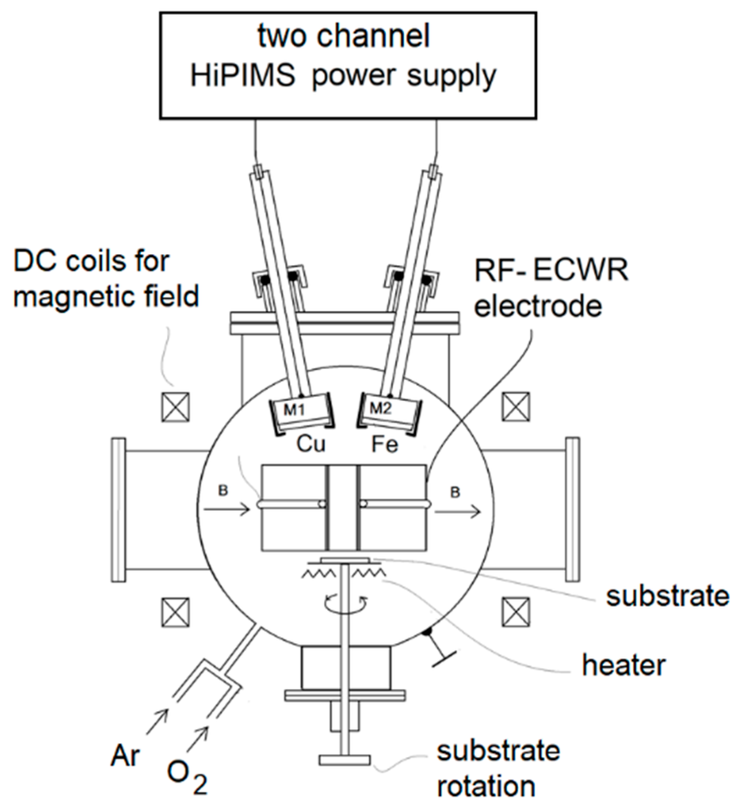
2. Experimental
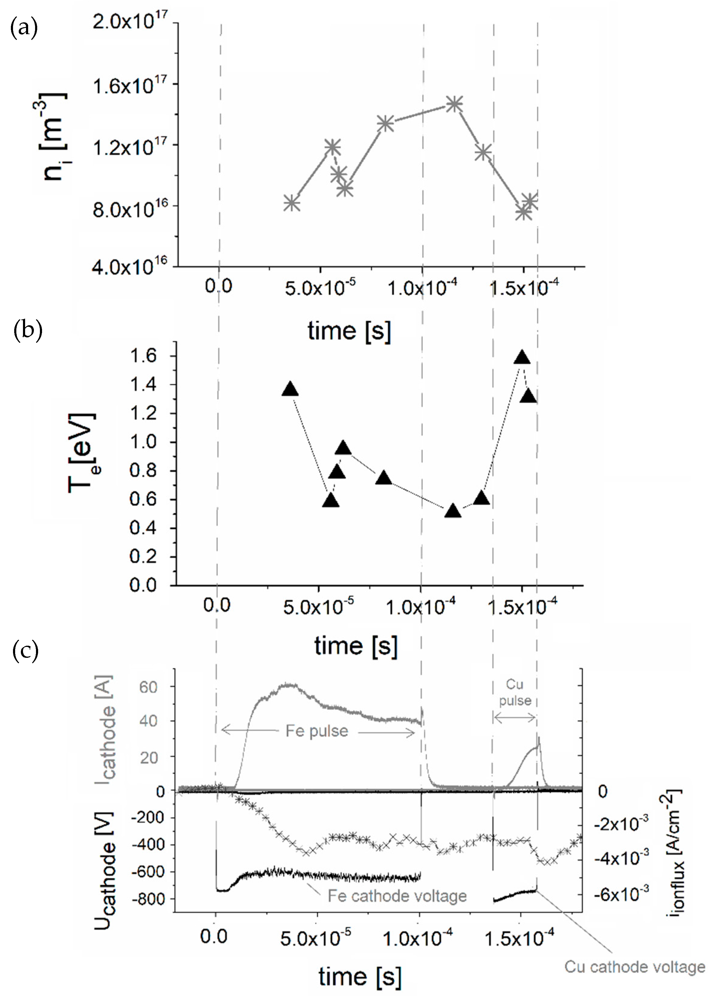
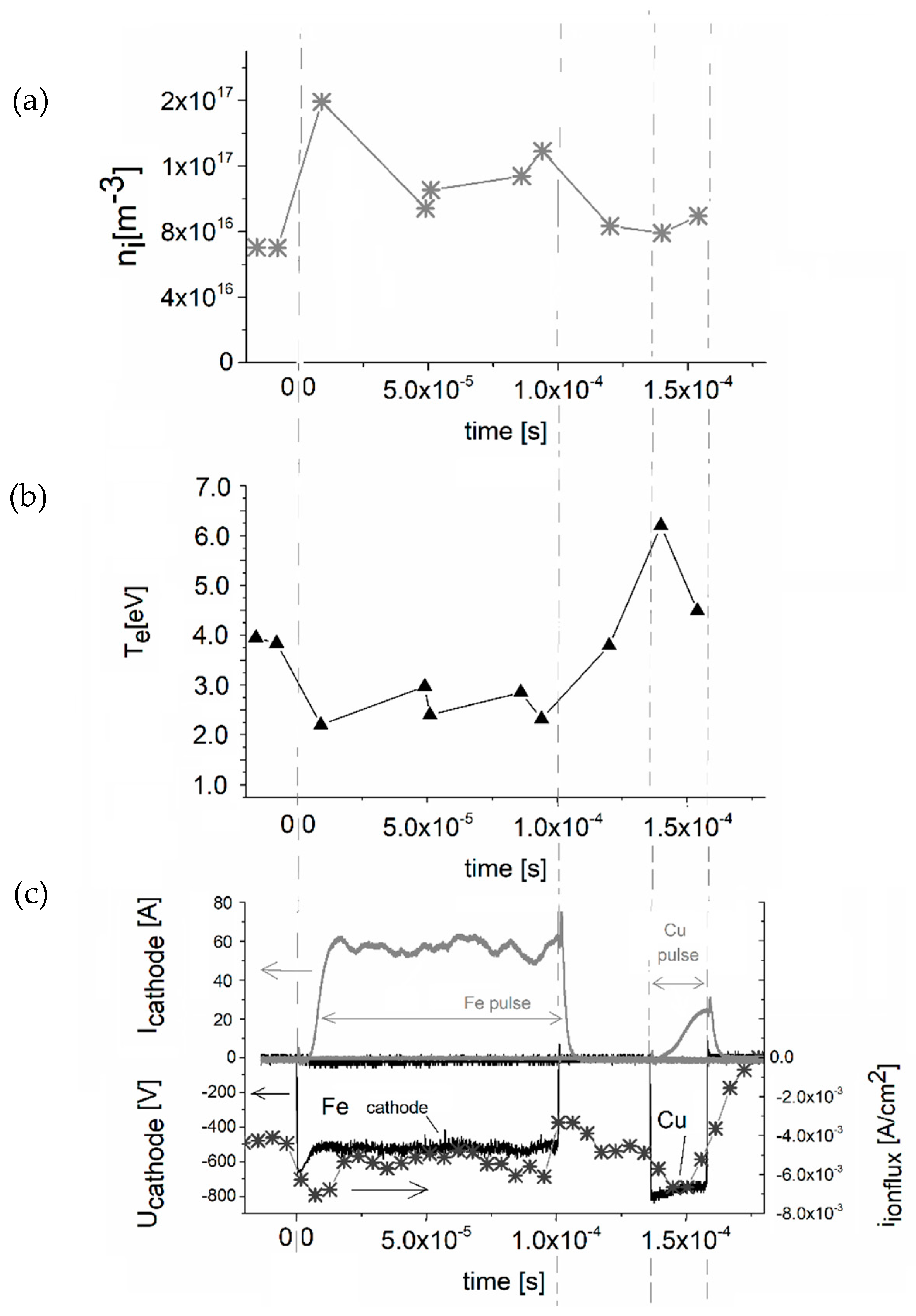
Plasma Diagnostics by RF Planar Probe
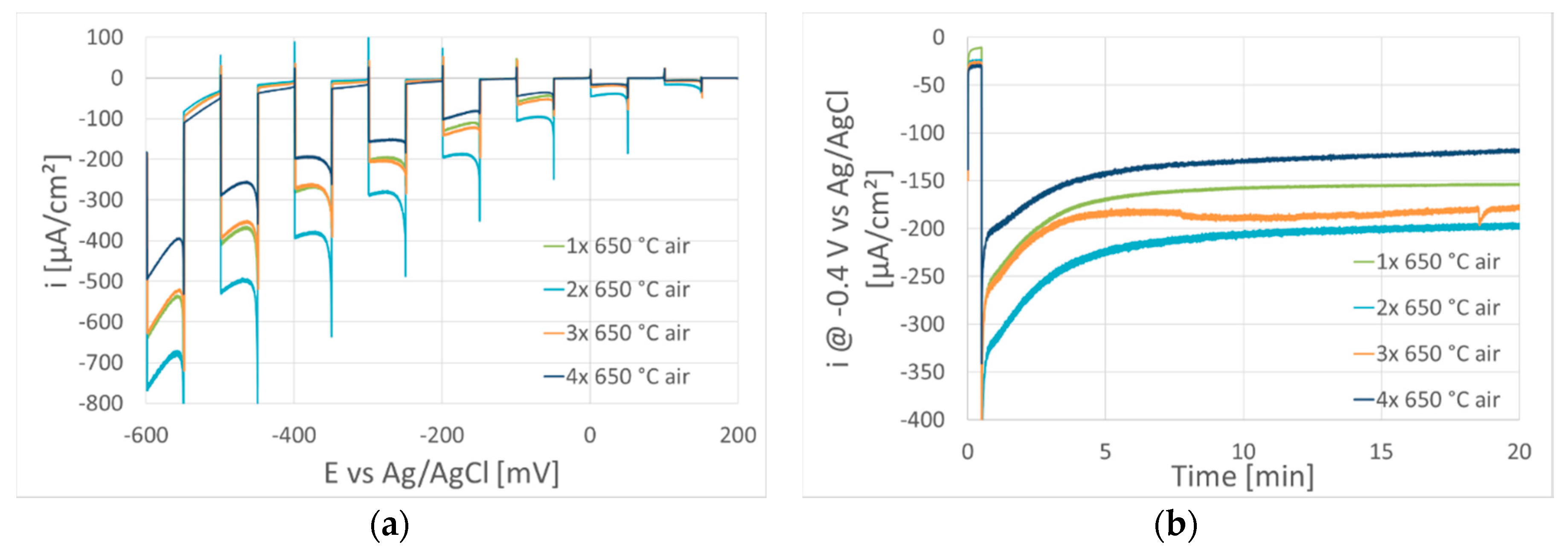
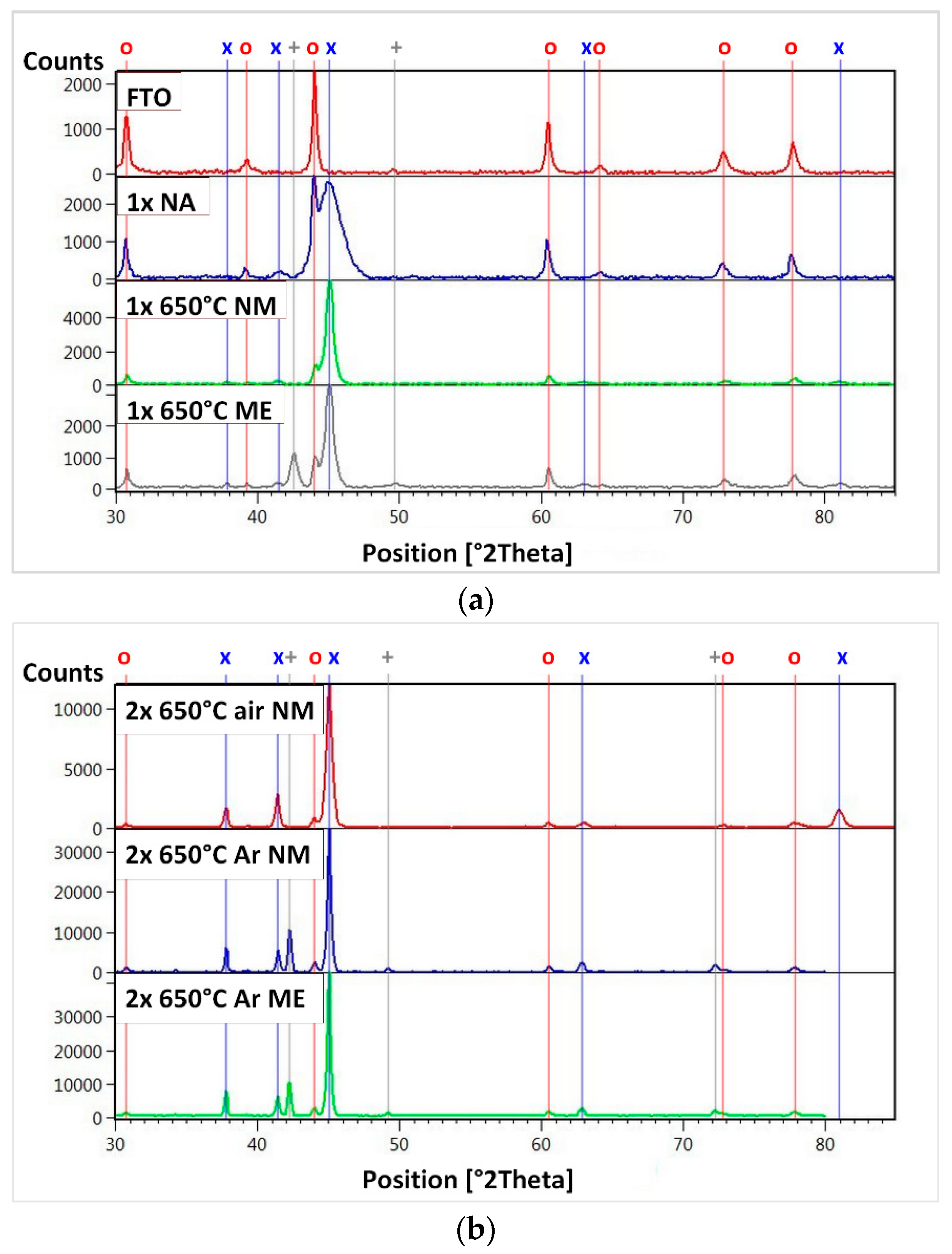
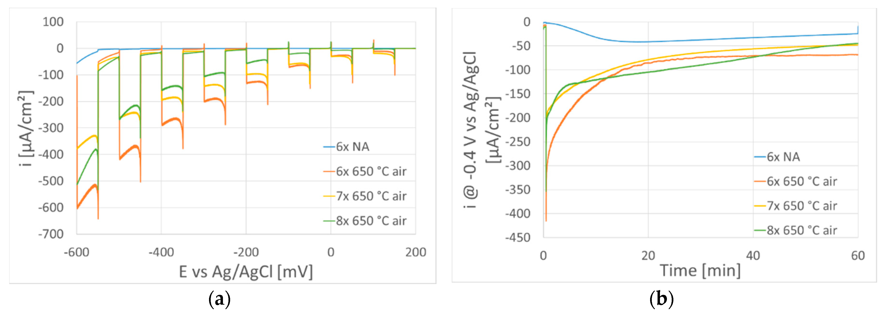
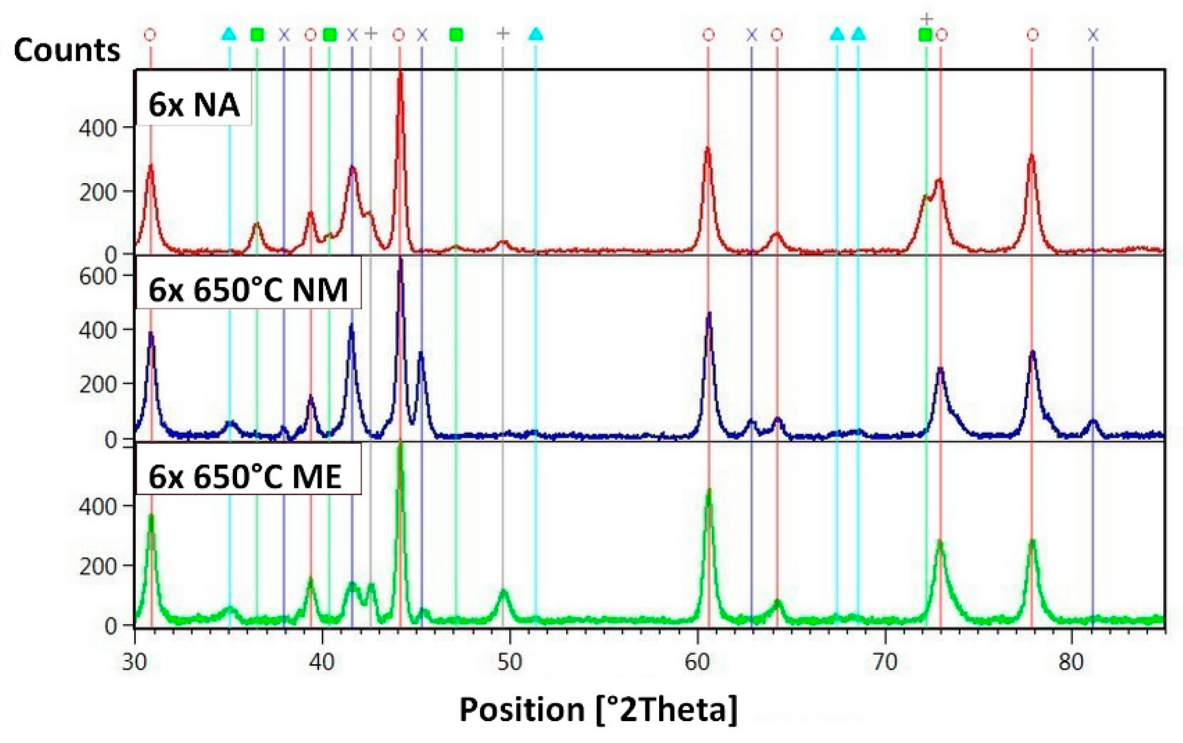
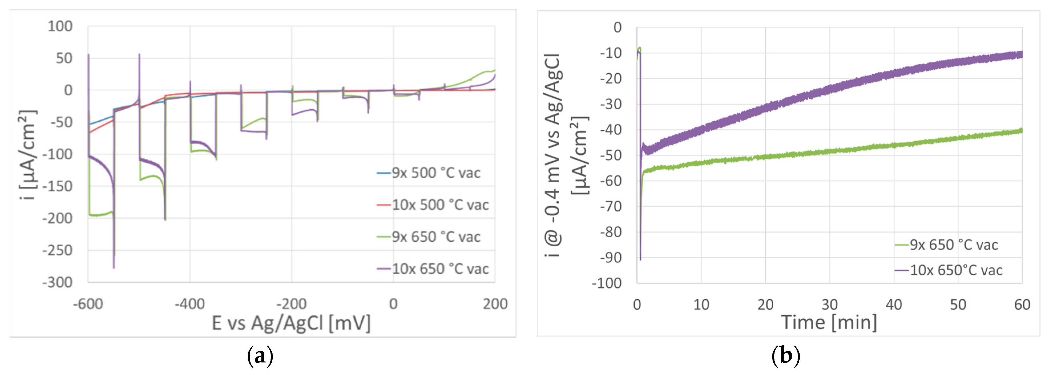
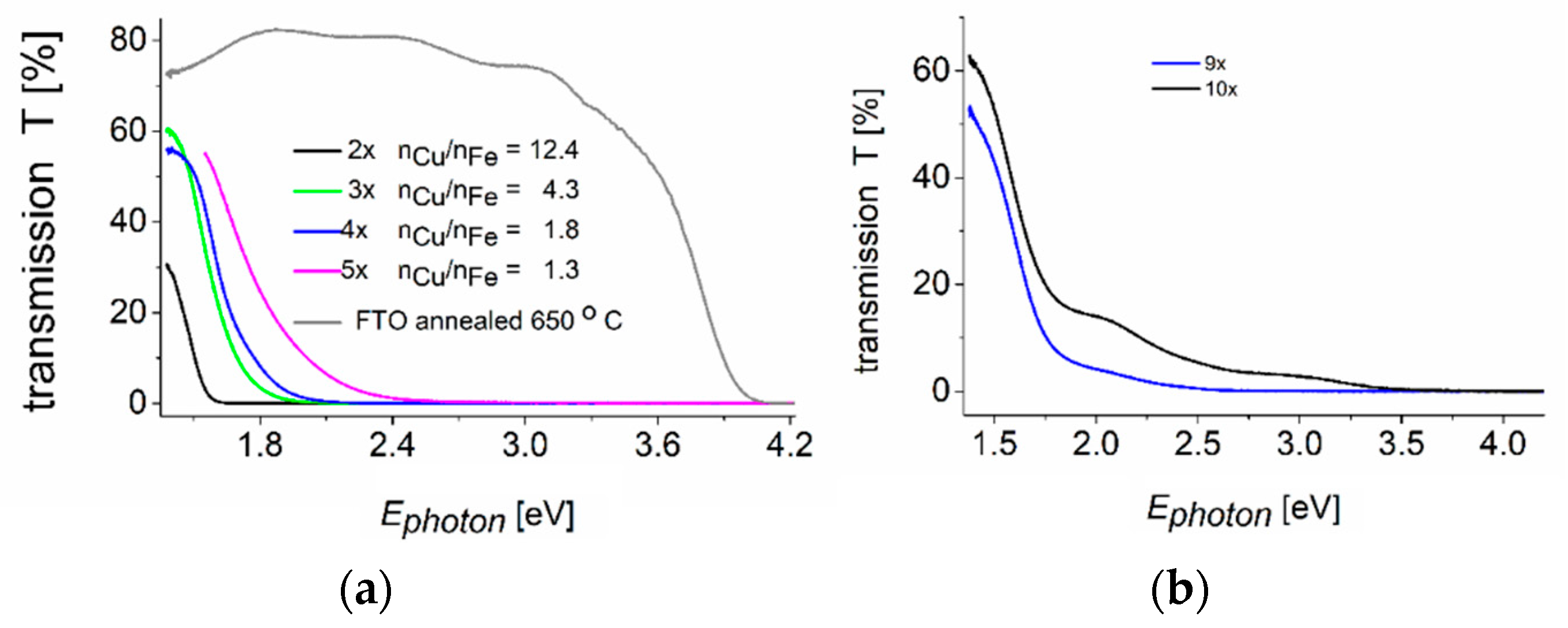
3. Results and Discussion
4. Conclusions
Supplementary Materials
Author Contributions
Funding
Conflicts of Interest
References
- Xiong, L.; Huang, S.; Yang, X.; Qiu, M.; Chen, Z.; Yu, Y. p-Type and n-type Cu2O semiconductor thin films: Controllable preparation by simple solvothermal method and photoelectrochemical properties. Electrochim. Acta 2011, 56, 2735–2739. [Google Scholar] [CrossRef]
- Paracchino, A.; Mathews, N.; Hisatomi, T.; Stefik, M.; Tilley, S.D.; Gratzel, M. Ultrathin films on copper(I) oxide water splitting photocathodes: A study on performance and stability. Energy Environ. Sci. 2012, 5, 8673–8681. [Google Scholar] [CrossRef]
- Panah, S.M.; Moakhar, R.S.; Chua, C.S.; Kushwaha, A.; Dalapati, G.K. Stable and efficient CuO based photocathode through oxygen-rich composition and Au–Pd nanostructure incorporation for solar-hydrogen production. ACS Appl. Mater. Interfaces 2017, 9, 27596–27606. [Google Scholar] [CrossRef] [PubMed]
- Crespo, C.T. Potentiality of CuFeO2-delafossite as a solar energy converter. Solar Energy 2018, 163, 162–166. [Google Scholar] [CrossRef]
- Prevot, M.S.; Guijarro, N.; Sivula, K. Enhancing the performance of a robust sol-gel-processed p-type delafossite CuFeO2 photocathode for solar water reduction. ChemSusChem 2015, 8, 1359–1367. [Google Scholar] [CrossRef] [PubMed]
- Husek, J.; Cirri, A.; Biswas, S.; Asthagiri, A.; Baker, L.R. Hole thermalization dynamics facilitate ultrafast spatial charge separation in CuFeO2 solar photocathodes. J. Phys. Chem. C 2018, 122, 11300–11304. [Google Scholar] [CrossRef]
- Du, F.; Chen, Q.; Wang, Y. Effect of annealing process on the heterostructure CuO/Cu2O as a highly efficient photocathode for photoelectrochemical water reduction. J. Phys. Chem. Solids 2017, 104, 139–144. [Google Scholar] [CrossRef]
- Rahman, M.; MacElroy, J.M.D.; Dowling, D.P. Influence of the physical, structural and chemical properties on the photoresponse property of magnetron sputtered TiO2 for the application of water splitting. J. Nanosci. Nanotechnol. 2011, 11, 8642–8651. [Google Scholar] [CrossRef]
- Krýsa, J.; Nemečková, A.; Zlámal, M.; Kotrla, T.; Baudys, M.; Kment, Š.; Hubička, Z.; Neumann-Spallart, M. α-Fe2O3/TiO2 stratified photoanodes. J. Photochem. Photobiol. A Chem. 2018, 366, 12–17. [Google Scholar] [CrossRef]
- Jia, L.; Harbauer, K.; Bogdanoff, P.; Ellmer, K.; Fiechter, S. Sputtering deposition of ultra-thin α-Fe2O3 films for solar water splitting. J. Mater. Sci. Technol. 2015, 31, 655–659. [Google Scholar] [CrossRef]
- Horiuchi, Y.; Mine, S.; Moriyasu, M.; Anpo, M.; Kim, T.H.; Matsuoka, M. Preparation of tantalum oxynitride thin film photocatalysts by reactive magnetron sputtering deposition under high substrate temperature. Res. Chem. Intermed. 2017, 43, 5123–5136. [Google Scholar] [CrossRef]
- Marsen, B.; Miller, E.L.; Paluselli, D.; Rocheleau, R.E. Progress in sputtered tungsten trioxide for photoelectrode applications. Int. J. Hydrog. Energy 2007, 32, 3110–3115. [Google Scholar] [CrossRef]
- Olejníček, J.; Brunclíková, M.; Kment, Š.; Hubička, Z.; Kmentová, H.; Kšírová, P.; Čada, M.; Zlámal, M.; Krýsa, J. WO3 thin films prepared by sedimentation and plasma sputtering. Chem. Eng. J. 2017, 318, 281–288. [Google Scholar] [CrossRef]
- Hubička, Z.; Zlámal, M.; Čada, M.; Kment, Š.; Krýsa, J. Photo-electrochemical stability of copper oxide photocathodes deposited by reactive high power impulse magnetron sputtering. Catal. Today 2019, 328, 29–34. [Google Scholar] [CrossRef]
- Patel, M.; Kim, H.S.; Patel, D.B.; Kim, J. CuO photocathode-embedded semitransparent photoelectrochemical cell. J. Mater. Res. 2016, 31, 3205–3213. [Google Scholar] [CrossRef]
- Xie, T.; Zheng, T.; Wang, R.; Bu, Y.; Ao, J.P. Fabrication of CuOx thin-film photocathodes by magnetron reactive sputtering for photoelectrochemical water reduction. Green Energy Environ. 2018, 3, 239–246. [Google Scholar] [CrossRef]
- Jiang, C.M.; Reyes-Lillo, S.E.; Liang, Y.; Liu, Y.S.; Liu, G.; Toma, F.M.; Prendergast, D.; Sharp, I.D.; Cooper, J.K. Electronic structure and performance bottlenecks of CuFeO2 photocathodes. Chem. Mater. 2019, 31, 2524–2534. [Google Scholar] [CrossRef]
- Vasina, P.; Fekete, M.; Hnilica, J.; Klein, P.; Dosoudilova, L.; Dvorak, P.; Navratil, Z. Determination of titanium atom and ion densities in sputter deposition plasmas by optical emission spectroscopy. Plasma Sources Sci. Technol. 2015, 24, 065022. [Google Scholar] [CrossRef]
- Ehiasarian, A.P.; Gonzalvo, Y.A.; Whitmore, T.D. Time-resolved ionisation studies of the high power impulse magnetron discharge in mixed argon and nitrogen atmosphere. Plasma Process. Polym. 2007, 4, S309–S313. [Google Scholar] [CrossRef]
- Peng, W.C.; Chen, Y.C.; He, J.L.; Ou, S.L.; Horng, R.H.; Wuu, D.S. Tunability of p- and n-channel TiOx thin film transistors. Sci. Rep.-UK 2018, 8, 9255. [Google Scholar] [CrossRef] [Green Version]
- Tiron, V.; Velicu, I.L.; Stanescu, D.; Magnan, H.; Sirghi, L. High visible light photocatalytic activity of nitrogen-doped ZnO thin films deposited by HiPIMS. Surf. Coat Technol. 2017, 324, 594–600. [Google Scholar] [CrossRef] [Green Version]
- Cemin, F.; Tsukamoto, M.; Keraudy, J.; Antunes, V.G.; Helmersson, U.; Alvarez, F.; Minea, T.; Lundin, D. Low-energy ion irradiation in HiPIMS to enable anatase TiO2 selective growth. J. Phys. D Appl. Phys. 2018, 51, 235301. [Google Scholar] [CrossRef]
- Kouznetsov, V.; Macák, K.; Schneider, J.M.; Helmersson, U.; Petrov, I. A novel pulsed magnetron sputter technique utilizing very high target power densities. Surf. Coat. Technol. 1999, 122, 290–293. [Google Scholar] [CrossRef]
- Helmersson, U.; Lattemann, M.; Bohlmark, J.; Ehiasarian, A.P.; Gudmundsson, J.T. Ionized physical vapor deposition (IPVD): A review of technology and applications. Thin Solid Films 2006, 513, 1–24. [Google Scholar] [CrossRef] [Green Version]
- Cemin, F.; Abadias, G.; Minea, T.; Furgeaud, C.; Brisset, F.; Solas, D.; Lundin, D. Benefits of energetic ion bombardment for tailoring stress and microstructural evolution during growth of Cu thin films. Acta Mater. 2017, 141, 120–130. [Google Scholar] [CrossRef]
- Anders, A. Tutorial: Reactive high power impulse magnetron sputtering (R-HiPIMS). J. Appl. Phys. 2017, 121, 171101. [Google Scholar] [CrossRef] [Green Version]
- Anders, A.; Čapek, J.; Hála, M.; Martinu, L. The ‘recycling trap’: A generalized explanation of discharge runaway in high-power impulse magnetron sputtering. J. Phys. D Appl. Phys. 2012, 45, 012003. [Google Scholar] [CrossRef]
- Poolcharuansin, P.; Bowes, M.; Petty, T.J.; Bradley, J.W. Ionized metal flux fraction measurements in HiPIMS discharges. J. Phys. D Appl. Phys. 2012, 45, 322001. [Google Scholar] [CrossRef]
- Straňák, V.; Herrendorf, A.P.; Drache, S.; Čada, M.; Hubička, Z.; Tichý, M.; Hippler, R. Highly ionized physical vapor deposition plasma source working at very low pressure. Appl. Phys. Lett. 2012, 100, 141604. [Google Scholar] [CrossRef]
- Straňák, V.; Herrendorf, A.P.; Drache, S.; Čada, M.; Hubička, Z.; Bogdanowicz, R.; Tichy, M.; Hippler, R. Plasma diagnostics of low pressure high power impulse magnetron sputtering assisted by electron cyclotron wave resonance plasma. J. Appl. Phys. 2012, 112, 093305. [Google Scholar] [CrossRef] [Green Version]
- Straňák, V.; Hubička, Z.; Čada, M.; Drache, S.; Tichý, M.; Hippler, R. Investigation of ionized metal flux in enhanced high power impulse magnetron sputtering discharges. J. Appl. Phys. 2014, 115, 153301. [Google Scholar] [CrossRef]
- Straňák, V.; Herrendorf, A.P.; Wulff, H.; Drache, S.; Čada, M.; Hubička, Z.; Tichý, M.; Hippler, R. Deposition of rutile (TiO2) with preferred orientation by assisted high power impulse magnetron sputtering. Surf. Coat. Technol. 2013, 222, 112–117. [Google Scholar] [CrossRef]
- Straňák, V.; Hubička, Z.; Čada, M.; Bogdanowicz, R.; Wulff, H.; Helm, C.A.; Hippler, R. Influence of reactive oxygen species during deposition of iron oxide films by high power impulse magnetron sputtering. J. Phys. D Appl. Phys. 2018, 51, 095205. [Google Scholar] [CrossRef]
- Sezemský, P.; Straňák, V.; Kratochvíl, J.; Čada, M.; Hippler, R.; Hrabovský, M.; Hubicka, Z. Modified high frequency probe approach for diagnostics of highly reactive plasma. Plasma Sources Sci. Technol. 2019, 28, 115009. [Google Scholar] [CrossRef]
- Sobolewski, M.A. Measuring the ion current in electrical discharges using radio-frequency current and voltage measurements. Appl. Phys. Lett. 1998, 72, 1146–1148. [Google Scholar] [CrossRef]
- Sobolewski, M.A. Measuring the ion current in high-density plasmas using radio-frequency current and voltage measurements. J. Appl. Phys. 2001, 90, 2660. [Google Scholar] [CrossRef]
- Sobolewski, M.A.; Lahr, D.L. Origin of electrical signals for plasma etching end point detection: Comparison of end point signals and electron density. Vac. Sci. Technol. A 2012, 30, 051303. [Google Scholar] [CrossRef]
- Murali, D.S.; Kumar, S.; Choudhary, R.J.; Wadikar, A.D.; Jain, M.K.; Subrahmanyam, A. Synthesis of Cu2O from CuO thin films: Optical and electrical properties. AIP Adv. 2015, 5, 047143. [Google Scholar] [CrossRef]


| Sample | IFeav [mA] | UFe [V] | ICuav [mA] | UCu [V] | QO₂ [sccm] | tdep. [°C] | Thickness [nm] | mol. Ratio Cu/Fe | PECWR [W] |
|---|---|---|---|---|---|---|---|---|---|
| 1x | 500 | 720 | 84 | 975 | 10 | 250 | 900 | 4.77 | 180 |
| 2x | 500 | 720 | 176 | 1000 | 10 | 250 | 2200 | 12.35 | 180 |
| 3x | 600 | 720 | 56 | 1000 | 10 | 250 | 580 | 4.27 | 180 |
| 4x | 500 | 720 | 50 | 895 | 5 | 250 | 535 | 1.79 | 180 |
| 5x | 550 | 600 | 40 | 841 | 5 | 250 | 250 | 1.33 | 180 |
| 6x | 440 | 700 | 42 | 834 | 2 | 500 | 350 | 0.82 | 0 |
| 7x | 400 | 700 | 47 | 816 | 1.3 | 500 | 600 | 0.82 | 0 |
| 8x | 500 | 700 | 44 | 842 | 3.2 | 500 | 300 | 0.79 | 0 |
| 9x | 500 | 700 | 40 | 804 | 2 | 500 | 400 | 0.94 | 0 |
| 10x | 500 | 700 | 30 | 789 | 2 | 500 | 240 | 0.86 | 0 |
| Phase | Semiquantitative Phase Composition/% | |||
|---|---|---|---|---|
| 9x 650 °C vac NM | 9x 650 °C vac ME | 10x 650 °C vac NM | 10x 650 °C vac ME | |
| CuFeO2 | 67 | 29 | 80 | 100 |
| Cu2O | 33 | 43 | 20 | – |
| Fe3O4 | – | 28 | – | – |
© 2020 by the authors. Licensee MDPI, Basel, Switzerland. This article is an open access article distributed under the terms and conditions of the Creative Commons Attribution (CC BY) license (http://creativecommons.org/licenses/by/4.0/).
Share and Cite
Hubička, Z.; Zlámal, M.; Olejníček, J.; Tvarog, D.; Čada, M.; Krýsa, J. Semiconducting p-Type Copper Iron Oxide Thin Films Deposited by Hybrid Reactive-HiPIMS + ECWR and Reactive-HiPIMS Magnetron Plasma System. Coatings 2020, 10, 232. https://doi.org/10.3390/coatings10030232
Hubička Z, Zlámal M, Olejníček J, Tvarog D, Čada M, Krýsa J. Semiconducting p-Type Copper Iron Oxide Thin Films Deposited by Hybrid Reactive-HiPIMS + ECWR and Reactive-HiPIMS Magnetron Plasma System. Coatings. 2020; 10(3):232. https://doi.org/10.3390/coatings10030232
Chicago/Turabian StyleHubička, Zdenek, Martin Zlámal, Jiri Olejníček, Drahoslav Tvarog, Martin Čada, and Josef Krýsa. 2020. "Semiconducting p-Type Copper Iron Oxide Thin Films Deposited by Hybrid Reactive-HiPIMS + ECWR and Reactive-HiPIMS Magnetron Plasma System" Coatings 10, no. 3: 232. https://doi.org/10.3390/coatings10030232
APA StyleHubička, Z., Zlámal, M., Olejníček, J., Tvarog, D., Čada, M., & Krýsa, J. (2020). Semiconducting p-Type Copper Iron Oxide Thin Films Deposited by Hybrid Reactive-HiPIMS + ECWR and Reactive-HiPIMS Magnetron Plasma System. Coatings, 10(3), 232. https://doi.org/10.3390/coatings10030232