1. Introduction
The efficient utilization of solar energy occupies the essential position for addressing energy and environmental conflicts. To achieve the optimized conversion of solar energy, an appropriate semiconductor, such as TiO
2, NiO, ZnO, CdS, or Fe
2O
3, among others [
1], should be used as a photocatalyst. TiO
2 has attracted increasing attention due to its chemical stability, environmental friendliness, and simple preparation [
2]. Rutile TiO
2 photoelectrode can split H
2O into H
2 and O
2 with a volume ratio of 2:1 under the action of near-ultraviolet light (~380 nm) [
3]. However, the wide band gap of TiO
2 is 3.2 eV for anatase and 3.0 eV for rutile, respectively. The response spectrum is mainly in the ultraviolet region and the photogenerated electron-hole pair has high recombination probability, which limits the practical application of TiO
2 [
4].
So far, it is found that TiO
2 doped with metal or non-metal elements can improve its absorption of visible light resulting in the increasing yield of photogenerated electron-hole pairs [
5,
6,
7]. Non-metal doped TiO
2 is mainly acquired by non-metal atoms substituting the oxygen atoms in the crystal lattice or fitting into the interstitial sites [
8,
9]. Metal-doped TiO
2 with metal ions introduced into the TiO
2 crystal lattice has the advantages of the formation of defects which inhibit the recombination of photo-generated carriers, and also bring impurity levels for regulating the energy band structure [
5]. Recently, the doping of transition metal elements such as Mo [
10], Fe [
11], Mn [
12], Cr [
13], V [
14], and Ni [
15] have been investigated for the purpose of enhancing the photocatalytic efficiency of TiO
2. Wu et al. [
11] prepared Fe-TiO
2 nanotubes with the ultrasonic impregnation-calcination method. It was found that some of the Fe
3+ ions entered into the TiO
2 lattice, and the absorption capacity of visible light of Fe-doped TiO
2 nanotube arrays gradually increases as the doping amount increases. Patle et al. [
16] reported an one-step co-precipitation method of synthesizing TiO
2 nanoparticles with Mn
2+, Cu
2+, and Fe
2+, and assembling dye-sensitized solar cells (DSSCs) using doped-TiO
2 nanoparticles as photoanode. Compared with TiO
2 photoanode materials without Cu
2+ and Fe
2+ doping, the incorporation of Mn
2+ can effectively increase the light conversion efficiency of TiO
2. Avansi et al. [
17] synthesized V-doped TiO
2 nanostructures and observed single-crystalline anatase phase despite the different amounts of V ions. Li et al. [
15] reported a novel Ni-doped TiO
2 inverse opal photonic microarray (IOPM) structure photocatalyst and Ni doping could increase the visible light absorption. Recent studies indicate that the radius of Mo
6+ is similar to that of Ti
4+, thus, compared with other transition metal elements, Mo can effectively replace Ti
4+ in TiO
2 crystal lattice [
18,
19]. The doping donates a contribution to redshift as the absorption edge moving towards the region of visible light and improve the light response under both ultraviolet and visible light as well, enhancing the photoelectrochemical activity of TiO
2 [
7,
18]. Wang et al. [
20] prepared Mo-doped TiO
2 nanoparticles through the sol-gel method, where the band gap of TiO
2 can be reduced from 3.19 to 3.05 eV with an increase in doping concentration, and the photocatalytic ability of TiO
2 nanoparticles reached the best level at 2.0 at.% Mo doping. Huang et al. [
7] studied the effects of annealing temperature and Mo doping concentration on crystalline phase, grain size, lattice distortion, and photoresponse, which indicates most doped Mo
6+ ions replace Ti
4+ in the TiO
2, and the grain growth and phase transformation of TiO
2 are suppressed, resulting in the distortion of the TiO
2 crystal lattice. Liao et al. [
21] found that doping with Mo in a sol-gel method can improve the electrochemical performance of TiO
2. This is mainly due to the induction of electrons in the conduction band, as well as oxygen defects including vacancies in the band gap increasing the conductivity. Studies listed above show that Mo-doped TiO
2 has the potential development of promising photocatalytic properties under UV/visible light, and it is very meaningful to optimize the doping amount in a simple and controllable way.
However, recent works on controllable Mo doping TiO
2 by the sol-gel method often resulted in nanoparticles rather than nanotubes [
7], and other works on TiO
2 nanotubes doping are often achieved with a surface modified or deposited with metal particles [
22], which cannot guarantee the overall doping of the nanotubes as well as the precise control of the doping content. Hence, the growing of TiO
2 nanotubes array with flexible Mo doping still requires exploration.
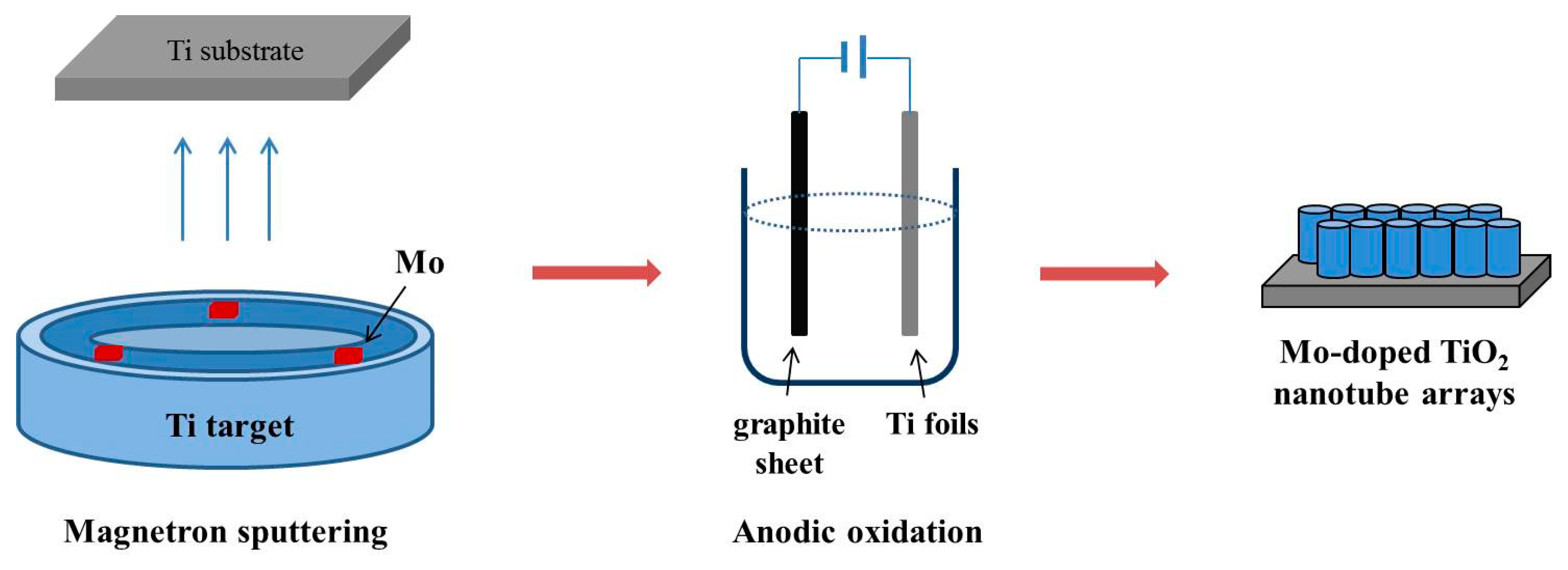
Pure TiO2 nanotubes are generally fabricated by anodization in F−-based electrolyte (pH < 5), uniformly grown atop the supporting titanium metal foil substrates, during which, however, the overall doping of nanotubes can hardly be achieved, and the component controllability is difficult to reach even under various chemical methods. Therefore, the initial doping modification of pure Ti substrates is of great necessity in order to fabricate a Mo-doped nanotube array through the Ti–Mo alloy film.
In our experiment, Mo-doped TiO2 was prepared by combining a magnetron sputtering and anodic oxidation method. We creatively proposed a magnetron sputtering technique to fulfill adjustable dose of Ti–Mo thin films through regulating the atomic ratio of target materials. Then, Mo-doped TiO2 nanotube arrays were prepared by oxidizing Ti–Mo alloy films. The enhanced photoelectrochemical performance was demonstrated for the Mo-TiO2 nanotubes as photoelectrode. This combination of magnetron sputtering and electrochemical oxidation method of preparing doped TiO2 with nanotubular morphology aligned perpendicular to the surface of substrates provides some advantages for carrier transport performance among nanotubes as well as between the interfaces of semiconductor and the metal substrate resulting in accelerated separation of photogenerated carriers.
2. Experimental Section
Ti–Mo alloy films were physically deposited on titanium foils at room temperature in a DC magnetron vacuum deposition machine (SY-500, Beijing Shengdeyu Vacuum Technology Co., Beijing, China). Before sputtering, titanium foils (0.1 mm thickness, 99.6% purity) were ultrasonically cleaned with acetone, ethanol, and deionized water sequentially, then chemically etched by dipping in a mixture solution of HF (40%), HNO3 (65%), and deionized water (1:4:5 in volume) for 1 min (30 seconds on each side), rinsed with deionized water and dried by N2. Four Ti targets (99.99%, Alluter, Shenzhen, China) embedded with different amounts of Mo (0%, 0.25%, 0.5%, 1.0%) were also prepared beforehand, regulated by attaching several Mo cubes (2 mm × 2 mm × 2 mm) to different symmetric areas on the sputtering ring of Ti target so as to control the Mo content in each target. It should be noted that the content of Mo is supposed to be accurately confirmed or calibrated due to the deviation of sputtering yields to some extent. Before sputtering, the vacuum pressure inside the cavity reached 2.5 × 10⁻³ Pa and each sputtering process lasted 40 min, in a pressure of 0.5 Pa (Ar (100%)) with a power of 200 W. The as-prepared Ti–Mo film owed a thickness of 300 nm at least.
The preparation of Mo-doped TiO
2 nanotube arrays by anodization method could be widely found [
23]. Briefly, we performed it with the Ti foils (deposited with Ti–Mo alloy films on the top) as the working electrode and a graphite sheet as the counter electrode bathing in a 0.5 wt.% HF solution anodized for 40 min under a voltage of 20 V with DC power. The as-prepared samples were quickly rinsed in pure water afterwards, dried with an air stream, and annealed at 500 °C for 2 h under ambient conditions. The fabricated TiO
2 nanotube array is observed with an approximate length of 300 nm, which indicates that Ti–Mo film deposited on the Ti substrate is not completely etched. The content of Mo doped TiO
2 is controlled by the number of Mo cubes used in magnetron sputtering, marked as Mo1.0 (1.0 at.% Mo), Mo0.5 (0.5 at.% Mo), Mo0.25 (0.25 at.% Mo), and Mo0 (0 at.% Mo), respectively.
Figure 1 gives a brief illustration of the preparation of Mo-doped TiO
2 nanotube arrays in this study.
The details of measurement can be found elsewhere [
24].
3. Results and Discussion
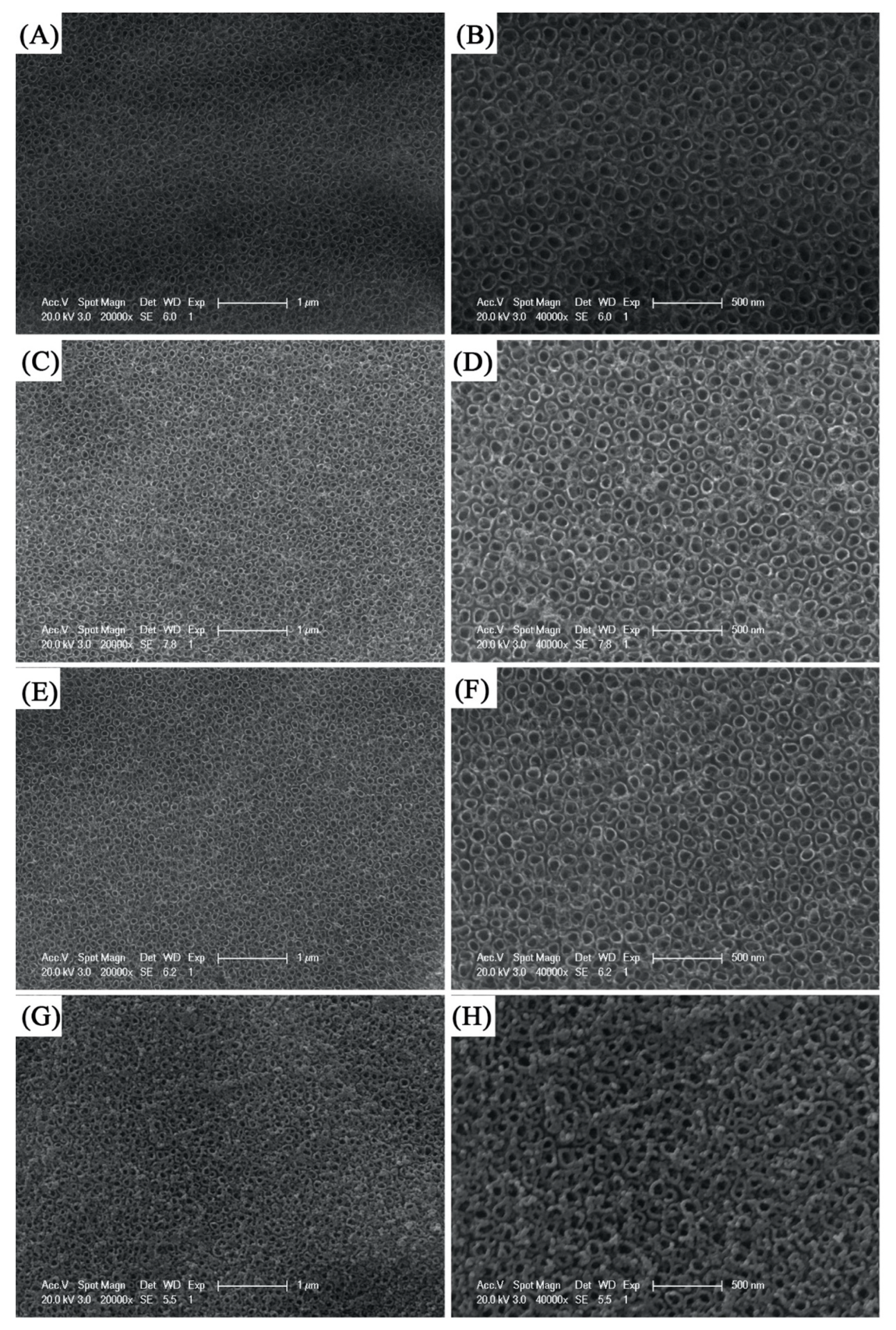
The morphology of the pure TiO
2 and Mo-doped TiO
2 nanotube arrays was characterized by scanning electron microscope (SEM, XL30FEG, Philips, Eindhoven, The Netherlands) as shown in
Figure 2. This illustrates that the TiO
2 nanotube arrays with an observed hollow structure were successfully fabricated by the controllable one-step anodization procedure. A top view of TiO
2 nanotubes with different Mo doping concentrations is shown as
Figure 2A–H. Uniformly ordered and vertically grown Mo doped TiO
2 nanotubes with an approximately inner diameter of 80 nm and a wall thickness of around 10 nm were formed from Ti–Mo film on Ti substrates, while the undoped TiO
2 nanotube array grew with an inner diameter range of 50–100 nm and a thickness of 25 nm. It can be predicted that when the content of Mo doping gradually decreases, the degree of damage to the hollow structure of the nanotube will be correspondingly reduced. In addition, the center spacing of adjacent nanotubes increases with the decrease of Mo doping content, which indicates that the arrangement density of nanotube array increases with the decrease of Mo doping content. By comparison, it is possible that Mo doping content governs the destruction of the TiO
2 nanotube structure and the introduction of impurities and defects in the film prepared by magnetron sputtering [
8].
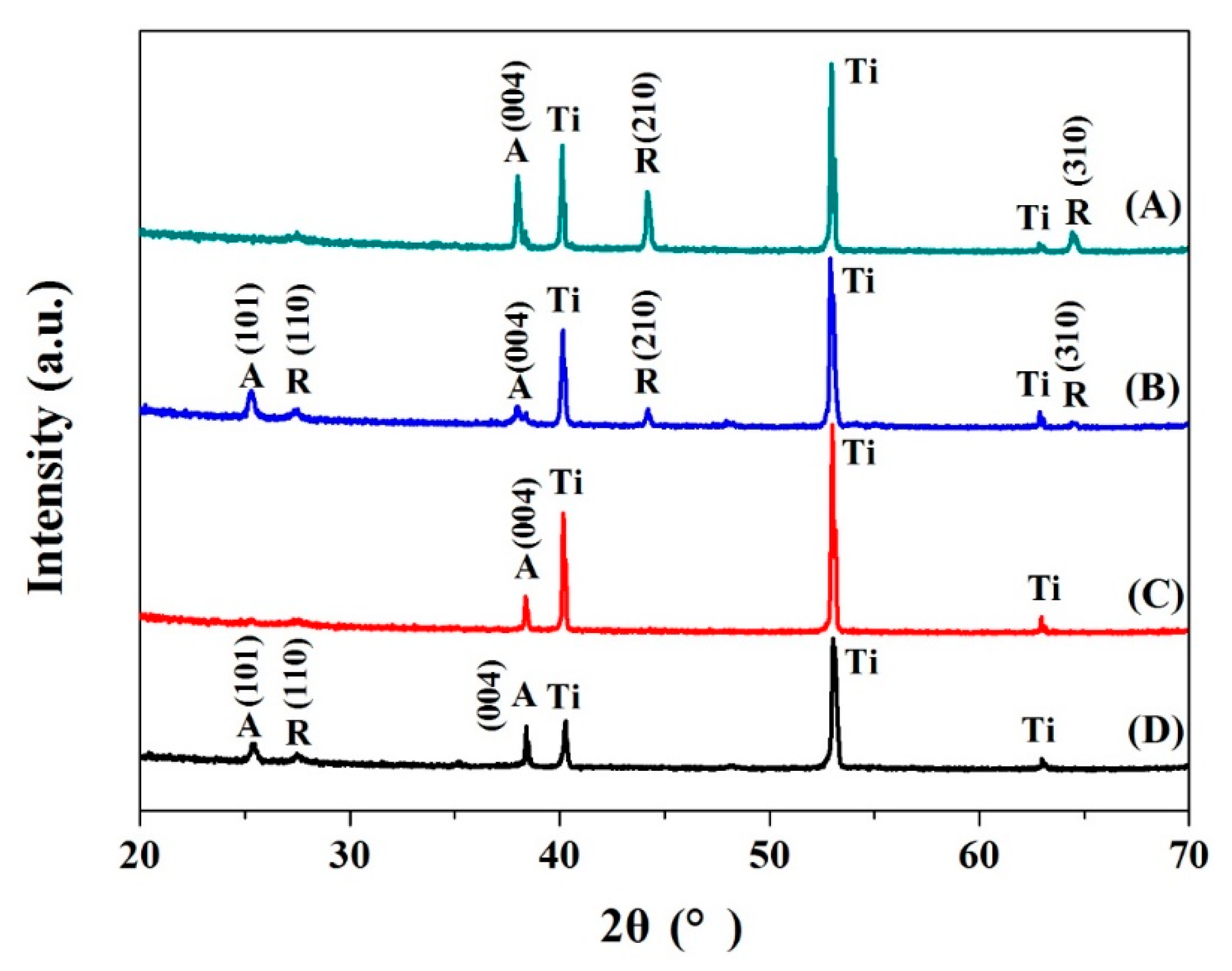
As in
Figure 3, all diffraction peaks in the X-ray diffraction (XRD, D8 Advance, Bruker, Ricoh, Japan) spectra were ascribed to TiO
2 and the Ti substrate [
23], indicating that the fabricated TiO
2 nanotube film were relatively thin and the Ti–Mo nanotubes film was intensely bonded to the substrate. After annealing treatment, TiO
2 and Mo-doped TiO
2 samples appeared at positions of 25.3°, 37.9°, and 38.9° corresponding to the anatase TiO
2 (101), (004), and (112) crystal plane diffraction peaks. The XRD peaks at 2θ = 27.6° (110) were often taken as the characteristic peaks of rutile crystal phase [
7,
25]. When the Mo doping content is reduced from 1.0% to 0%, the number of diffraction peaks of the film changes relatively, among which the film with Mo content of 0.5% shows the largest number of characteristic peaks appearing at the position of 27.5°, 44.2°, and 64.3°, corresponding to the rutile phases (110), (210), and (310), as well as the position of the 25.2° and 37.9° corresponding to anatase phase (101) and (004), respectively [
25]. In numerical terms, the ionic radius of Ti
4+ (0.068 nm) is very close to the ionic radius of Mo
6+ (0.062 nm), and when the amount of doping is not too high (0.5 at.%), most of Mo
6+ ions replace Ti
4+ as substitutional impurities. In the case of heavy doping (1.0 at.%), excess Mo enters the lattice only in the form of interstitial atoms, which aggravates the lattice deformation and suppresses grain growth [
26]. Some researchers suggest that the doping of Mo inhibits growth of crystals due to induced structure defects and hinders the transformation from anatase to rutile of TiO
2 at the same time [
7,
27].
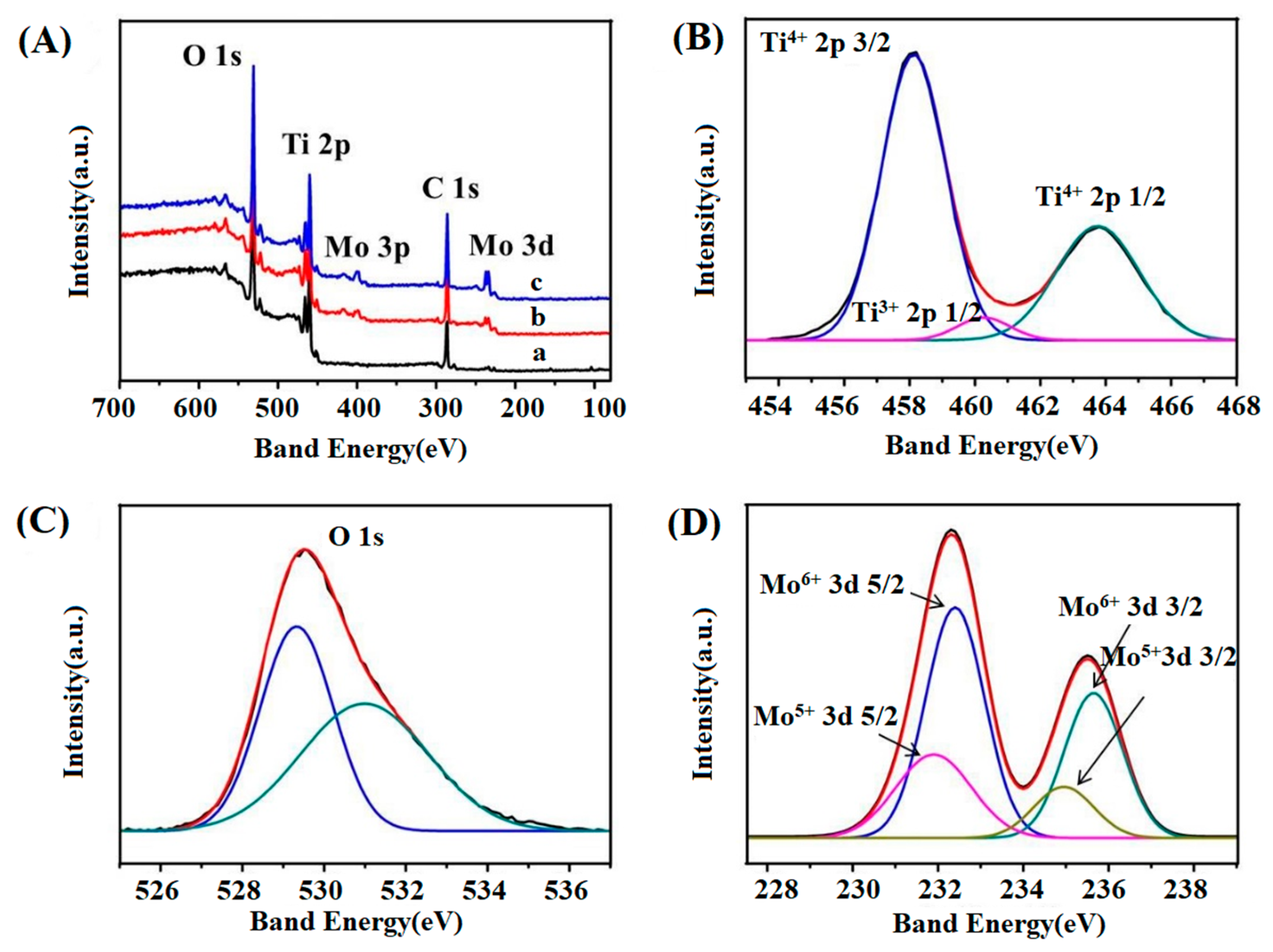
The XPS (PHI-5000C, Perkin Elmer, Hyman, Germany) survey spectra of TiO
2 and Mo-TiO
2 nanotube arrays were measured.
Figure 4A presents the full-scale XPS spectra of the TiO
2 (curve a) and Mo-TiO
2 nanotube arrays (curve b and c). The electron binding energies of all elements were calibrated against the contaminated C 1
s level (284.6 eV). The existence of the peaks of C 1
s, O 1
s, and Ti 2
p can be recognized in all samples, whereas the signature peaks of Mo emerged in the Mo-doped TiO
2 nanotube arrays. The peak of C 1
s at 284.6 eV may be due to carbon contamination in the air or carbon introduced during sample preparation. With the elevation of Mo doping concentration, the intensity of the characteristic peak of Mo is gradually increased, indicating increased Mo doping into the TiO
2 crystal lattice, which is consistent with the XRD results. From
Figure 4B, the characteristic peaks of Ti 2
p3/2 and Ti 2
p1/2 of 0.5 at.% Mo-doped TiO
2 are located at 458.2 and 463.9 eV, respectively, demonstrating the presence of Ti
4+ in the crystal. A new Ti 2
p peak appears at 460.1 eV, which can be attributed to the small amount of Ti
3+ present in TiO
2 [
28].
Figure 4C shows the O 1
s XPS spectrum of 0.5 at.% Mo-doped TiO
2, which can be divided into two peaks. The higher peak at 529.4 eV is due to O
2− in the TiO
2 lattice, and the lower peak at 531.3 eV is attributed to the surface hydroxyl group or adsorbed oxygen [
7,
21]. Hydroxyl groups help photodegradation reactions for acting as compound adsorption sites and traps of photogenerated holes producing hydroxyl radicals, which decompose organics directly [
19].
Mo 3
d3/2 and 3
d5/2 peaks of the 0.5 at.% Mo-doped TiO
2 sample are presented in
Figure 4D. It can be seen that the peaks observed at 232.5 and 235.7 eV are Mo 3
d5/2 and Mo 3
d3/2 of Mo
6+, while the peaks at 231.9 and 235.0 eV are Mo 3
d5/2 and Mo 3
d3/2 of Mo
5+ [
29]. These characteristic peaks are attributed to Mo–O bonds, revealing the successful incorporation of Mo into the TiO
2 lattice. Obtaining from the ratio of peak area, the atomic proportion of Mo
6+ and Mo
5+ would be 72.6% and 27.4%. This indicates Mo
6+ is the main dopant form in TiO
2 crystals while Mo
6+ can improve the electronic conductivity of TiO
2 photoanode [
21], which would be beneficial to the electrochemical properties of the Mo-doped TiO
2 anodes in this work.
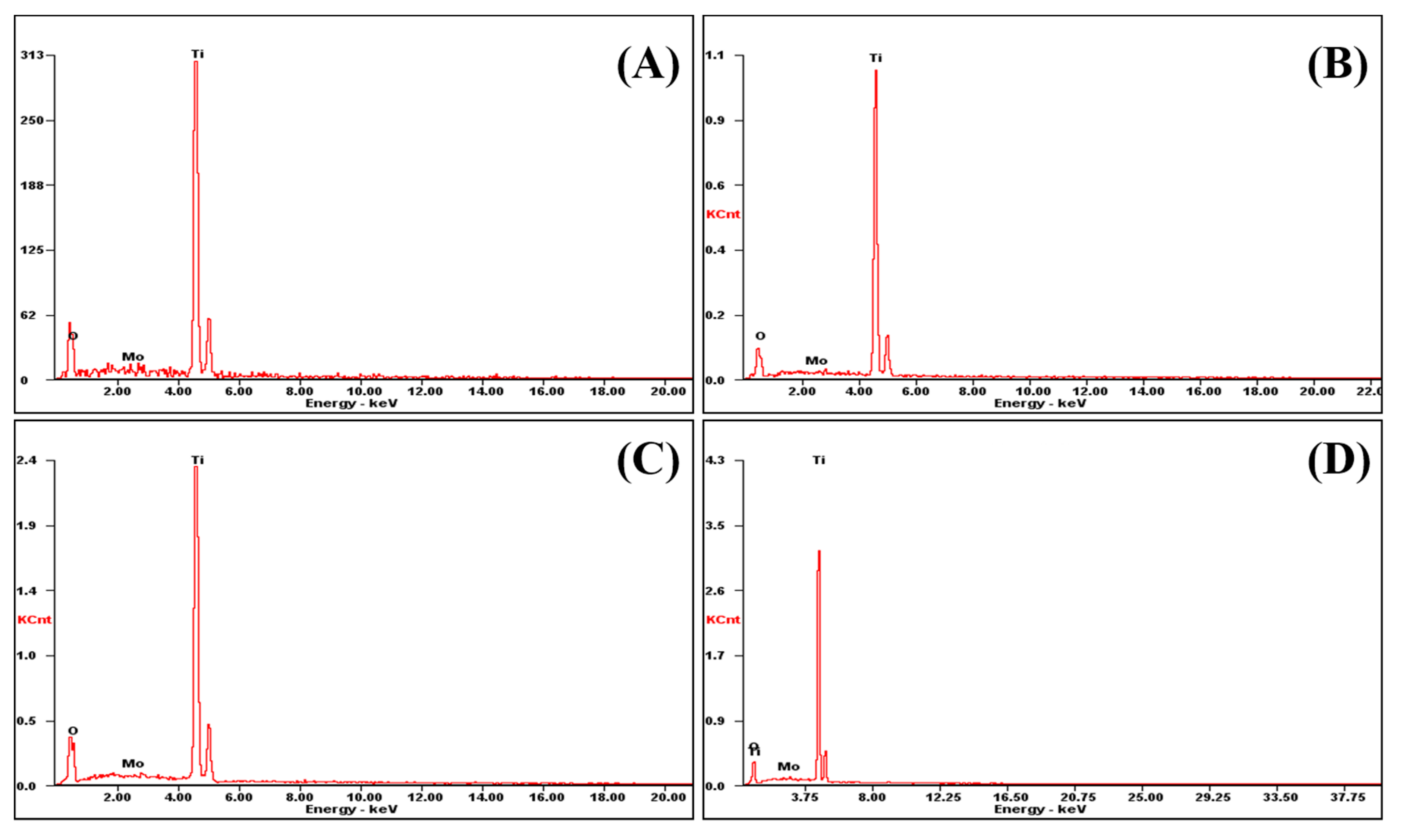
The elemental composition of the nanotube array film can be analyzed by X-ray energy spectroscopy (EDS, XL30FEG, Philips, Eindhoven, The Netherlands).
Figure 5A–D shows the EDS spectra of TiO
2 with Mo doping contents of 1.0%, 0.50%, 0.25%, and 0%, respectively. Since the film sample for the EDS test is based on Ti metal sheet with an abundant number of Ti atoms in the test area, the EDS spectrum of all test samples include a strong Ti characteristic excitation energy peak at 4.51 keV. The peak simultaneously appearing at 0.523 keV is caused by the transition of the L-layer electrons to the K-layer in the O atom, providing further proof of the Ti–O atomic composition as TiO
2. In addition, the Mo characteristic peaks with different intensities appear at 2.29 keV correspond to the X-rays energy radiating from the M-layer electrons transmitting to the L-layer in the Mo atom.
In order to calibrate the atomic percentage of Mo atoms in the TiO
2 nanotubes, the percentage of Mo atoms in the TiO
2 nanotube array film can be calculated based on the O atomic percentage. The calculated data by this method are shown in
Table 1. As shown in the figure, the four samples, Mo1.0, Mo0.5, Mo0.25, and Mo0, corresponding to the test Mo doping contents are 0.64%, 0.31%, 0.16%, and 0%. Meanwhile, the percentage of Mo atoms in Mo1.0, Mo0.5, and Mo0.25 samples are 0.99%, 0.47%, and 0.22% based on EDS analysis and calibration calculation (calculated by TiO
2 stoichiometry based on O atomic percentage), which is close to the theoretical doping content.
The specific calibration calculation mentioned above is carried out by listed equations, where we define the content of Ti accounting for half of the content of O as the atom ratio of TiO
2 since the testing result of Ti content deviates from the accurate measurement due to the extra Titanium from the substrate:
where
represents the content of Ti calculated by the ideal atomic ratio of TiO
2,
CO is original content data of O, and
CMo is original content of Mo.
CMo,calibrated,
CO,calibrated and
CTi,calibrated are the calibrated data after calculation.
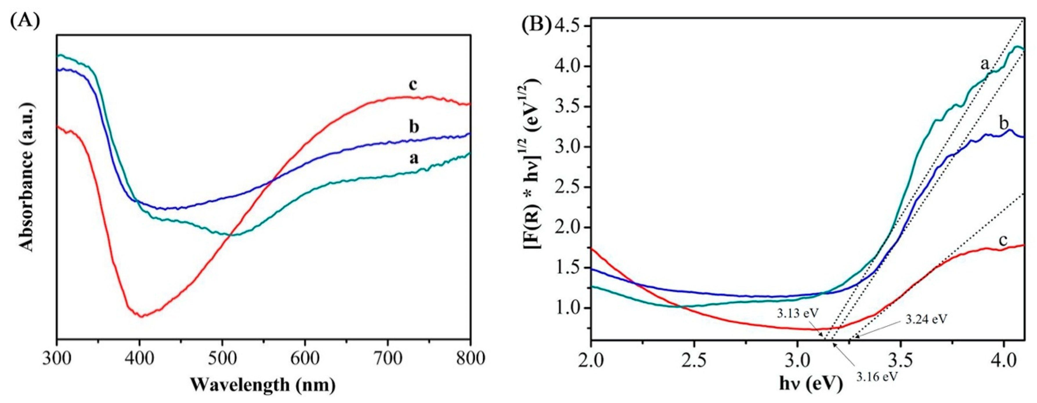
UV-visible diffuse reflectance spectroscopy (UV-Vis DRS) was performed to study the light response abilities of the TiO
2 and Mo-doped TiO
2 nanotube arrays. Shown in
Figure 6 are the UV-Vis DRS curves (A) and Tauc plots (B) of the nanotube samples with different Mo doping contents of 1.0% (a), 0.50% (b), and 0% (c). In general, the UV absorbance of nanotubes and the redshift of absorption edge intensified with the increase of Mo dopant concentration. However, in visible light range (λ = 380–780 nm), the light absorption integral area changes with an initial climb in nanotube array film followed by a decrease as the heavier Mo doping, probably due to the excessive Mo doping content, causing the destruction of nanotubes and the reduction in the arrangement density of the nanotubes, reducing the specific surface area of the whole nanotube array film, and resulting in a decrease in light absorption. Theoretically, by offering more valence electrons easily photo-incited and converting to free carriers, Mo doping with low concentration introduces a donor level below the conduction band of TiO
2, resulting in a narrower band gap [
7]. The shifted band gap can be evaluated from the absorption spectrum by the Tauc method [
26,
30]. The estimated band gap of undoped TiO
2 is 3.24 eV, agreeing with the typical value of intrinsic pure TiO
2 [
20]. Sample Mo0.5 induces a distinct bang gap drop to 3.16 eV, i.e., hence the light response wavelength moves to UV and visible light region (~392 nm). When the Mo doping content increased from 0.5% to 1.0%, the band gap decreased from 3.16 to 3.13 eV, which corresponded to the same slight redshift as well. Above all, it is notable that, for 0.5 at.% Mo-TiO
2, the light response to both UV and visible irradiation are consistently more sensitive among other doping contents. Therefore, it can be concluded that band-gap engineering could be effectively performed by searching an appropriate doping amount of Mo-TiO
2 nanotube arrays. The effective red shift of absorption band gap and the evidently enhanced light absorption under UV-visible irradiation are beneficial to the photoelectrochemical efficiency of Mo-TiO
2 nanotube arrays.
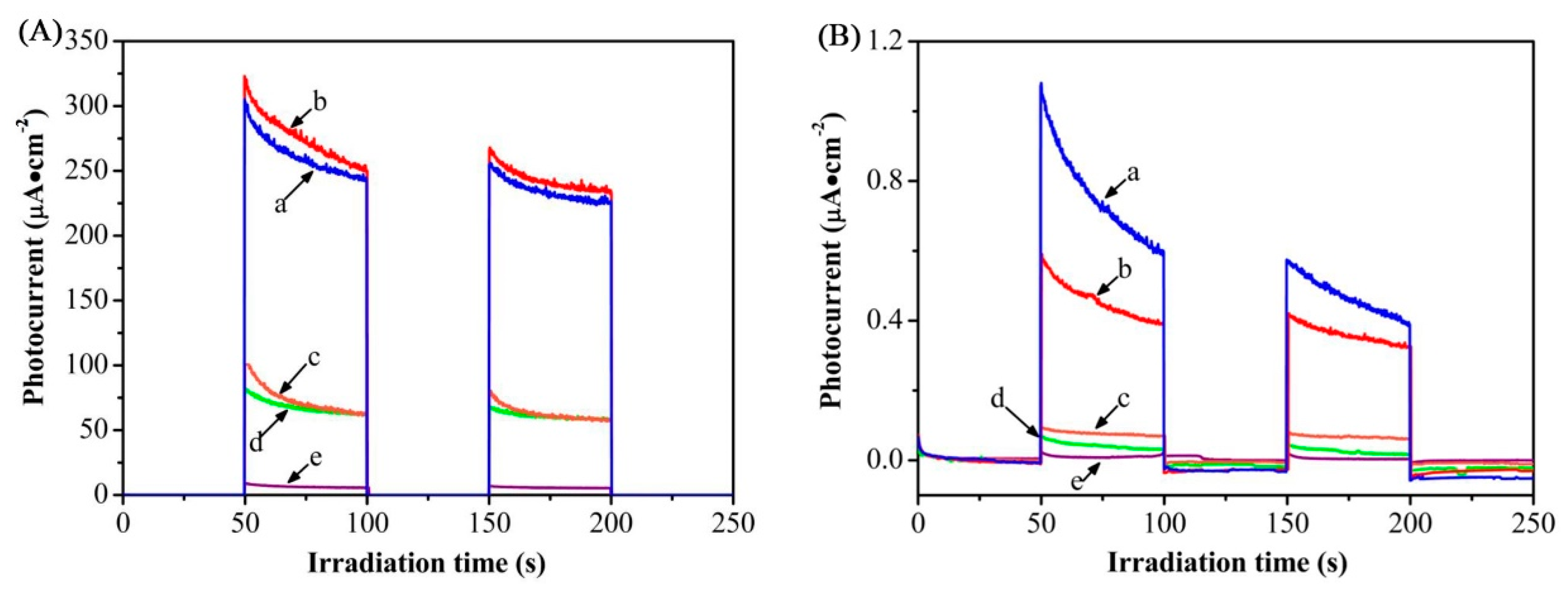
So as to further study the photoelectrochemical performance, the test was carried out in a dark manner (obscuring the xenon lamp) with the xenon lamp illuminating the sample at intervals, and a standard three-electrode electrochemical cell with Pt wire as counter electrode, saturated calomel electrode (SCE) as reference electrode, as well as TiO
2 and Mo-doped TiO
2 nanotube arrays as working electrodes were set for the photoelectrochemical measurements. Notably, the photocurrent responses to illumination were prompt in all the samples, as shown in
Figure 7. When the doping concentration of Mo reaches 0.5 at.%, the transient photocurrents of Mo-doped TiO
2 nanotubes under visible and ultraviolet visible light were 0.45 and 237.7 μA·cm
−2, respectively. Compared with TiO
2 nanotube arrays electrode (curve a), the photocurrents for 0.5 at.% Mo-doped TiO
2 nanotube arrays electrode (curve b)increased 5.8 and 4.1 times, respectively, as shown in
Figure 7A,B. Furthermore, as the doping concentration increases, the photocurrent density initially rises rapidly followed by a drop due to the distortion and imperfections of the lattice. We report that when the doping content of Mo is 0.5 at.%, the photocurrent density of the film under UV-visible light reaches maximum, and the photocurrent density under visible light is relatively enhanced and stable. The enhanced photoelectrochemical performance of Mo-TiO
2 nanotube arrays could be attributed to the synergistic effect between Mo
6+ ions and the narrowed band gap by Mo-doping. Mo
6+ ions replacing Ti
4+ in the lattice act as electron traps to promote the separation of photogenerated carriers [
20]. Meanwhile, according to the analysis of XPS, there should be surface hydroxyl groups or adsorbed oxygen (oxygen vacancies) on the surface of Mo-doped TiO
2, which may trap the photoexcited electrons to increase the separation efficiency of electron-hole pairs [
24]. However, as the content of Mo continued to rise, the photoelectrochemical performance degraded, resulting from a severe recombination rate caused by excessive lattice impurities as recombination centers. Also, the design of nanotubular structure combing with Mo-doping undoubtedly induces significant progress in photocurrent intensity.


