


Abstract
This Special Issue is devoted on design and application of thin films and structures with special emphasis on optical applications. It comprises ten papers, five featured and five regular papers, authored by respective scientists all over the world. Diverse materials are studied and their possible applications are demonstrated and discussed: transparent conductive coatings and structures from ZnO doped with Al and Ga and Ti-doped SnO2, polymer and nanosized zeolite thin films for optical sensing, TiO2 with linear and non-linear optical properties, organic diamagnetic materials, broadband optical coatings, CrWN glass molding coatings and silicon on insulator waveguides.
1. Introduction
Diverse types of materials such as polymers, glasses, metals, ceramics, zeolites, etc., could be prepared as thin films with high optical quality thus finding applications in photonics, optical sensing, photocatalysis, optoelectronics, linear and non-linear optics, holography, etc. Different production strategies, including “dry” and “wet” deposition methods, are developed and optimized. In order for these thin films and structures to be utilized in different optical devices, unambiguous methods for design and characterization are required. Additionally, in-situ optical monitoring of their properties will be beneficial for proper device operation.
This Special Issue covers the recent progress and new developments in the area of design, deposition, characterization and application of optical thin films and structures.
2. Statistics of the Special Issue
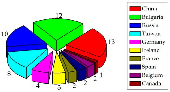
The special issue consists of 10 full papers authored by 57 authors. The geographical distribution of authors can be seen in Figure 1. The authors originate from 10 countries from three different continents—Europe, Asia and North America. The average number of authors per manuscript is 5.7.
Figure 1.
Geographic distribution by the country of authors.
3. Brief Overview of the Contributions to This Special Issue
Tikhonravov et al. [1] presented a computational approach for comparing various broadband monitoring strategies, taking into account the positive and negative effects associated with the correlation of thickness errors caused by the monitoring procedure. The presented computational approach is general and can be applied to check the prospects of the production of various types of optical coatings. Stenzel et al. [2] studied linear and non-linear optical properties of titanium dioxide films prepared by plasma ion-assisted electron beam evaporation. Linear optical properties were investigated in terms of spectrophotometry using the beta-distributed oscillator model as a parametrized dispersion law. The nonlinear two-photon absorption coefficient of titanium dioxide was determined by means of the laser-induced deflection technique at a wavelength of 800 nm. Dimitrov et al. [3] demonstrated transparent and conductive aluminum-doped zinc oxide (AZO) thin films deposited on rigid and transparent substrates through atomic layer deposition. Applications as transparent conductive layers in AZO/glass-supported liquid crystal displays and flexible polymer-dispersed liquid crystal devices were discussed. Akhmedov et al. [4] investigated the structural, electrical, and optical performances of Ga-doped ZnO/Ag/Ga-doped ZnO (GZO/Ag/GZO) multilayered structures deposited on glass substrates by direct current (DC) magnetron sputtering in a pure Argon medium without any substrate heating. Highly transparent and conductive samples were obtained. Liu et al. [5] investigated Ti-doped SnO2 transparent conductive oxide thin films deposited on glass substrates using radio frequency (RF) magnetron sputtering and postdeposition annealing at temperatures in the range of 200–500 °C for 30 min. The effects of the annealing temperature on the structural properties, surface roughness, electrical properties, and optical transmittance of the thin films are then systematically explored. Cody et al. [6] demonstrated a possibility of optical sensing of copper ions in water using Linde Type L (LTL) zeolite thin films. Both single wavelength and spectroscopic ellipsometry were used for characterization of the changes in optical constants and thickness of films in the presence of heavy metal ions. Lazarova et al. [7] demonstrated a possible approach for enhancement of Poly(vinyl alcohol) (PVA) humidity-sensing ability using poly(vinylalcohol-co-vinylacetal) copolymers of different acetal content. Further enhancement through preparation of polymer–silica hybrids was demonstrated. The possibility of color sensing of humidity was also discussed. Eerdekens et al. [8] demonstrated organic, diamagnetic materials based on structurally simple (hetero-)tolane derivatives that form crystalline thin-film aggregates suitable for Faraday rotation spectroscopy. Huang at al. [9] studied the impact of vacuum annealing on CrWN glass molding coatings deposited by plasma enhanced magnetron sputtering. The vacuum annealing induced surface coarsening and spinodal decomposition accompanied by the formation of nm-sized c-CrN, c-W2N, and h-WN domains. The large volume fraction of the last one seriously weakened the coating strength and caused a drop in hardness. Shang et al. [10] used a theoretical/experimental combinative model for investigation of the waveguide sidewall roughness (SWR) and its impact on the optical propagation losses in silicon-on-insulator waveguides.
4. Conclusions
In making this Special Issue on Optical Thin Films and Structures: Design and Advanced Applications, I had the pleasure of communicating with first-class authors worldwide and the chance to obtain high quality contributions. I am very grateful to all the authors of the Special Issue for their submissions. I hope that the papers will be useful and of interest for the readers.
Conflicts of Interest
The author declares no conflict of interest.
References
- Tikhonravov, A.; Kochikov, I.; Matvienko, I.; Isaev, T.; Yagola, A. Strategies of broadband monitoring aimed at minimizing deposition errors. Coatings 2019, 9, 809. [Google Scholar] [CrossRef] [Scilit]
- Stenzel, O.; Wilbrandt, S.; Mühlig, C.; Schröder, S. Linear and nonlinear absorption of titanium dioxide films produced by plasma ion-assisted electron beam evaporation: Modeling and experiments. Coatings 2020, 10, 59. [Google Scholar] [CrossRef] [Scilit]
- Dimitrov, D.; Tsai, C.-L.; Petrov, S.; Marinova, V.; Petrova, D.; Napoleonov, B.; Blagoev, B.; Strijkova, V.; Hsu, K.Y.; Lin, S.H. Atomic Layer-Deposited Al-Doped ZnO Thin Films for Display Applications. Coatings 2020, 10, 539. [Google Scholar] [CrossRef] [Scilit]
- Akhmedov, A.K.; Abduev, A.K.; Kanevsky, V.M.; Muslimov, A.E.; Asvarov, A.S. Low-temperature fabrication of high-performance and stable GZO/Ag/GZO multilayer structures for transparent electrode applications. Coatings 2020, 10, 269. [Google Scholar] [CrossRef] [Scilit]
- Liu, C.-F.; Kuo, C.-H.; Chen, T.-H.; Huang, Y.-S. Optoelectronic properties of Ti-doped SnO2 thin films processed under different annealing temperatures. Coatings 2020, 10, 394. [Google Scholar] [CrossRef] [Scilit]
- Cody, D.; Babeva, T.; Madjarova, V.; Kharchenko, A.; Gul, S.; Mintova, S.; Barrett, C.J.; Naydenova, I. In-situ ellipsometric study of the optical properties of LTL-doped thin film sensors for Copper(II) ion detection. Coatings 2020, 10, 423. [Google Scholar] [CrossRef] [Scilit]
- Lazarova, K.; Bozhilova, S.; Novakov, C.; Christova, D.; Babeva, T. Amphiphilic Poly(vinyl Alcohol) copolymers designed for optical sensor applications—synthesis and properties. Coatings 2020, 10, 460. [Google Scholar] [CrossRef] [Scilit]
- Eerdekens, M.; López-Duarte, I.; Hennrich, G.; Verbiest, T. Thin films of tolane aggregates for Faraday rotation: Materials and measurement. Coatings 2019, 9, 669. [Google Scholar] [CrossRef] [Scilit]
- Huang, X.; Xie, Z.; Li, K.; Chen, Q.; Chen, Y.; Gong, F. Thermal stability of CrWN glass molding coatings after vacuum annealing. Coatings 2020, 10, 198. [Google Scholar] [CrossRef] [Scilit]
- Shang, H.; Sun, D.; Yu, P.; Wang, B.; Yu, T.; Li, T.; Jiang, H. Investigation for sidewall roughness caused optical scattering loss of silicon-on-insulator waveguides with confocal laser scanning microscopy. Coatings 2020, 10, 236. [Google Scholar] [CrossRef] [Scilit]
Publisher’s Note: MDPI stays neutral with regard to jurisdictional claims in published maps and institutional affiliations. |
© 2020 by the author. Licensee MDPI, Basel, Switzerland. This article is an open access article distributed under the terms and conditions of the Creative Commons Attribution (CC BY) license (http://creativecommons.org/licenses/by/4.0/).