Abstract
In this study, zinc is anodized at different voltages in 0.1 mol·dm−3 KOH electrolyte to form nanoporous anodic films. Dark-colored anodic films are formed at anodizing voltages ≤6 V, whereas colorless anodic films are developed at voltages ≥7 V. The anodic films formed at all voltages consist of crystalline ZnO, which was identified by X-ray diffraction and Raman spectroscopy. The Raman spectra of the dark-colored anodic films show the enhanced intensity of the LO phonon mode due to electric-field-induced Raman scattering, which may be associated with the presence of metallic Zn nanoparticles in the anodic films. Scanning electron micrographs and transmission electron micrographs of the cross-section of the dark-colored anodized zinc reveal the formation of two-layer porous anodic films with a highly rough metal/film interface. In contrast, nanoporous anodic films of uniform thickness with a relatively flat metal/film interface are formed for the colorless anodized zinc. The transmission electron microscopy (TEM)/energy dispersive X-ray spectroscopy (EDS) analysis suggested the presence of zinc nanoparticles in the dark-colored anodic films. The non-uniform anodizing and the formation of metal-nanoparticle-dispersed porous anodic films cause the formation of dark-colored anodic films on zinc.
1. Introduction
Anodizing is an electrochemical process that forms nanostructured oxide surface films on a range of metals. A typical and well-known example is the formation of self-ordered porous anodic films on aluminum [1,2]. Anodized aluminum and aluminum alloys have been widely used for corrosion protection, wear resistance, and decoration of surfaces [3,4]. In the last two decades, nanotubular anodic films formed on titanium have been extensively investigated for the fundamental understanding of the evolution mechanism of nanotube morphology and for many promising applications, including photocatalysis, solar cells, self-cleaning, and biomedical implants [5,6,7]. Anodizing techniques to form nanostructured surfaces have been extended to a range of metals in the last two decades, such as iron [8,9,10], cobalt [11], nickel [12,13], zinc [14], zirconium [15], niobium [16], and tantalum [17]. Utilizing organic electrolytes such as ethylene glycol and glycerol, containing fluoride and a small amount of water is one of the keys to form thick self-ordered nanoporous or nanotubular anodic films on a wide range of metals. The anodic films formed in such fluoride-containing organic electrolytes often consist of oxyfluoride or fluoride; however, those can be converted to chemically stable oxides by thermal treatment, mostly in air atmosphere.
The growth of the self-ordered porous anodic films is associated with the field-assisted flow of the film material from the pore base to the pore wall [18,19,20]. The stress generated due to the film growth induces the flow of the film material [21,22]. However, the growth mechanism is dependent on the anodizing conditions, particularly, the anodizing electrolyte [23]. It was reported that the field-assisted flow is predominant for the porous anodic film growth on aluminum in sulfuric acid, oxalic acid, and phosphoric acid [20,24], whereas a field-assisted dissolution mechanism is predominant for the formation of porous anodic films in chromic acid and borax electrolytes [25,26]. Thus, the anodizing electrolyte plays an important role in the growth of porous anodic films.
Zinc has been anodized in several electrolytes. The porous anodic films were formed on zinc in an oxalic acid electrolyte [27,28]. The porous ZnO films showed superior performance as a methane sensor [27,29]. The formation of nanoporous anodic ZnO films was also reported in NaOH electrolytes [30,31]. In addition to nanoporous structures, several nanostructured anodic films have been reported. For instance, self-assembled stripe arrays of zinc oxide were developed in an ethanolic H2SO4 electrolyte [32]. ZnO films consisting of bundles of nanowires were obtained in an NH4F electrolyte. He et al. reported the variation of the nanostructures of the anodic films, such as nanodots, nanowires, and nanoflowers, formed on zinc in ethanol–water mixed electrolytes containing HF, depending on the electrolyte composition and anodizing voltage. The electrolytes of bicarbonate are useful for forming anodic nanowire films on zinc [33,34,35,36,37,38,39,40]. The as-anodized nanowires are composed of basic zinc carbonate; however, they can be converted to crystalline ZnO after annealing above 200 °C [33]. ZnO is a widegap n-type semiconductor and has many promising applications, including in photocatalysis, sensors, and solar cells. Thus, anodizing is a simple and cost-effective process to form nanostructured ZnO surface films on zinc and zinc-coated steels for many potential and specific applications.
The color of anodized metals is of interest for practical applications. In fact, the coloring of anodized aluminum and its alloys has been commercially utilized. Recently, dark coloring of zinc was reported by anodizing in alkaline electrolytes such as Na2CO3 or NaOH [41,42]. The oxide formed was crystalline ZnO, and ZnO is known to be transparent. Thus, the mechanism of the coloring of anodized zinc is still unclear. Since zinc has been widely used as zinc-coated steels, the coloring of zinc is of practical importance for decoration. In addition, unusual dark coloring by anodizing of zinc is of scientific interest. In the present study, zinc was anodized at various voltages in 0.1 mol·dm−3 KOH electrolyte to determine the anodizing conditions for coloring. The colored anodized zinc specimens were characterized using scanning electron microscopy (SEM), scanning transmission electron microscopy (STEM)-energy-dispersive X-ray spectroscopy (EDS), X-ray diffraction (XRD), and Raman spectroscopy. The coloring mechanism is discussed based on the characterization results.
2. Materials and Methods
A high-purity (99.99%) zinc plate (Nilaco Corporation, Tokyo, Japan) of 1.0 mm thickness was used in this study. Prior to anodizing, the zinc plate was electropolished at 20 V in 30 vol% H3PO4-ethanol electrolyte at <5 °C for 5 min. The electropolished zinc plate was anodized at several voltages between 3 and 15 V in 0.1 mol·dm−3 KOH electrolyte at 25 °C for 30 min. A two-electrode cell with a Pt counter electrode was used for anodizing, and a constant voltage was applied using a DC power supply (Kikusui Electronics, Kanagawa, Japan, PAS-80-9). The current transient was monitored using a digital multimeter (Agilent Technologies, Santa Clara, CA, USA, 34460A) and recorded on a PC using a software (Agilent Technologies, Santa Clara, CA, USA, Agilent VEE Pro). After anodizing, the anodized specimen was washed with Milli-Q water and dried in the air.
The surface and cross-section of the anodized specimens were observed using a field-emission scanning electron microscope (Zeiss, Jena, Germany, Sigma-500), operated at 1.5 kV, with Everhart–Thornley and in-lens secondary electron (SE) and backscattered electron (BSE) detectors. Furthermore, the cross-section of the specimens was observed using an atom-resolution scanning transmission electron microscope (JEOL, Tokyo, Japan, JEM-ARM200F) equipped with EDS facilities and operated at 200 kV. The electron-transparent sections were prepared using an ultramicrotomy technique.
Phases in the anodized specimens were identified by X-ray diffraction measurements (Rigaku, Tokyo, Japan, RINT-2200) with Cu Kα radiation (λ = 0.15418 nm) in the α-2θ mode (α = 2°). The Raman spectra of the anodized specimens were also measured using a 532-nm laser (Horiba, Tokyo, Japan, XploRA).
3. Results and Discussion
3.1. Anodizing Characteristics
Figure 1a shows the current transients of zinc during anodizing at different voltages in the KOH electrolyte for 30 min. At voltages ≤6 V, a relatively small change in current was observed after anodizing for 300 s. However, the current decreased gradually at voltages ≥7 V. The steady-state current density increased with increasing anodizing voltage up to 6 V; however, for anodizing voltages ≥7 V, the final current densities after anodizing for 30 min were similar. Thus, the current transients changed between 6 and 7 V. The voltage dependence of the final current density is plotted in Figure 1b. The i–V curve shows an active–passive transition-type behavior, and the current peak appears at 6 V, above which the current density is significantly reduced and became almost voltage -independent. In anodizing of aluminum, the voltage dependence of the anodizing current density changes with the anodizing electrolyte [43]. For instance, the current density increases with increasing the anodizing voltage in sulfuric acid and oxalic acid electrolytes, in which self-ordered nanoporous anodic alumina films are developed [20,24]. In contrast, an almost steady-state current is observed in a wide range of anodizing voltages in chromic acid, borax, and ammonium pentaborate electrolytes, in which a less-ordered porous structure is developed [25,26]. The two different voltage dependencies of the current may be related to the mechanism of film growth because the field-assisted flow is observed in sulfuric acid and oxalic acid, whereas the field-assisted dissolution mechanism for porous film formation or barrier-type film growth is predominant in the latter electrolytes. In the present anodizing of zinc in KOH electrolyte, it is likely that the growth mechanism may change at anodizing voltages between 6 and 7 V. In correlation with this, the color of the anodized zinc is also dependent on the anodizing voltage; dark-colored specimens were obtained up to 6 V, whereas the specimens anodized at voltages ≥7 V were practically colorless (Figure 1c).
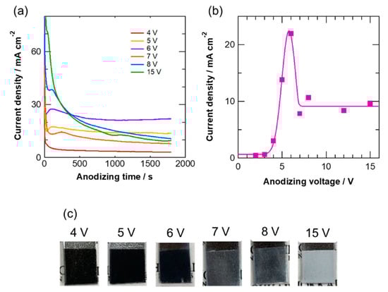
Figure 1.
(a) Current transients of zinc during anodizing at different voltages in 0.1 mol·dm−3 KOH electrolyte at 20 °C for 30 min, (b) change in the final current density with anodizing voltage, and (c) digital camera images of the specimens anodized at several voltages for 30 min.
3.2. Characterization of the Anodic Films
The anodic films formed at all voltages are crystalline. The XRD patterns of the anodized specimens (Figure 2a) reveal reflections corresponding to wurtzite-type ZnO. The reflections of the zinc substrate were also observed for all the specimens; however, their intensities were significantly reduced at voltages ≥7 V, as a consequence of the formation of thick anodic films at such high voltages, which was confirmed by the cross-section observations. The changes in the grain size and the lattice spacing of the (002) plane of ZnO with respect to the anodizing voltage are summarized in Table 1. The size of the ZnO crystals decreased with increasing anodizing voltage, particularly above 6 V; however, the (002) lattice spacing remained almost unchanged at all anodizing voltages. It was reported that the lattice parameter c increases slightly with the introduction of oxygen vacancies [44]. It has been often discussed that the introduction of oxygen vacancies causes dark coloring of ZnO films [41]. The similarity of the (002) lattice spacing at all anodizing voltages in this study suggests the little introduction of oxygen vacancies in the anodic films on zinc. Thus, dark coloring may not be related to the introduction of oxygen vacancies in the present study.
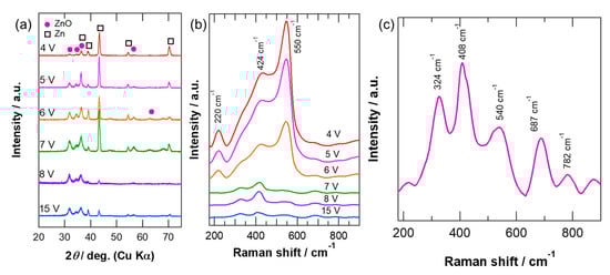
Figure 2.
(a) X-ray diffraction (XRD) patterns and (b) Raman spectra of zinc anodized at different voltages in 0.1 mol·dm−3 KOH electrolyte at 20 °C for 30 min, and (c) enlarged Raman spectrum of zinc anodized at 15 V.

Table 1.
Changes in the size of the ZnO crystallite and the (002) lattice spacing of ZnO with anodizing voltage.
Raman spectroscopy was also utilized to obtain the structural information of the anodic films. Figure 2b shows the Raman spectra of the zinc specimens anodized at different voltages. All the observed peaks are assigned to wurtzite-type ZnO; however, the relative intensity of each peak changes between 6 and 7 V. The most intense peak at 550 cm−1 for the specimens anodized at voltages up to 6 V is assigned to the band of the LO mode of ZnO, and the peak at 410 cm−1 is the E1(TO) band [44]. The peak at ~220 cm−1 appears for specimens anodized at voltages up to 6 V, which is the overtone of the E2low mode. This peak was not detected clearly at voltages ≥7 V. A shoulder peak at ~320 cm−1 is the combination of E2high–E2low [44]. The Raman peak intensities were significantly reduced at voltages ≥7 V as compared to those at anodizing voltages up to 6 V. The most intense peak also changes to the E1(TO) band at 408 cm−1 (Figure 2c) at voltages ≥7 V. It has been reported that a marked enhancement of the LO band occurs when oxygen vacancies are present in ZnO [44]. The LO band was also enhanced when the ZnO/Zn composite films were developed by the incomplete oxidation of zinc [45]. The Zn/ZnO core–shell nanoparticles also showed enhanced LO band intensity [46]. The results of the XRD patterns (Table 1) indicate a small change in the lattice spacing with respect to the anodizing voltage; therefore, it is likely that the enhanced LO bands of the Raman spectra obtained at voltages ≤6 V may be associated to the presence of the metallic zinc in the anodic films, not by the introduction of oxygen vacancies.
The film morphology was examined using surface SEM. Figure 3 shows scanning electron micrographs of the surface of anodized zinc at different voltages. Granular porous films are formed at voltages ≤6 V and the size of the particles is 15–40 nm. Anodic films with lower porosity and smaller particle size were obtained at anodizing voltages ≥7 V. Figure S1 shows the change in the surface morphology with respect to anodizing time at an anodizing voltage of 5 V. A granular film is formed even at a short anodizing time of 30 s, and the size of the particles increased with time. In addition, the surface roughened with increasing anodizing time. The formation of similar granular porous films was also reported previously by anodizing of zinc in 0.1 mol·dm−3 NaOH electrolyte [31].
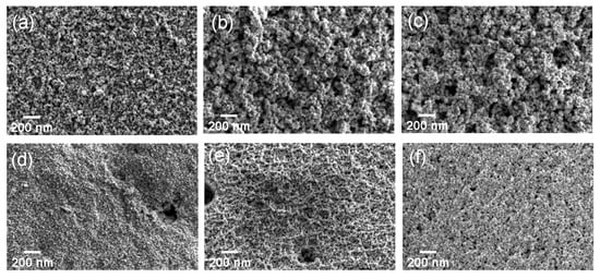
Figure 3.
Scanning electron micrographs of the surfaces of the anodic films formed on zinc at (a) 4 V, (b) 5 V, (c) 6 V, (d) 7 V, (e) 8 V, (f) 15 V.
Figure 4 shows the cross-sectional scanning electron micrographs of the anodic films formed at the anodizing voltages of 5 and 15 V for 30 min. Several characteristic differences in these two anodic films are observed. The thickness of the anodic film formed at 5 V is ~1.1 μm, which is only about one-fifth of that of the film formed at 15 V. The electric charges passed during anodizing were 26.9 and 35.0 C·cm−2 at 5 and 15 V, respectively, thus revealing a relatively small influence of the anodizing voltage on the electric charge. The formation of a thicker film at 15 V as compared to that at 5 V despite similar electric charges during anodizing indicates significantly efficient film formation at 15 V. This may be correlated with the current transients shown in Figure 1. The dissolution of zinc appears to be predominant at anodizing voltages ≤6 V, where the current density increases with the increasing anodizing voltage. In contrast, at anodizing voltages ≥7 V, the anodizing current reduced with increasing anodizing time and became almost independent of the anodizing voltage. Thickening of the barrier layer with increasing time and formation voltage probably led to such time and voltage dependence of the anodic current. The presence of such a barrier layer impedes the dissolution of zinc and promotes film formation. The lower porosity of the anodic film formed at 15 V (Figure 4e) compared to that at 5 V (Figure 4a) is also possibly related to the enhanced efficiency of film formation. Thus, thicker and less-porous anodic films are developed at 15 V in comparison with that formed at 5 V.
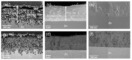
Figure 4.
(a,c,e) In-lens secondary electron (SE) and (b,d,f) backscattered electron (BSE) scanning electron micrographs of the cross-sections of the anodic films formed on zinc at (a,b) 4 V and (c–f) 15 V for 1800 s.
Another important difference is the morphology of a metal/film interface. The anodic film formed at 15 V has a flat metal/film interface (Figure 4c–f). Such an interface is often developed during anodizing of aluminum [47]. In this case, a uniform barrier layer is developed between the metal substrate and the electrolyte or a porous layer, and the uniformity of the electric field applied in the barrier layer determines the oxidation rate of the zinc substrate constant on the entire metal surface. In contrast, an unusual metal/film interface is developed at 5 V, at which the interface is rather rough, although the film surface is relatively flat (Figure 4a,b). The development of a highly rough metal/film interface is associated with the non-uniform oxidation of the zinc substrate at the interface, which may be related to the absence of a sufficient barrier in the anodic film. During the growth of both the barrier-type and porous-type anodic films on aluminum, the thickness of the barrier layer increases linearly with the anodizing voltage [48]. The rate of the film growth is controlled by the ionic transport in the barrier layer under a high electric field of 106–107 V·cm−1 [49]. In the present anodizing conditions at voltages ≤6 V, an anodic film that can uniformly sustain a high electric field may not be formed, thus leading to a local increase in the ionic current and non-uniform oxidation of the zinc substrate. The large increase in the anodic current density with the increasing anodizing voltage (≤6 V) (Figure 1b) is also another indirect evidence of the absence of a sufficient barrier in the anodic films.
Further detailed structural and compositional characterizations were performed using TEM/EDS analysis. Figure 5a shows the transmission electron micrograph of an ultramicrotomed section of zinc anodized at 5 V. Indeed, a two-layer anodic film with an outer layer having higher porosity is developed on the zinc substrate. The thickness of the outer layer is approximately 300–400 nm, and the outer layer corresponds to the region above the dashed line shown in Figure 4a. The selected-area electron diffraction (SAED) pattern revealed the presence of wurtzite ZnO (Figure 5b), which is in agreement with the Raman spectroscopy and XRD results (Figure 2). No additional phase was resolved in this region. The thickness of the remaining inner layer of the anodic film was comparable to that of the outer layer. The SAED pattern of this region (Figure 5c) revealed the presence of a metallic zinc phase in addition to the wurtzite-type ZnO. Metallic zinc nanoparticles should be dispersed in the inner layer of the anodic film formed at 5 V, showing a metallic zinc phase in the SAED pattern. Figure S2 shows the transmission electron micrograph of an ultramicrotomed section of zinc anodized at 15 V for 300 s. The short anodizing time was selected for TEM observation because the sectioning of the anodic films as thick as ~6 μm is rather difficult by ultramicrotomy. An anodic film of ~1.5 μm thickness was developed with a flat metal/film interface. A crack penetrating the metal substrate was present in the anodic film, and this may have formed during the ultramicrotomed sectioning and not during the anodizing. The film appeared to be porous, and a higher-porosity region was found in its outer part, which was possibly formed by a dissolution–precipitation mechanism, i.e., dissolution of zinc as Zn(OH)42− species followed by its precipitation as ZnO [50]. Because of the higher growth efficiency at this anodizing voltage compared to that at 5 V, the remaining inner part of the film can be directly formed at the metal/film interface, as in the case of the anodizing of aluminum in acid electrolytes. The SAED pattern shown in the inset reveals that only wurtzite-type ZnO is present in the anodic film formed at 15 V. Similar SAED patterns were obtained for the other regions of the anodic film. No metallic zinc phase was present in the anodic film formed at this voltage.
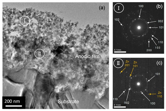
Figure 5.
(a) Transmission electron micrograph of an ultramicrotomed section of the anodic films formed on zinc at 5 V for 1800 s and selected area electron diffraction patterns of the regions (b) I and (c) II in (a).
The compositions of the anodic films formed at 5 and 15 V were also examined by EDS. The scanning transmission electron micrograph of zinc anodized at 5 V is shown in Figure 6a, and the respective zinc and oxygen elemental maps are shown in Figure 6b,c, respectively. The intensities of both zinc and oxygen in the inner layer are higher than those in the outer layer, probably reflecting the higher porosity (lower density) of the outer layer. The distribution of zinc in the anodic film, particularly in the inner layer, was not uniform, and the high-intensity regions of zinc in the inner layer appeared dark, as shown in Figure 6a. Considering the distribution of oxygen in the inner layer, the intensity of oxygen did not clearly increase in the high-intensity regions of zinc. Thus, the different distributions of zinc and oxygen in the anodic film indicate that the zinc nanoparticles, probably those mainly located in the darker regions of the anodic film shown in Figure 6a, are dispersed in the ZnO-base anodic film. In contrast, similar distributions of zinc and oxygen are observed in the anodic films formed at 15 V (Figure 6d–f). The anodic film formed at 5 V contained the dispersed zinc nanoparticles; however, the nanoparticles were not present in the film formed at 15 V. Quantitative EDS point analysis of the regions shown in Figure S3 was also performed, and the oxygen content at each square region is shown in the figure. Compared to the oxygen content in the anodic film formed at 15 V, the oxygen content in the anodic film formed at 5 V was rather low, particularly in the regions with darker appearance. Even in the outer part of the anodic film formed at 5 V, the oxygen content is low compared to that at 15 V. Thus, zinc nanoparticles may also be present in the outer part of the film formed at 5 V.
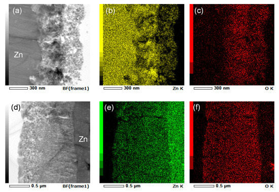
Figure 6.
(a,d) Scanning-transmission electron micrographs and respective (b,e) Zn and (c,f) O elemental maps of Zn anodized at (a–c) 5 and (d–f) 15 V.
3.3. Mechanism of Dark Coloring
Chen et al. reported the formation of colored anodic films on zinc by electrochemical treatments in the Na2CO3 electrolyte [42]. Anodically oxidized zinc showed a light-gray appearance and a much darker color was obtained after the subsequent electrochemical reduction treatment. They suggested the presence of inter-gap states that absorb visible light and influence the optical appearance. The formation of zinc nanoplates was proposed by the authors after electrochemical reduction, although this was not directly confirmed.
Recently, Mika et al. reported dark nanoporous anodic films formed on zinc in the NaOH electrolyte [41]. The dark-colored films were directly formed at 2 and 4 V. The resultant anodic films consisted of crystalline ZnO, which was highly defective with a large number of oxygen vacancies and zinc interstitials. They concluded that the dark color is associated with the existence of additional electronic states deep in the ZnO bandgap.
In the present study, nanoporous anodic films were formed at different voltages (≤15 V), and dark-colored zinc was obtained only at anodizing voltages ≤6 V. For these voltages, the current density increased with increasing anodizing voltage. Similar XRD patterns were obtained regardless of the anodizing voltage, and the (002) lattice spacing of the wurtzite ZnO was independent of the anodizing voltage (Table 1). The size of the ZnO crystallite is slightly larger at lower anodizing voltages than that at 15 V. Therefore, it is difficult to say that the coloring only at low anodizing voltages is associated with the deficiency of ZnO, because the deficiency-induced change in the lattice parameter is not observed in this study. The deficiency of ZnO has been often discussed as a reason for the dark coloring of ZnO [41], but another mechanism needs to be considered for the formation of dark-colored zinc. Significant anodizing voltage dependence is observed by SEM and TEM/EDS characterizations. A highly rough metal/film interface was developed at voltages ≤6 V in contrast to the flat interface developed at voltages ≥7 V. Metallic zinc nanoparticles dispersed in the anodic film only in the colored zinc specimen. Based on the findings of this study, we suggest that dark coloring occurs as a consequence of the dispersion of the zinc metal nanoparticles in the anodic film along with the formation of a highly rough metal/film interface. Under such a film morphology, visible light is confined within the anodic film and the dark coloring of the anodized zinc occurs.
Figure 7a shows a schematic illustration of the growth of the anodic film on zinc at voltages ≤6 V. At these anodizing voltages, non-uniform oxidation of zinc occurs, thus resulting in the roughening of the metal/film interface. A granular porous film may be formed by the dissolution of zinc as Zn(OH)42− species followed by the precipitation of ZnO [50]. The non-uniform oxidation of zinc induces the development of highly rough metal/film interface, causing the incorporation of zinc metal nanoparticles, probably at the convexity of the rough interface, into the anodic film without oxidation. In contrast, a barrier layer that can sustain a high electric field strength is formed between the metal substrate and the porous layer at voltages ≥7 V (Figure 7b), thus leading to a reduction in the current density to lower than that at 6 V, although the barrier layer was not directly observed by SEM and TEM. Because of the presence of the barrier layer, a flat metal/film interface was developed and the film-formation efficiency was significantly enhanced. Thus, a major part of the porous layer may be formed directly without the dissolution of zinc species. Only the outer part of the film with higher porosity is likely to be formed by the dissolution/precipitation mechanism.
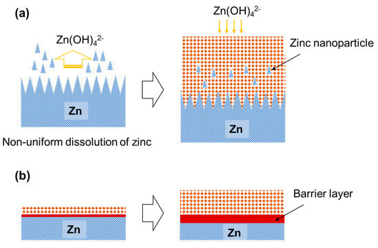
Figure 7.
Schematic illustration showing the growth of (a) dark-colored and (b) colorless anodic films on zinc at low and high voltages in KOH electrolyte.
Findings in this study disclose the unique morphology of porous anodic films on zinc formed in KOH electrolyte at ≤6 V, at which dark-colored zinc is developed. Anodizing is a simple electrochemical process to form a range of nanostructured oxide films on metals. Porous metal oxide films containing dispersed metal nanoparticles, found in this study, may have potential applications, including photocatalysis and sensors, as well as coloring of metal surfaces.
4. Conclusions
Through anodization of zinc at anodizing voltages up to 15 V in 0.1 mol·dm−3 KOH electrolyte and characterizations of the resultant anodic films, the following conclusions are drawn:
- Dark-colored anodic films were formed at voltages ≤6 V, where the steady-state current density increased with voltages. In contrast, the current density was almost independent of the anodizing voltage at ≥7 V, and colorless anodic films are developed.
- Porous anodic films developed at all the anodizing voltages were examined. The formation efficiency of the anodic films at high voltages was higher than that of the dark-colored anodic films.
- The dark-colored anodic films had a two-layer morphology and contained dispersed metallic zinc nanoparticles with a highly rough metal/film interface. Such a unique morphology is the primary reason for the dark coloring.
Supplementary Materials
The following are available online at www.mdpi.com/xxx/s1, Figure S1: Scanning electron micrographs of surfaces of the anodic films formed on zinc at (a) 5 V for (a) 30 s, (b) 60 S, (c) 300 s and (d) 1800 s in 0.1 mol·dm−3 KOH electrolyte, Figure S2: Transmission electron micrograph of an ultramicrotomed section of zinc anodized at 15 V in 0.1 mol·dm−3 KOH electrolyte for 300 s. The inset shows the selected area electron diffraction pattern of region I, Figure S3: Scanning transmission electron micrographs of ultramicrotomed sections of zinc anodized at (a,b) 5 V for 1800 s, and (c) 15 V for 300 s in 0.1 mol·dm−3 KOH electrolyte: (a) the outer layer and (b) inner layer of the anodic film. The value shown in each square region is the oxygen content (at.%).
Author Contributions
Conceptualization, H.H.; investigation, R.M.; supervision, D.K., S.K., and Y.A., writing, H.H.; funding acquisition, T.N. All authors have read and agreed to the published version of the manuscript.
Funding
This research was supported in part by Nippon Steel Corporation.
Acknowledgments
A part of this work was conducted at Promotion Office for Nanotechnology Collaboration, Hokkaido University, supported by “Nanotechnology Platform” Program of the Ministry of Education, Culture, Sports, Science and Technology (MEXT), Japan.
Conflicts of Interest
The authors declare no conflict of interest.
References
- Masuda, H.; Fukuda, K. Ordered metal nanohole arrays made by a two-step replication of honeycomb structures of anodic alumina. Science 1995, 268, 1466–1468. [Google Scholar] [CrossRef]
- Kikuchi, T.; Nakajima, D.; Nishinaga, O.; Natsui, S.; Suzuki, R. Porous aluminum oxide formed by anodizing in various electrolyte species. Curr. Nanosci. 2015, 11, 560–571. [Google Scholar] [CrossRef]
- Ma, Y.; Wu, H.; Zhou, X.; Li, K.; Liao, Y.; Liang, Z.; Liu, L. Corrosion behavior of anodized Al-Cu-Li alloy: The role of intermetallic particle-introduced film defects. Corros. Sci. 2019, 158, 11. [Google Scholar] [CrossRef]
- Kikuchi, T.; Takenaga, A.; Natsui, S.; Suzuki, R.O. Advanced hard anodic alumina coatings via etidronic acid anodizing. Surf. Coat. Technol. 2017, 326, 72–78. [Google Scholar] [CrossRef]
- Zwilling, V.; Darque-Ceretti, E.; Boutry-Forveille, A.; David, D.; Perrin, M.Y.; Aucouturier, M. Structure and physicochemistry of anodic oxide films on titanium and TA6V alloy. Surf. Interface Anal. 1999, 27, 629–637. [Google Scholar] [CrossRef]
- Lee, K.; Mazare, A.; Schmuki, P. One-dimensional titanium dioxide nanomaterials: nanotubes. Chem. Rev. 2014, 114, 9385–9454. [Google Scholar] [CrossRef] [PubMed]
- Kowalski, D.; Kim, D.; Schmuki, P. TiO2 nanotubes, nanochannels and mesosponge: Self-organized formation and applications. Nano Today 2013, 8, 235–264. [Google Scholar] [CrossRef]
- Habazaki, H.; Konno, Y.; Aoki, Y.; Skeldon, P.; Thompson, G.E. Galvanostatic growth of nanoporous anodic films on iron in ammonium fluoride−ethylene glycol electrolytes with different water contents. J. Phys. Chem. C 2010, 114, 18853–18859. [Google Scholar] [CrossRef]
- Prakasam, H.E.; Varghese, O.K.; Paulose, M.; Mor, G.K.; A Grimes, C. Synthesis and photoelectrochemical properties of nanoporous iron (III) oxide by potentiostatic anodization. Nanotechnology 2006, 17, 4285–4291. [Google Scholar] [CrossRef]
- Shahzad, K.; Kowalski, D.; Zhu, C.; Aoki, Y.; Habazaki, H. Ex situ evidence for the role of a fluoride-rich layer switching the growth of nanopores to nanotubes: A Missing Piece of the Anodizing Puzzle. ChemElectroChem 2018, 5, 570. [Google Scholar] [CrossRef]
- Lee, C.-Y.; Su, Z.; Lee, K.; Tsuchiya, H.; Schmuki, P. Self-organized cobalt fluoride nanochannel layers used as a pseudocapacitor material. Chem. Commun. 2014, 50, 7067–7070. [Google Scholar] [CrossRef] [PubMed]
- Kang, J.S.; Kim, J.; Kim, J.S.; Nam, K.; Jo, H.; Son, Y.J.; Kang, J.; Jeong, J.; Choe, H.; Kwon, T.-H.; et al. Electrochemically synthesized mesoscopic nickel oxide films as photocathodes for dye-sensitized solar cells. ACS Appl. Energy Mater. 2018, 1, 4178–4185. [Google Scholar] [CrossRef]
- Chiku, M.; Toda, M.; Higuchi, E.; Inoue, H. NiO layers grown on a Ni substrate by galvanostatic anodization as a positive electrode material for aqueous hybrid capacitors. J. Power Sources 2015, 286, 193–196. [Google Scholar] [CrossRef]
- Kim, S.J.; Lee, J.; Choi, J. Understanding of anodization of zinc in an electrolyte containing fluoride ions. Electrochim. Acta 2008, 53, 7941–7945. [Google Scholar] [CrossRef]
- Tsuchiya, H.; Schmuki, P. Thick self-organized porous zirconium oxide formed in H2SO4/NH4F electrolytes. Electrochem. Commun. 2004, 6, 1131–1134. [Google Scholar] [CrossRef]
- Habazaki, H.; Oikawa, Y.; Fushimi, K.; Aoki, Y.; Shimizu, K.; Skeldon, P.; Thompson, G.E. Importance of water content in formation of porous anodic niobium oxide films in hot phosphate-glycerol electrolyte. Electrochim. Acta 2009, 54, 946–951. [Google Scholar] [CrossRef]
- Sieber, I.V.; Schmuki, P. Porous tantalum oxide prepared by electrochemical anodic oxidation. J. Electrochem. Soc. 2005, 152, C639–C644. [Google Scholar] [CrossRef]
- Garcia-Vergara, S.J.; Habazaki, H.; Skeldon, P.; Thompson, G.E. Formation of porous anodic alumina at high current efficiency. Nanotechnology 2007, 18, 415605. [Google Scholar] [CrossRef]
- Skeldon, P.; Thompson, G.E.; Garcia-Vergara, S.J.; Iglesias-Rubianes, L.; Blanco-Pinzon, C.E. A tracer study of porous anodic alumina. Electrochem. Solid-state Lett. 2006, 9, B47–B51. [Google Scholar] [CrossRef]
- Garcia-Vergara, S.; Skeldon, P.; Thompson, G.; Habazaki, H. A flow model of porous anodic film growth on aluminium. Electrochim. Acta 2006, 52, 681–687. [Google Scholar] [CrossRef]
- Garcia-Vergara, S.; Skeldon, P.; Thompson, G.; Habazaki, H. Stress generated porosity in anodic alumina formed in sulphuric acid electrolyte. Corros. Sci. 2007, 49, 3772–3782. [Google Scholar] [CrossRef]
- Houser, J.E.; Hebert, K.R. The role of viscous flow of oxide in the growth of self-ordered porous anodic alumina films. Nat. Mater. 2009, 8, 415–420. [Google Scholar] [CrossRef]
- Garcia-Vergara, S.; Skeldon, P.; Thompson, G.; Habakaki, H. Pore development in anodic alumina in sulphuric acid and borax electrolytes. Corros. Sci. 2007, 49, 3696–3704. [Google Scholar] [CrossRef]
- Garcia-Vergara, S.; Skeldon, P.; Thompson, G.; Habakaki, H. Tracer studies of anodic films formed on aluminium in malonic and oxalic acids. Appl. Surf. Sci. 2007, 254, 1534–1542. [Google Scholar] [CrossRef]
- Garcia-Vergara, S.J.; Skeldon, P.; Thompson, G.E.; Habazaki, H. A tracer investigation of chromic acid anodizing of aluminium. Surf. Interface Anal. 2007, 39, 860–864. [Google Scholar] [CrossRef]
- Garcia-Vergara, S.; Skeldon, P.; Thompson, G.; Habazaki, H. Formation of porous anodic alumina in alkaline borate electrolyte. Thin Solid Films 2007, 515, 5418–5423. [Google Scholar] [CrossRef]
- Basu, P.; Bhattacharyya, P.; Saha, N.; Saha, H.; Basu, S. The superior performance of the electrochemically grown ZnO thin films as methane sensor. Sens. Actuators B Chem. 2008, 133, 357–363. [Google Scholar] [CrossRef]
- Basu, P.K.; Saha, N.; Maji, S.; Saha, H.; Basu, S. Nanoporous ZnO thin films deposited by electrochemical anodization: Effect of UV light. J. Mater. Sci. Mater. Electron. 2008, 19, 493–499. [Google Scholar] [CrossRef]
- Basu, P.; Jana, S.K.; Saha, H.; Basu, S. Low temperature methane sensing by electrochemically grown and surface modified ZnO thin films. Sens. Actuators B Chem. 2008, 135, 81–88. [Google Scholar] [CrossRef]
- Ono, S.; Kobayashi, Y.; Asoh, H. Self-Organized and high aspect ratio nanoporous zinc oxide prepared by anodization. ECS Trans. 2019, 13, 183–189. [Google Scholar] [CrossRef]
- Dong, J.; Liu, Z.; Dong, J.; Ariyanti, D.; Niu, Z.; Huang, S.; Zhang, W.; Gao, W. Self-organized ZnO nanorods prepared by anodization of zinc in NaOH electrolyte. RSC Adv. 2016, 6, 72968–72974. [Google Scholar] [CrossRef]
- Kim, S.J.; Choi, J. Self-assembled arrays of ZnO stripes by anodization. Electrochem. Commun. 2008, 10, 175–179. [Google Scholar] [CrossRef]
- Batista-Grau, P.; Sánchez-Tovar, R.; Fernández-Domene, R.; García-Antón, J. Formation of ZnO nanowires by anodization under hydrodynamic conditions for photoelectrochemical water splitting. Surf. Coat. Technol. 2020, 381, 125197. [Google Scholar] [CrossRef]
- Dong, H.; Li, Q.; Virtanen, S. Fabrication of ZnO nanotube layer on Zn and evaluation of corrosion behavior and bioactivity in view of biodegradable applications. Appl. Surf. Sci. 2019, 494, 259–265. [Google Scholar] [CrossRef]
- Zaraska, L.; Mika, K.; Syrek, K.; Sulka, G.D. Formation of ZnO nanowires during anodic oxidation of zinc in bicarbonate electrolytes. J. Electroanal. Chem. 2017, 801, 511–520. [Google Scholar] [CrossRef]
- Zaraska, L.; Mika, K.; Hnida, K.E.; Gajewska, M.; Łojewski, T.; Jaskuła, M.; Sulka, G.D. High aspect-ratio semiconducting ZnO nanowires formed by anodic oxidation of Zn foil and thermal treatment. Mater. Sci. Eng. B 2017, 226, 94–98. [Google Scholar] [CrossRef]
- Mah, C.F.; Beh, K.P.; Yam, F.K.; Hassan, Z. Rapid formation and evolution of anodized-zn nanostructures in NaHCO3 solution. ECS J. Solid State Sci. Technol. 2016, 5, M105–M112. [Google Scholar] [CrossRef]
- Katwal, G.; Paulose, M.; Rusakova, I.A.; Martinez, J.E.; Varghese, O.K. Rapid growth of zinc oxide nanotube–nanowire hybrid architectures and their use in breast cancer-related volatile organics detection. Nano Lett. 2016, 16, 3014–3021. [Google Scholar] [CrossRef] [PubMed]
- Park, J.; Kim, K.; Choi, J. Formation of ZnO nanowires during short durations of potentiostatic and galvanostatic anodization. Curr. Appl. Phys. 2013, 13, 1370–1375. [Google Scholar] [CrossRef]
- Hu, Z.; Chen, Q.; Li, Z.; Yu, Y.; Peng, L.-M. Large-scale and rapid synthesis of ultralong zno nanowire films via anodization. J. Phys. Chem. C 2009, 114, 881–889. [Google Scholar] [CrossRef]
- Mika, K.; Socha, R.P.; Nyga, P.; Wiercigroch, E.; Malek, K.; Jarosz, M.; Uchacz, T.; Sulka, G.D.; Zaraska, L. Electrochemical synthesis and characterization of dark nanoporous zinc oxide films. Electrochim. Acta 2019, 305, 349–359. [Google Scholar] [CrossRef]
- Chen, Y.; Schneider, P.; Liu, B.-J.; Borodin, S.; Ren, B.; Erbe, A. Electronic structure and morphology of dark oxides on zinc generated by electrochemical treatment. Phys. Chem. Chem. Phys. 2013, 15, 9812–9822. [Google Scholar] [CrossRef] [PubMed]
- Curioni, M.; Gionfini, T.; Vicenzo, A.; Skeldon, P.; Thompson, G.E. Optimization of anodizing cycles for enhanced performance. Surf. Interface Anal. 2013, 45, 1485–1489. [Google Scholar] [CrossRef]
- Russo, V.; Ghidelli, M.; Gondoni, P.; Casari, C.; Bassi, A.L. Multi-wavelength Raman scattering of nanostructured Al-doped zinc oxide. J. Appl. Phys. 2014, 115, 73508. [Google Scholar] [CrossRef]
- Kshirsagar, S.D.; Shaik, U.P.; Krishna, M.G.; Tewari, S.P.; Mamidipudi, G.K. Photoluminescence study of ZnO nanowires with Zn residue. J. Lumin. 2013, 136, 26–31. [Google Scholar] [CrossRef]
- Zeng, H.; Cai, W.; Cao, B.; Hu, J.; Li, Y.; Liu, P. Surface optical phonon Raman scattering in Zn∕ZnO core-shell structured nanoparticles. Appl. Phys. Lett. 2006, 88, 181905. [Google Scholar] [CrossRef]
- Lee, W.; Ji, R.; Gösele, U.; Nielsch, K. Fast fabrication of long-range ordered porous alumina membranes by hard anodization. Nat. Mater. 2006, 5, 741–747. [Google Scholar] [CrossRef]
- Lee, W.; Park, S.-J. Porous Anodic Aluminum Oxide: Anodization and templated synthesis of functional nanostructures. Chem. Rev. 2014, 114, 7487–7556. [Google Scholar] [CrossRef]
- Pringle, J. The anodic oxidation of superimposed metallic layers: Theory. Electrochim. Acta 1980, 25, 1423–1437. [Google Scholar] [CrossRef]
- Mainar, A.R.; Leonet, O.; Bengoechea, M.; Boyano, I.; De Meatza, I.; Kvasha, A.; Guerfi, A.; Blázquez, J.A. Alkaline aqueous electrolytes for secondary zinc-air batteries: An overview. Int. J. Energy Res. 2016, 40, 1032–1049. [Google Scholar] [CrossRef]
Publisher’s Note: MDPI stays neutral with regard to jurisdictional claims in published maps and institutional affiliations. |
© 2020 by the authors. Licensee MDPI, Basel, Switzerland. This article is an open access article distributed under the terms and conditions of the Creative Commons Attribution (CC BY) license (http://creativecommons.org/licenses/by/4.0/).