Article

New Low-Voltage Driving Compensating Pixel Circuit Based on High-Mobility Amorphous Indium-Zinc-Tin-Oxide Thin-Film Transistors for High-Resolution Portable Active-Matrix OLED Displays

1
Graduate Institute of Electro-Optical Engineering, National Taiwan University of Science and Technology, No. 43, Sec. 4, Keelung Rd., Da’an Dist., Taipei City 106, Taiwan
2
Department of Electronic and Computer Engineering, National Taiwan University of Science and Technology, No. 43, Sec. 4, Keelung Rd., Da’an Dist., Taipei City 106, Taiwan
*
Author to whom correspondence should be addressed.
Coatings 2020, 10(10), 1004; https://doi.org/10.3390/coatings10101004
Submission received: 14 September 2020 / Revised: 13 October 2020 / Accepted: 16 October 2020 / Published: 20 October 2020
(This article belongs to the Special Issue Advances in Thin Film Transistors: Properties and Applications)

Abstract

:
In recent years, active-matrix organic light-emitting diodes (AMOLEDs) has been the most popular display for portable application. To satisfy the requirement for the application of the portable display, the design of the compensating pixel circuit with the low-voltage driving and low-power consumption will be requested. In addition to the circuit with the design of the low-voltage driving, high-mobility thin-film transistors as driving device will be also necessary in order to supply larger driving current at low-voltage driving. Therefore, the study presents a new low-voltage driving AMOLED pixel circuit with high-mobility amorphous indium–zinc–tin–oxide (a-IZTO) thin-film transistors (TFTs) as driving device for portable displays with high resolution. The proposed pixel circuit can simultaneously compensate for the threshold voltage variation of driving TFT (ΔVTH_TFT), OLED degradation (ΔVTH_OLED), and the I-R drop of a power line (ΔVDD). By using AIM-Spice for simulation based on fabricated a-IZTO TFTs with mobility of 70 cm2V−1S−1 as driving devices, we discovered that the error rates of the driving current were all lower than 5.71% for all input data when ΔVTH_TFT = ±1 V, ΔVDD = 0.5 V, and ΔVTH_OLED = 0.5 V were all considered simultaneously. We revealed that the proposed 5T2C pixel circuit containing a high-mobility a-IZTO TFT as a driving device was suitable for high-resolution portable displays.

1. Introduction

Active-matrix organic light-emitting diodes (AMOLEDs) have attracted attention in recent years because they have various advantages over conventional liquid crystal displays (LCDs), such as a higher contrast ratio, shorter response time, and wider viewing angles [1,2]. In recent years, low-temperature polycrystalline silicon (LTPS) thin-film transistors (TFTs) have been used in pixel circuits as a backplane technology for AMOLEDs because of their high current driving capability and favorable electrical characteristics [3,4,5]. However, they have many shortcomings, such as non-uniformity in threshold voltage (VTH) and high manufacturing cost [6,7]. Compared with LTPS TFTs, amorphous indium–gallium–zinc oxide (a-IGZO) TFTs have many advantages—including excellent uniformity, favorable stability, and low cost—and have been used as driving devices in AMOLEDs [8,9]. However, the mobility of a-IGZO TFTs is not sufficiently high for high-resolution and low-voltage driving portable applications [10]. Accordingly, Song et al. [11] exhibited high-mobility amorphous indium–zinc–tin oxide (a-IZTO) TFTs and also reported that the electron transport in a-IZTO channel layer is conducted through extensive s-orbital overlap between metal element of In and Sn, which can provide perfect conductivity path to result in high carrier mobility. Thus, compared with a-IGZO TFTs, a-IZTO TFTs with a-IZTO as active channel are expected to be high-mobility oxide TFTs [12]. The deposition of a-IZTO had been reported by solution or sputtering process [13,14,15]. Although solution process is a low-cost and large-area process, many defects will be produced in the a-IZTO film due to the solution process, resulting in the decreased mobility. In generally, the sputtering process will be the suitable candidate in order to achieve high carrier mobility [15]. The use of high-mobility TFTs in pixel circuit can supply high driving current. This implies that a smaller device and lower driving voltage can be achieved using a-IZTO TFTs. However, few studies have investigated the use of a-IZTO TFTs as driving devices in AMOLED pixel circuits.
The conventional AMOLED pixel circuit with two transistors and one capacitor suffer from threshold voltage shifts of driving TFT and OLED after a long-term electrical operation, which leads to significant non-uniformity of driving current in each pixel. The current-resistance (I-R) drop of power lines generated from each pixel in varying location also causes image degradation [16]. Several pixel circuits that use LTPS TFTs or a-IGZO TFTs as driving devices have been proposed to overcome these problems, including VTH variation of the driving TFT, OLED degradation, and the I-R drop of power lines (VDD) [17,18,19,20]. Kim et al. [17] presented a 5T1C pixel circuit with the enhanced reliability, but it can’t compensate the OLED degradation. D. Kim et al. [18] proposed a 4T1C compensation pixel circuit for high resolution display, which is applied to large-size display with high-voltage driving from −5 to 15 V. Nevertheless, the driving voltage of most reported pixel circuits that use a-IGZO TFTs as driving devices is too high to be used in real high-resolution portable applications. Low-voltage driving for the pixel circuit becomes more necessary because the AMOLED display may be used in portable applications.
This study proposed a low-voltage (<5 V) driving pixel circuit with high-mobility a-IZTO TFTs as active driving device to simultaneously compensate for the VTH variation of the driving TFTs (ΔVTH_TFT), I-R drop of VDDVDD), and OLED degradation (ΔVTH_OLED). The simulation results revealed that the error rates of the driving current were less than 5.71% in the worst cases, including the ΔVTH_TFT of ±1 V, ΔVDD of 0.5 V, and ΔVTH_OLED of 0.5 V. With low-voltage driving below 5 V, the proposed 5T2C pixel circuit is suitable for portable applications. To our knowledge, this is the first report in which a high-mobility a-IZTO TFT was used as a driving device in an AMOLED pixel circuit for low-voltage driving and high-resolution portable applications.

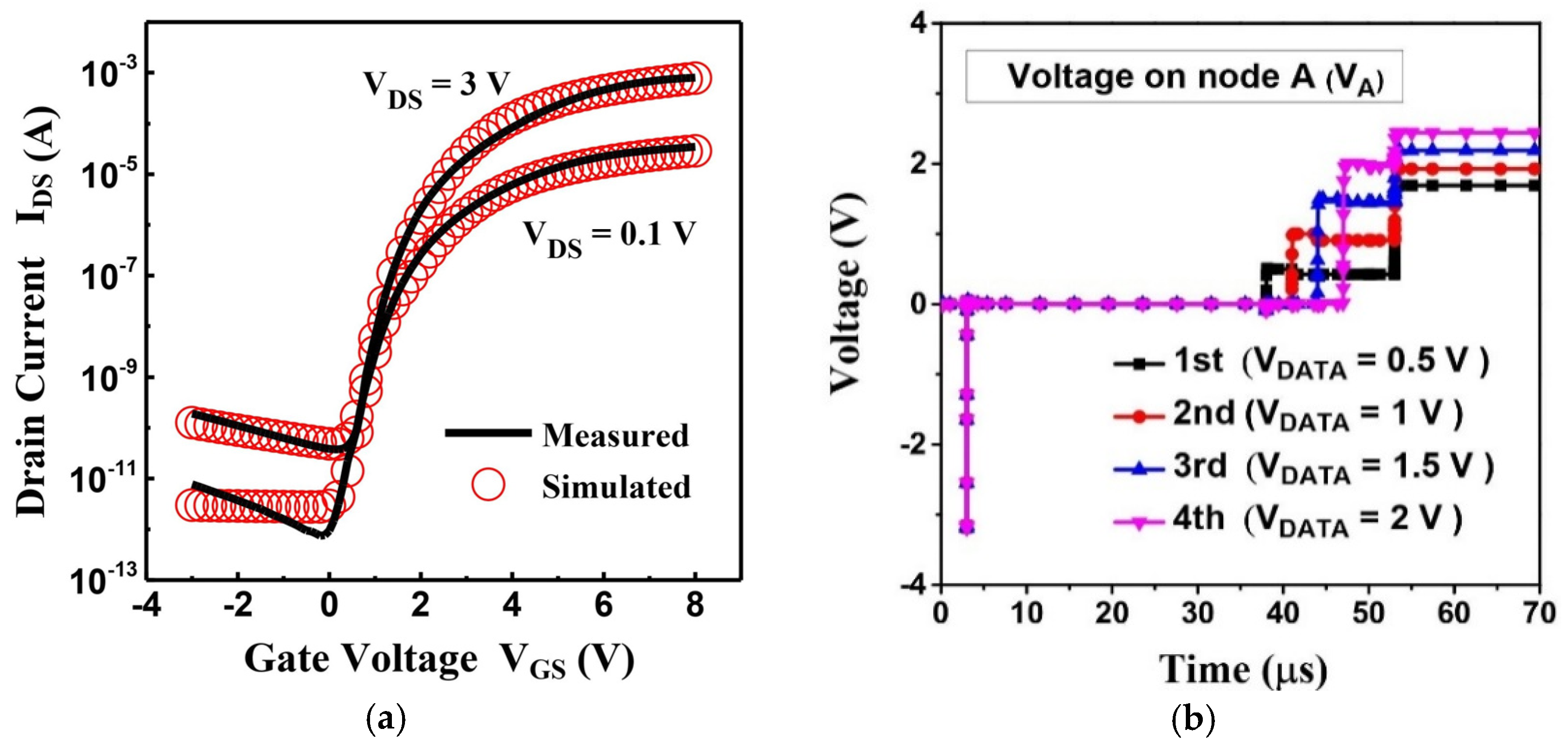
2. TFT Fabrication and Characterization

Figure 1a shows the cross section of the BG-TC n-channel a-IZTO TFTs that were fabricated on glass substrate according to the following procedures. At first, a 250 nm thick ITO was deposited by radio frequency (RF) magnetron sputtering with the power of 30 watt at the base pressure of 5 × 10⁻⁶ torr and the sheet resistivity of the ITO is 7~10 ohm/square and then ITO film was patterned by photolithography and wet etching to form the gate electrode. Then a 180-nm-thick hafnium dioxide (HfO2) was used as the dielectric layer by RF magnetron sputtering in the mixed gas oxygen/argon (O2/Ar) = 40% at room temperature. To enhance the quality of dielectric layer and the bulk defects can be obviously decreased, a post deposition annealing at 250 °C for 1 h by the vacuum oven after the dielectric layer deposition. The contact holes were patterned by photolithography. Then a 90-nm-thick a-IZTO was prepared as channel layer by RF magnetron sputtering process using a target with the atomic ratio of In:Zn:Sn = 1:2:2 at room temperature and patterned by wet etching. Afterward, the source and drain electrodes of the 160-nm-thick titanium (Ti) metal was deposited and patterned by thermal evaporation. Finally, the device was annealed by the vacuum oven at 250 °C for 1 h. In this process, the dimension length [width (W)/length (L)] of all devices are 50/5 μm. The transfer characteristics of the fabricated devices were measured by using an HP4145B semiconductor parameter analyzer and were shown in Figure 1b. Various device parameters, including the threshold voltage (VTH), the subthreshold swing (S.S.), the maximum on-current (ION), and the minimum off-current (IOFF) were measured at a drain voltage of VDS = 3 respectively. The field-effect mobility (μFE) is calculated from the maximum value of the transconductance at VDS = 0.1 V. The fabricated a-IZTO TFT device exhibits a μFE of 70 cm2V−1S−1, S.S. of 0.18 V/decade, ION//IOFF of 5.32 × 10⁷ and VTH of 1.5 V.

3. Proposed Pixel Circuit Operation
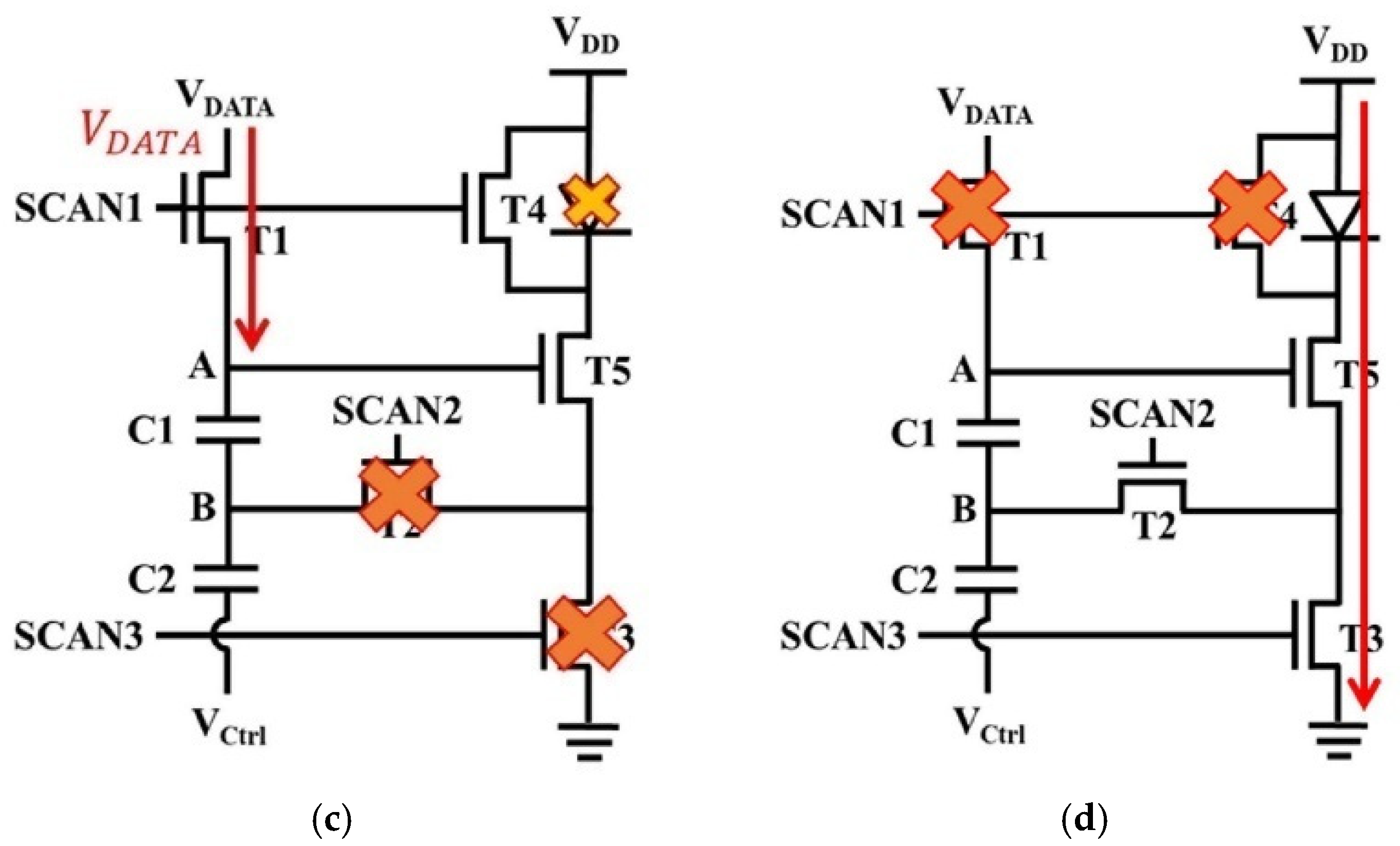
Figure 2a shows the proposed pixel circuit, which comprises four switching TFTs (T1–T4), one driving TFT (T5), and two storage capacitors (C1 and C2). The dimension length [width (W)/length (L)] of the driving TFT is set to 3 μm/10 μm, and those of all switching TFTs are set to 3 μm/3 μm. The capacitances of C1 and C2 are both 0.3 pF. The voltage range of SCAN1, SCAN2, and SCAN3 are from −2 to 5 V. VCtrl is set from −3 to 4 V. VDD and VSS are set to 4.5 and 0 V, respectively. The VTH of the OLED is 1.2 V, and the capacitance in the equivalent circuit of the OLED (COLED) is 0.3 pF. Figure 2b displays the timing diagram of the control signals. The operating period is divided into four periods: reset, compensation, data input, and emission. The operation of the proposed pixel circuit is demonstrated in detail, as shown in Figure 3.

3.1. Reset

In the reset period, all TFTs are turned on by high voltage of all scan lines. The reference voltage, VREF (0 V), is provided to Node A by data line. Node B is reset to VSS (0 V). Thus, the driving TFT is turned off with the gate-to-source voltages of T5 (VGS_TFT) at 0 V.

3.2. Compensation

During the compensation period, T3 is turned off by low voltage of SCAN3, and T1, T2 and T5 are turned on by high voltage of SCAN1 and SCAN2. Because VCtrl switches from VH to VL, the voltage of Node B (VB) is reduced to below zero to make it start charging by T5 until T5 is turned off, and VB turns into −VTH_TFT. Thus, the storage voltage of C 1 is the voltage between VA and VB, which is given by
V C 1 = V A V B = V TH _ T 5

3.3. Data Input

In the data input period, T2 is turn off by the low voltage of SCAN2. The data voltage (VDATA) is given to Node A through T1. With effect of coupling capacitors, VB is varied as shown in the following equation:
V B = V TH _ T 5 + V DATA × C 1 C 1 + C 2
As the result, the storage voltage of C 1 is given by
V C 1 = V TH _ T 5 + V DATA × C 2 C 1 + C 2
Notably, T4 is continuously on during this period to avoid flowing current passing the OLED.

3.4. Emission

During the emission period, T1 and T5 are turned off by low voltage of SCAN1. T2 and T3 are turned on by high voltage of SCAN2 and SCAN3. The OLED current (IOLED) can be expressed as the follows [21]:
I OLED = 1 2 k ( V GS V TH _ T 5 ) 2 = 1 2 k ( V TH _ T 5 + V DATA × C 2 C 1 + C 2 V TH _ T 5 ) 2 = 1 2 k ( V DATA × C 2 C 1 + C 2 ) 2
where k is μ × COX × W/L. By (4), the OLED current is not dependent of the VTH of T5/OLED voltage/voltage of power line (VDD). Thus, the drop in VDD, OLED degradation, and VTH shift of the driving TFT are compensated simultaneously. Besides, the use of high-mobility a-IZTO TFTs in pixel circuit can supply high driving current at low driving voltage. This implies that the same output current of driving TFT can be provided with lower driving voltage. It believes that the circuit can compensate well against VTH shifts of driving TFT, OLED degradation and I-R drop and be driven in low voltage at the same time.

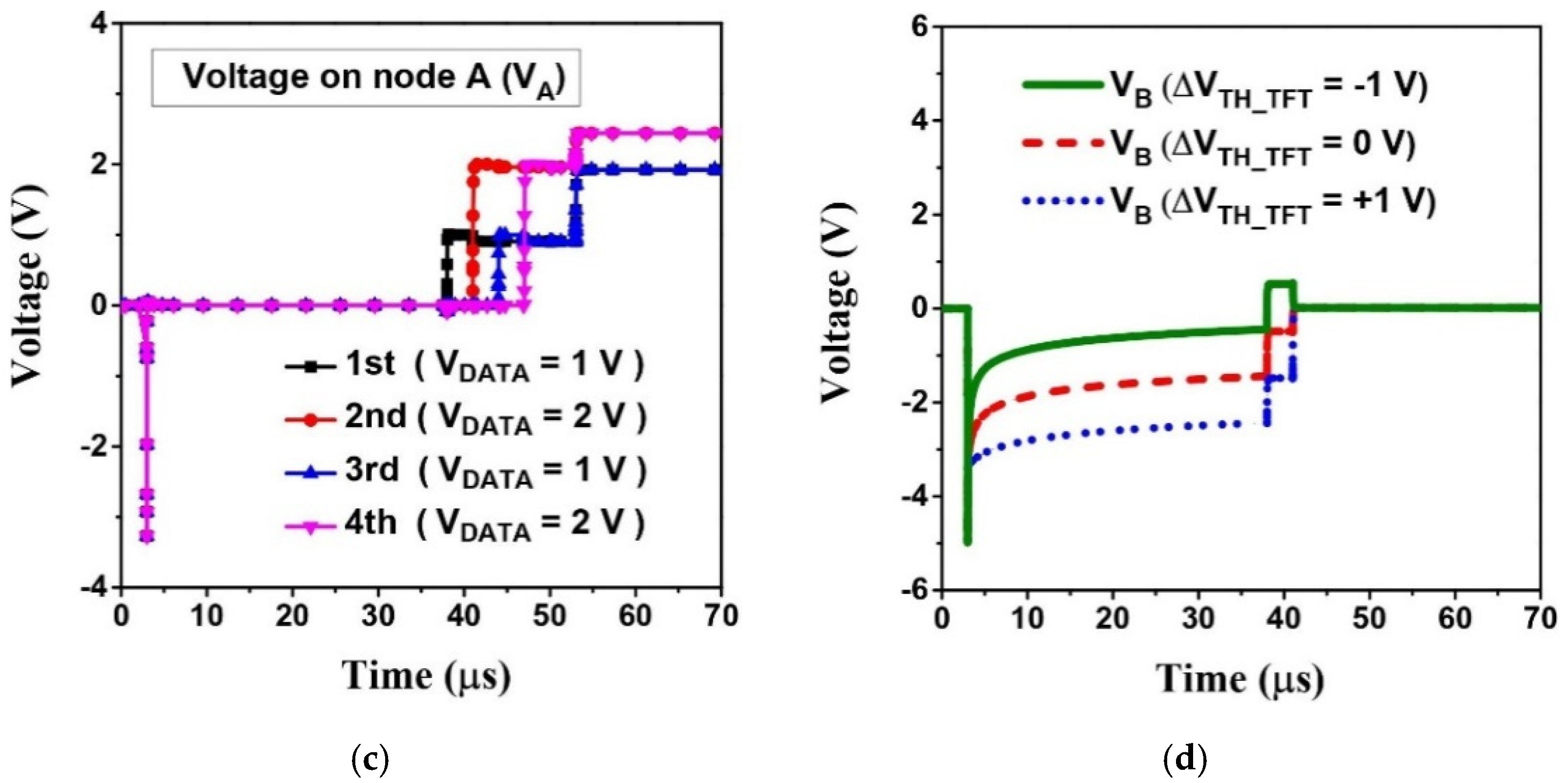
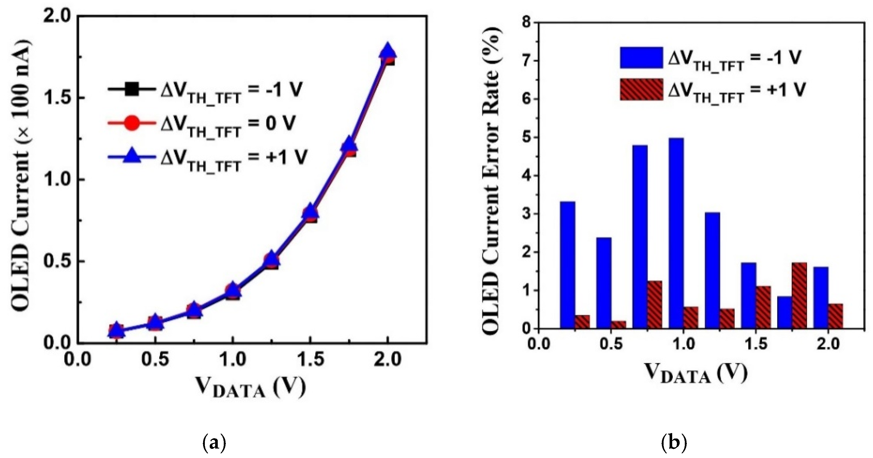
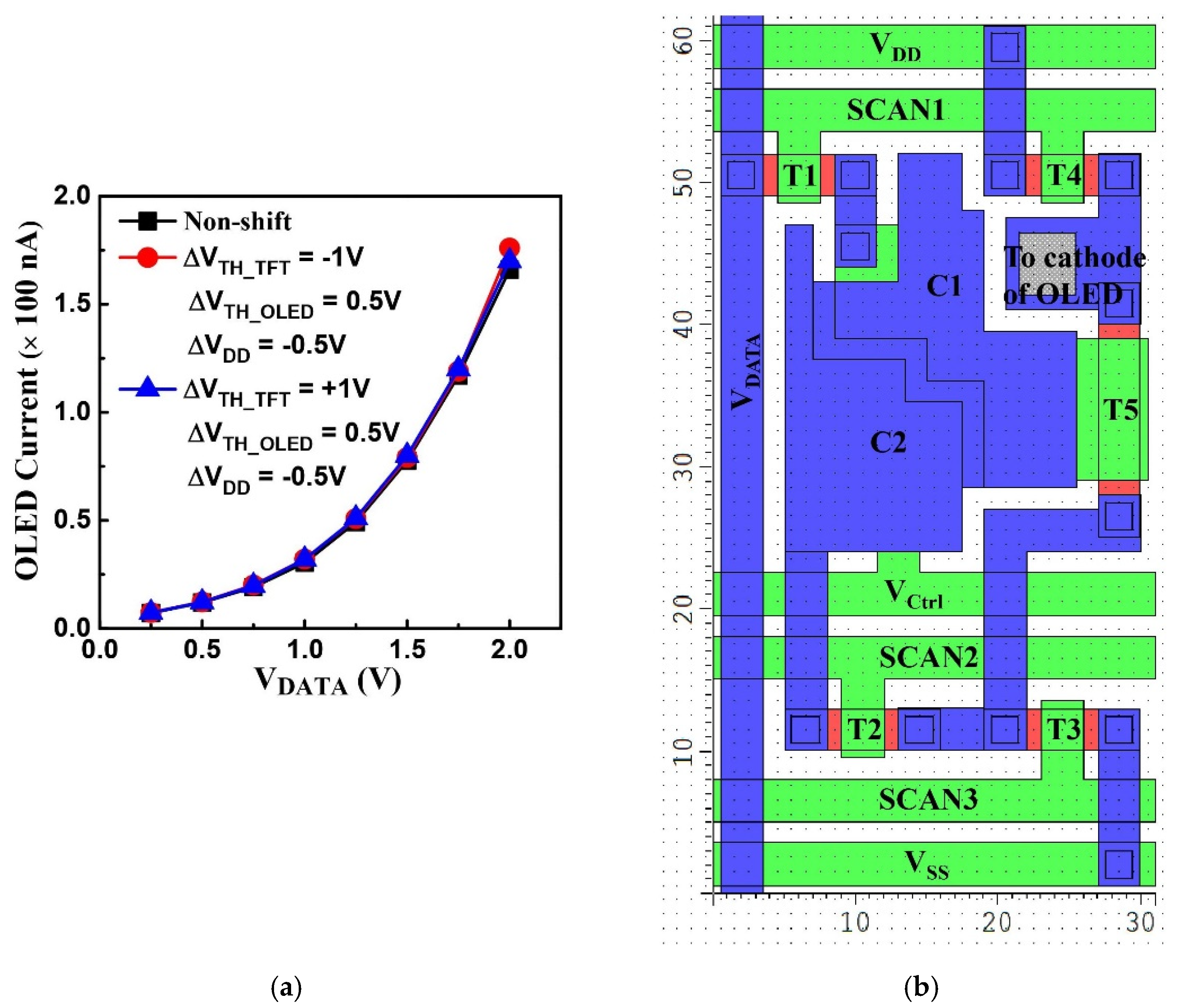
4. Results and Discussion

To verify its feasibility, the proposed circuit was simulated using AIM-SPICE and the transfer curve of the TFT were measured and fitted, as presented in Figure 4a. The mobility and VTH of the device were 70 cm2V−1S−1 and 1.5 V, respectively. Herein, the time taken to input data in each row was set to 3 μs when used for Full-HD+ (2400 × 1080) at the frame rate 120 Hz. Figure 4b plots the simulated transient waveforms of Node A (VA) of the pixels from 1st to 4th rows with different data voltage (VDATA = 0.5, 1, 1.5 and 2 V) to ensure that the VA receive the signals correctly. Figure 4c shows the simulated transient waveforms of VA with the same data voltage (VDATA = 1 V) is put into the pixels for the 1st and 3rd row, a different VDATA of 2 V is put into the pixels for the 2nd and 4th rows in data input period. As a result, the data voltage of the 1st row is equal to the 3rd row one and the same result is also gotten for the pixels of the 2nd and 4th row. Thus, Figure 4b,c show this proposed pixel circuit operates correctly in each row. Figure 4d shows the simulated transient waveforms of Node B for this proposed 5T2C pixel circuit when the voltage of the driving TFT (VTH_TFT) was varied by ±1 V. As displayed in Figure 4d, the shifted VTH_TFT was sensed and stored by this proposed pixel circuit successfully.
Figure 5a plots OLED currents with different VDATA when VTH of driving TFT was shifted by ±1 V. Figure 5b shows the current error rates at different gray levels with ΔVTH_TFT = ±1 V. All error rates were lower than 4.97% under different VDATA, which indicated high immunity against VTH variation of the driving TFT.
Moreover, the VTH of OLED increases when it is operated for a long period [22]. To verify the ability of this proposed circuit to compensate for OLED degradation (VTH_OLED), the VTH of the OLED was degraded from 0 to 0.5 V. As illustrated in Figure 6a, when the VTH of OLED was increased at high, middle, and low gray levels, the maximum OLED current variation of this proposed pixel circuit was significantly low as 0.1%, 0.18%, and 0.16%, respectively. Therefore, we confirmed that the proposed pixel circuit effectively compensates for OLED degradation. Figure 6b shows the OLED current versus the VDD drop. Different VDATA were given to observe this influence when VDD dropped at different voltages. The maximum current errors at the high, middle, and low gray level were 0.09%, 0.11%, and 0.19% respectively, which revealed the effective suppression of current fluctuation. Figure 7a presents the driving currents versus input data voltages of ΔVTH_TFT = ±1 V, ΔVDD = 0.5 V, and ΔVTH_OLED = 0.5 V. The maximum current error rate was 5.71%. Therefore, the 5T2C pixel circuit was confirmed to simultaneously compensate for VTH variation in the driving TFT, OLED degradation, and I-R drops of VDD. Figure 7b shows the layout of a sub-pixel of this proposed pixel circuit. It satisfied the requirement of 6.6-inch Full-HD + (2400 × 1080) displays with layout area of 32 μm × 64 μm.
The results are presented and compared with the reported AMOLED pixel circuits in Table 1, where circle and cross show the circuits with and without the compensation ability, respectively. Y. Kim et al. [17] presented a 5T1C pixel circuit with the enhanced reliability, but it can’t compensate the OLED degradation. Although other reported circuits [18,19,20] could compensate VTH variation of the TFT, OLED degradation, and I-R drop of VDD, only the proposed pixel circuit could operate with low driving voltage (<5 V). The proposed pixel circuit using a-IZTO TFT as a driving device is thus a favorable candidate to simultaneously compensate for VTH, I-R drop, and OLED degradation problems in portable displays with high resolution.

5. Conclusions

A low-voltage driving pixel circuit (<5 V) with high-mobility a-IZTO TFT was proposed for use in AMOLED displays for high-resolution portable applications. The non-uniformity in the display image generated by VTH shifts in the driving TFT, I-R drops of the power line, and OLED degradation could all be compensated with this proposed pixel circuit. The compensated OLED current error rates were lower than 5.71% for all input data when ΔVTH_TFT of ±1 V, ΔVDD of 0.5 V, and ΔVTH_OLED of 0.5 V were all considered. Accordingly, we expect the circuit to be highly suitable for high-resolution portable applications with high-mobility a-IZTO TFTs as driving devices.

Author Contributions

Conceptualization, C.-L.F. and C.-Y.C.; Formal analysis, P.-C.C.; Methodology, H.-Y.T.; Software, P.-C.C.; Writing—original draft, P.-C.C. and W.-Y.L.; Writing—review & editing, C.-L.F., H.-Y.T., C.-Y.C. and W.-Y.L. All authors have read and agreed to the published version of the manuscript.

Funding

This research received no external funding.

Acknowledgments

The authors would like to acknowledge the equipment support from National Nano Device Laboratories (NDL), and the simulator software support from Taiwan Semiconductor Research Institute (TSRI).

Conflicts of Interest

The authors declare no conflict of interest.

References

  1. Dawson, R.M.A.; Shen, Z.; Furst, D.A.; Connor, S.; Hsu, J.; Kane, M.G.; Stewart, R.G.; Ipri, A.; King, C.N.; Green, P.J.; et al. The impact of the transient response of organic light emitting diodes on the design of active matrix OLED displays. In Proceedings of the International Electron Devices Meeting 1998, Technical Digest (Cat. No.98CH36217), San Francisco, CA, USA, 6–9 December 1998; pp. 875–878. [Google Scholar]
  2. Wang, C.; Hu, Z.; He, X.; Liao, C.; Zhang, S. One gate diode-connected dual-gate a-IGZO TFT driven pixel circuit for active matrix organic light-emitting diode displays. IEEE Trans. Electron Devices 2016, 63, 3800–3803. [Google Scholar] [CrossRef]
  3. Fan, C.L.; Chen, Y.C.; Yang, C.C.; Tsai, Y.K.; Hung, B.R. Novel LTPS-TFT pixel circuit with OLED luminance compensation for 3D AMOLED displays. J. Disp. Technol. 2016, 12, 425–428. [Google Scholar] [CrossRef]
  4. Lin, C.L.; Chen, Y.C. A novel LTPS-TFT pixel circuit compensating for TFT threshold-voltage shift and OLED degradation for AMOLED. IEEE Electron Device Lett. 2007, 28, 129–131. [Google Scholar] [CrossRef]
  5. Lu, H.Y.; Chang, T.C.; Tai, Y.H.; Liu, P.T.; Chi, S. A new pixel circuit compensating for brightness variation in large size and high resolution AMOLED displays. J. Disp. Technol. 2007, 3, 398–403. [Google Scholar]
  6. Lin, C.L.; Chang, J.H.; Lai, P.C.; Shih, L.W.; Chen, S.C.; Cheng, M.H. Pixel circuit with leakage prevention scheme for low-frame-rate AMOLED displays. IEEE J. Electron Devices Soc. 2020, 8, 235–240. [Google Scholar] [CrossRef]
  7. Nathan, A.; Chaji, G.R.; Ashtiani, S.J. Driving schemes for a-Si and LTPS AMOLED displays. J. Disp. Technol. 2005, 1, 267–277. [Google Scholar] [CrossRef]
  8. Ma, P.; Sun, J.; Zhang, G.; Liang, G.; Xin, Q.; Li, Y.; Song, A. Low–temperature fabrication of HfAlO alloy dielectric using atomic–layer deposition and its application in a low–power device. J. Alloys Compd. 2019, 792, 543–549. [Google Scholar] [CrossRef]
  9. Lin, C.L.; Chen, F.H.; Hung, C.C.; Chen, P.S.; Deng, M.Y.; Lu, C.M.; Huang, T.H. New a-IGZO pixel circuit composed of three transistors and one capacitor for use in high-speed-scan AMOLED displays. J. Disp. Technol. 2015, 11, 1031–1034. [Google Scholar]
  10. Xu, H.; Li, M.; Wang, L.; Xu, M.; Ning, H.; Peng, J. Flexible AMOLED based on oxide TFT with high mobility. SID Symp. Dig. Tech. Pap. 2017, 48, 342–344. [Google Scholar]
  11. Fuh, C.S.; Liu, P.T.; Huang, W.H.; Sze, S.M. Effect of annealing on defect elimination for high mobility amorphous indium-zinc-tin-oxide thin-film transistor. IEEE Electron Device Lett. 2014, 35, 1103–1105. [Google Scholar] [CrossRef]
  12. Song, J.H.; Kim, K.S.; Mo, Y.G.; Choi, R.; Jeong, J.K. Achieving high field-effect mobility exceeding 50 cm2/Vs in In-Zn-Sn-O thin-film transistors. IEEE Electron Device Lett. 2014, 35, 853–855. [Google Scholar] [CrossRef]
  13. Mude, N.N.; Bukke, R.N.; Saha, J.K.; Avis, C.; Jang, J. Highly stable, solution-processed Ga-doped IZTO thin film transistor by Ar/O2 plasma treatment. Adv. Electron. Mater. 2019, 5, 1900768. [Google Scholar] [CrossRef]
  14. Lestari, A.D.; Noviyana, I.; Putri, M.; Heo, Y.W.; Lee, H.Y. Effect of the active channel thickness variation in amorphous In–Zn–Sn–O thin film transistor. Nanotechnology 2019, 19, 1686–1689. [Google Scholar] [CrossRef] [PubMed]
  15. Li, R.; Dai, S.; Su, J.; Ma, Y.; Wang, Y.; Zhou, D.; Zhang, X. Effect of thermal annealing on the electrical characteristics of an amorphous ITZO:Li thin film transistor fabricated using the magnetron sputtering method. Mater. Sci. Semicond. Process. 2019, 96, 8–11. [Google Scholar] [CrossRef]
  16. Ono, S.; Miwa, K.; Maekawa, Y.; Tsujimura, T. VT compensation circuit for AM OLED displays composed of two TFTs and one capacitor. IEEE Trans. Electron Devices 2007, 54, 462–467. [Google Scholar] [CrossRef]
  17. Kim, Y.; Kim, Y.; Lee, H. A novel a-InGaZnO TFT pixel circuit for AMOLED display with the enhanced reliability and aperture ratio. J. Disp. Technol. 2014, 10, 80–83. [Google Scholar] [CrossRef]
  18. Kim, D.; Kim, Y.; Lee, S.; Kang, M.S.; Kim, D.H.; Lee, H. High resolution a-IGZO TFT pixel circuit for compensating threshold voltage shifts and OLED degradations. IEEE J. Electron Devices Soc. 2017, 5, 372–377. [Google Scholar] [CrossRef]
  19. Lin, C.L.; Liu, Y.T.; Lee, C.E.; Chen, P.S.; Chu, T.C.; Hung, C.C. a-InGaZnO active-matrix organic LED pixel periodically detecting thin-film transistor threshold voltage once for multiple frames. IEEE Electron Device Lett. 2015, 36, 1166–1168. [Google Scholar] [CrossRef]
  20. Lai, P.C.; Lin, C.L.; Kanicki, J. Novel top-anode OLED/a-IGZO TFTs pixel circuit for 8K4K AM-OLEDs. IEEE Trans. Electron Devices 2019, 66, 436–444. [Google Scholar] [CrossRef]
  21. Sze, S.M. Physics of Semiconductor Devices; Wiley: New York, NY, USA; National Taiwan University Press: Taibei, Taiwan, 2018; pp. 186–192. [Google Scholar]
  22. In, H.J.; Kwon, O.K. External compensation of nonuniform electrical characteristics of thin-film transistors and degradation of OLED devices in AMOLED displays. IEEE Electron Device Lett. 2009, 30, 377–379. [Google Scholar]
Figure 1. (a) Schematic cross-sectional diagram and (b) measured transfer characteristics of the a-IZTO TFT.
Coatings 10 01004 g001
Figure 2. Proposed pixel circuit. (a) Circuit schematic. (b) Timing diagram.
Coatings 10 01004 g002
Figure 3. Schematic of circuit operation in various periods with (a) reset (b) compensation (c) data input (d) emission period.
Coatings 10 01004 g003aCoatings 10 01004 g003b
Figure 4. (a) Measured and simulated transfer curves of the a-IZTO TFT. (b) Transient waveforms of VA with first to fourth rows in different VDATA. (c) Transient waveforms of VA with VDATA = 1 V for Row1 and Row3, VDATA = 3 V for Row2 and Row4. (d) Transient waveforms of VB of the proposed pixel circuit with ±1 V variation in VTH_TFT.
Coatings 10 01004 g004aCoatings 10 01004 g004b
Figure 5. (a) Driving currents versus data voltage with ±1 V variation in VTH_TFT. (b) OLED current error rates with ±1 V variation in VTH_TFT.
Coatings 10 01004 g005
Figure 6. (a) OLED currents of different VDATA when VTH_OLED shifts from 0 to 0.5 V. (b) OLED currents of different data voltages when VDD drops by 0.5 V.
Coatings 10 01004 g006
Figure 7. (a) OLED current versus data voltage with VTH shift of the driving TFT, VTH_OLED shift of OLED degradation, and I-R drop of VDD. (b) Layout of the proposed 5T2C pixel circuit.
Coatings 10 01004 g007
Table 1. Comparison of proposed and prior pixel circuits.
ReferenceDriving Voltage (VDD & VSS)VTH_DTFT Variation Error RateOLED CompensationEliminate in I-R Drop of VDD
This studyVDD = 4.5 V
VSS = 0 V
4.97% (ΔVTH = ±1 V)OO
[17]VDD = 15 V
VSS = 0 V
7% (ΔVTH = ±2 V)XO
[18]VDD = 15 ~ −5 V
VSS = 0 V
9.4% (ΔVTH = ±2 V)OO
[19]VDD = 9.75 V
VSS = −7 V
4.14% (ΔVTH = +1 V)OO
[20]VDD = 13 V
VSS = −7 V
4.42% (ΔVTH = ±2 V)OO
Publisher’s Note: MDPI stays neutral with regard to jurisdictional claims in published maps and institutional affiliations.

