Review

A Review of Readout Circuit Schemes Using Silicon Nanowire Ion-Sensitive Field-Effect Transistors for pH-Sensing Applications

1
Department of Intelligent Semiconductor and Display Engineering, Kookmin University, Seoul 02707, Republic of Korea
2
School of Electrical Engineering, Kookmin University, Seoul 02707, Republic of Korea
3
Department of Artificial Intelligence Semiconductor Engineering, Hanyang University, Seoul 04763, Republic of Korea
4
Department of Electronic Engineering, Hanyang University, Seoul 04763, Republic of Korea
*
Authors to whom correspondence should be addressed.
These authors contributed equally to this work.
Biosensors 2025, 15(4), 206; https://doi.org/10.3390/bios15040206
Submission received: 19 January 2025 / Revised: 7 March 2025 / Accepted: 20 March 2025 / Published: 22 March 2025
(This article belongs to the Special Issue Biosensors Based on Transistors)

Abstract

:
This paper reviews various design approaches for sensing schemes that utilize silicon nanowire (SiNW) ion-sensitive field-effect transistors (ISFETs) for pH-sensing applications. SiNW ISFETs offer advantageous characteristics, including a high surface-to-volume ratio, fast response time, and suitability for integration with complementary metal oxide semiconductor (CMOS) technology. This review focuses on SiNW ISFET-based biosensors in three key aspects: (1) major fabrication processes and device structures; (2) theoretical analysis of key performance parameters in readout circuits such as sensitivity, linearity, noise immunity, and output range in different system configurations; and (3) an overview of existing readout circuits with quantitative evaluations of N-type and P-type current-mirror-based circuits, highlighting their strengths and limitations. Finally, this paper proposes a modified N-type readout scheme integrating an operational amplifier with a negative feedback network to overcome the low sensitivity of conventional N-type circuits. This design enhances gain control, linearity, and noise immunity while maintaining stability. These advancements are expected to contribute to the advancement of the current state-of-the-art SiNW ISFET-based readout circuits.

1. Introduction

In modern drug development and disease treatment, early diagnosis and testing are critical as they assess a patient’s current status and provide key information for the next stages. Typically, early diagnosis has been conducted through various biomolecule-sensing methods, including electrochemical detection [1,2], optical detection [3,4], and mass spectrometry [5,6]. Electrochemical detection measures electrical changes resulting from chemical reactions between target biomolecules and functionalized elements (primarily enzymes), using their specific binding and catalytic properties to detect and quantify biomolecules [7]. Optical detection uses the ability of target molecules to absorb or emit light. Mass spectrometry is employed for the detection of target molecules, directly measuring their mass. However, these conventional methods are often limited by lengthy detection times, high costs, complex equipment, and the need for skilled operators and specialized laboratory environments, constraining their practicality in terms of accessibility, maintenance, and scalability.
In this regard, semiconductor-based biosensor technologies have received significant attention these days [8,9,10,11]. Semiconductor biochips have several advantages, such as the ability to perform point-of-care diagnostics without spatial or temporal constraints. In addition, these biochips can be miniaturized, making them more practical and cost-efficient for large-scale manufacturing environments [9,12,13]. Moreover, these technologies leverage the electrical properties of semiconductor devices to detect biological changes, enabling applications in diverse fields such as medical diagnostics and chemical analysis [14,15]. For example, field-effect transistor (FET)-based biosensors utilizing complementary metal oxide semiconductor (CMOS) technology have been used due to their high sensitivity and rapid response in detecting SARS-CoV-2 spike proteins, enabling effective pandemic-related diagnostics [16].
The development of semiconductor biochips involves the utilization of various types of transistors, with CMOS technology being one of the most widely used platforms. CMOS-based biochips integrate transistors and physical sensing materials on a single chip, reducing costs while enabling multi-functionality in a compact form factor. In general, CMOS biosensors offer advantages such as low power consumption, multi-modality sensing, short response time, and label-free detection [17,18,19,20,21,22,23,24,25,26]. In the literature, graphene field-effect transistor (GFET) technology leverages the unique properties of the two-dimensional carbon material graphene [27,28,29,30,31,32,33]. GFETs enable fast sensing capabilities due to their high electrical conductivity, and they enhance a signal-to-noise ratio (SNR) due to low electrical noise characteristics [34]. Next, ion-sensitive FETs (ISFETs), first proposed by Bergveld in 1970 [35], have been widely used for biomolecule detection. Unlike traditional three-electrode setups, ISFETs require only a single reference electrode, simplifying instrumentation. In addition, as robust solid-state sensors, ISFETs demonstrate high resistance to acidic and alkaline environments as well as physical damage [36,37].
Among various semiconductor technologies, nanoscale ISFETs in the form of a silicon nanowire (SiNW) have attracted significant attention for overcoming the physical limitations inherent in sensors fabricated with planar semiconductor technologies [38,39,40,41,42]. Their nanoscale structure enhances sensitivity, allowing for the detection of ultralow concentrations of biomolecules [43,44], while their reduced footprint makes them well-suited for high-density sensor arrays [42,45]. Additionally, SiNW ISFETs offer several advantages such as a high surface-to-volume ratio [46], real-time monitoring [8], and label-free detection capabilities like CMOS sensors [8,43,47,48,49]. These properties have been applied in detecting pH concentrations [50,51,52,53], nucleic acids [48,54,55,56,57,58,59,60], proteins [47,61,62,63,64,65,66,67,68], cells [69,70,71], protein–DNA interactions [20,25,72,73,74,75], and single-virus detection [76]. In addition, SiNW ISFETs are increasingly being integrated with artificial intelligence (AI), machine learning (ML), and internet-of-things (IoT) frameworks to enhance biosensor capabilities [77,78]. ML-optimized models have demonstrated higher precision and reliability than conventional physics-based models while maintaining robustness against environmental variations and noise, making them well-suited for real-time biosensor applications [79]. Moreover, SiNW ISFETs offer key advantages, including high reproducibility and compatibility with standard CMOS technology. These benefits have been demonstrated in biomolecular diagnostic systems by integrating top-down-fabricated SiNW ISFETs with CMOS circuits [80,81].
In the field of pH sensing, ISFET-based techniques fundamentally involve the changes in threshold voltage (VTH) due to ion concentration [82]. To enhance ISFET performance, many studies have focused on improving sensitivity, reducing noise, and mitigating environmental effects. To increase sensitivity, methods such as the extended gate have been proposed [83]. For noise suppression, studies have investigated aptamer-based functionalization, which selectively captures target molecules and prevents the adhesion of interfering substances, thereby enhancing the SNR [84,85]. In addition, differential ISFET configurations [86] and signal conditioning techniques [87] have been proposed to achieve temperature compensation. Research has also focused on electrode modifications using gold nanoparticles (AuNPs) to enhance potential signal strength [88,89]. A surface modification with aromatic diazonium salt membranes has been examined to precisely control the anchoring layer thickness, aligning it with the Debye length for optimized sensor performance [90,91]. These advancements contribute to enhancing biosensor accuracy and reliability.
The design of readout systems requires careful optimization of critical performance parameters, including dynamic range (DR), resolution, output range, sensitivity (gain), and linearity (Figure 1). In general, a wider DR is advantageous because DR represents the concentration range of target biomolecules (Cmole) that can be sensed by readout circuits. The resolution refers to the smallest change in the input that can be reliably detected by the readout system regardless of DR; a higher resolution indicates an ability to distinguish finer variations [12]. The output range determines the maximum and minimum limits of the output signal that the circuit can generate, which directly affects DR. If the output range is too narrow, the DR may be limited, resulting in distortions or loss of information. A higher gain is typically preferred, but it potentially degrades linearity, indicating complex trade-offs that need to be considered. In readout circuit design, it is essential to manage the balance among these parameters. Figure 2 and Figure 3 illustrate the relationship between key properties of the system. It is shown that a voltage headroom affects the available output and DR (Figure 2), whereas a high sensitivity lowers a DR (Figure 3).
The existing review articles [92,93,94,95] have mainly focused on the general applications of ISFET sensors, particularly the detection of biomolecules such as DNA, proteins, and antibodies, and their commercialization potential. However, these reviews lack a critical analysis of recent circuit design technologies specific to SiNW ISFETs and their impact on sensor performance. For example, Cao et al. [92] discuss the applications of ISFET sensors in biomolecule detection and their commercialization prospects but provide little discussion of circuit design and optimization. Similarly, Sinha et al. [93] extensively cover materials, fabrication technologies, and modeling methods of FET-based pH sensors, yet offer limited discussion on recent advancements in circuit design and their impact on performance. Baghini et al. [94] focus on ultra-thin ISFET sensing systems, discussing noise compensation circuits, flexible electronics, and readout circuit design, but lack specific coverage of the SiNW ISFET technology and a quantitative comparison of circuit-level optimization. In contrast, Moser et al. [95] explore recent trends in CMOS ISFET instrumentation, focusing on advancement in front-end circuit topologies for ISFET arrays and addressing key challenges such as offset and drift compensation. Nevertheless, their review does not include a detailed comparison of SiNW ISFET technology or recent improvements in readout circuit architectures tailored for this technology.
To address the limitations of previous reviews, this paper provides a targeted and in-depth analysis of SiNW ISFET readout circuits, particularly examining how circuit design choices impact key performance parameters such as sensitivity, noise immunity, linearity, and output range. Unlike prior works that primarily emphasize material properties and device fabrication, this study presents a quantitative and comparative evaluation of various readout circuit topologies, including conventional SiNW-based biosensors [8], sensitivity-enhanced structures [96], and SiNW/CMOS hybrid circuits [97]. The differences between this paper and previous reviews are summarized in Table 1. A detailed circuit-level analysis is conducted, focusing on current mirror-based circuits using P-type and N-type SiNW ISFETs [12,98], highlighting the trade-offs and performance improvements achieved through various design approaches. Additionally, this paper introduces a modified N-type readout circuit that integrates an operational amplifier (op-amp) with a negative feedback network to overcome the low sensitivity of conventional N-type designs. By optimizing the circuit topology, the proposed design enhances gain control, expands output range, and significantly reduces susceptibility to power supply noise while maintaining stability, making it more suitable for real-time and high-precision biosensor applications.
The organization of this paper is as follows. Section 2 reviews the key fabrication processes and methods of SiNW ISFETs. Section 3 explains the main properties of SiNW ISFETs as hydrogen ion sensors. Section 4 discusses key performance metrics and related theories of SiNW-based readout systems, along with an analysis of existing circuits. Section 5 introduces a modified N-type readout circuit and compares its performance with existing circuits to evaluate its potential. Finally, Section 6 summarizes the findings of this paper. For abbreviated terms used throughout, readers may refer to Table 2.

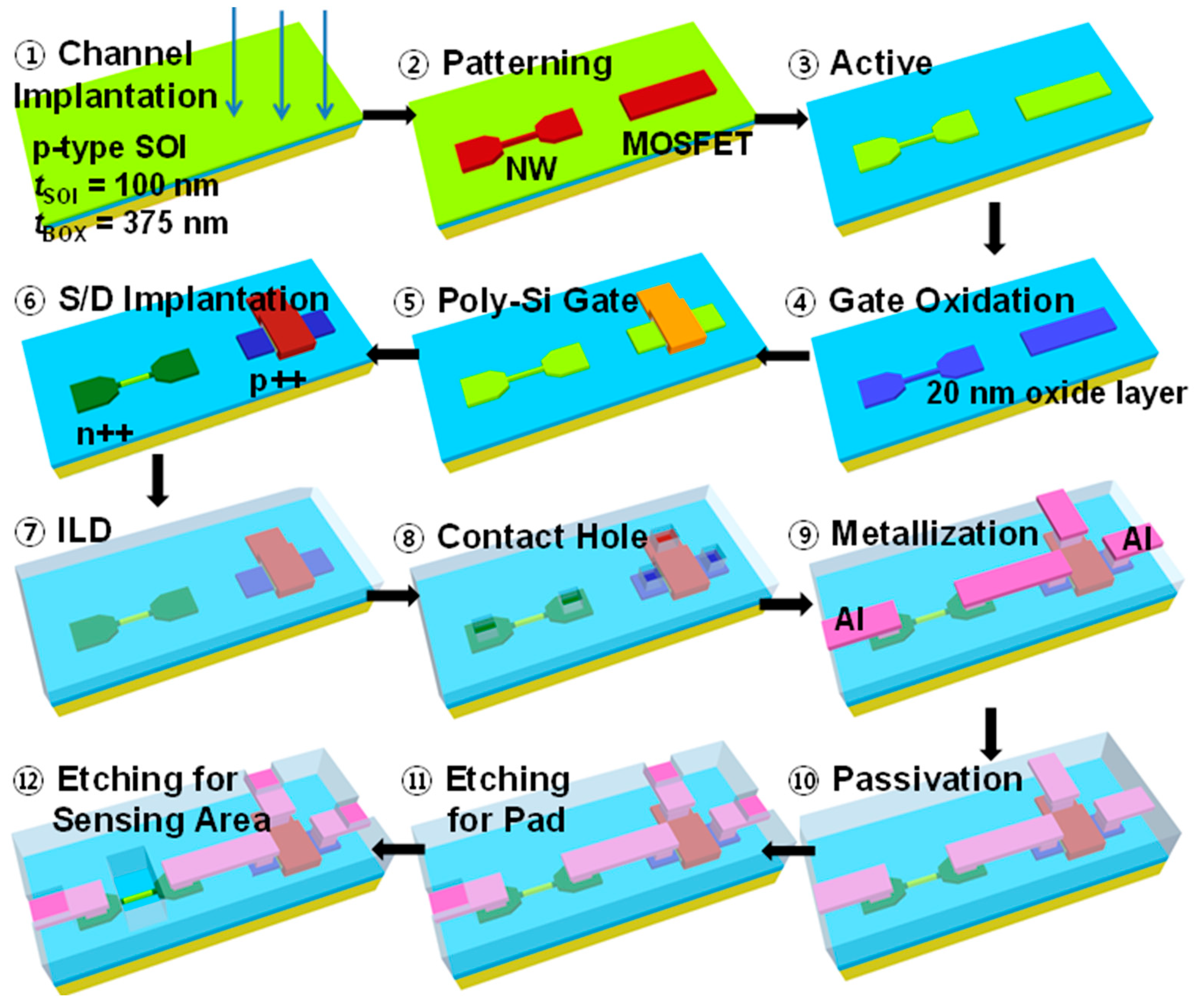
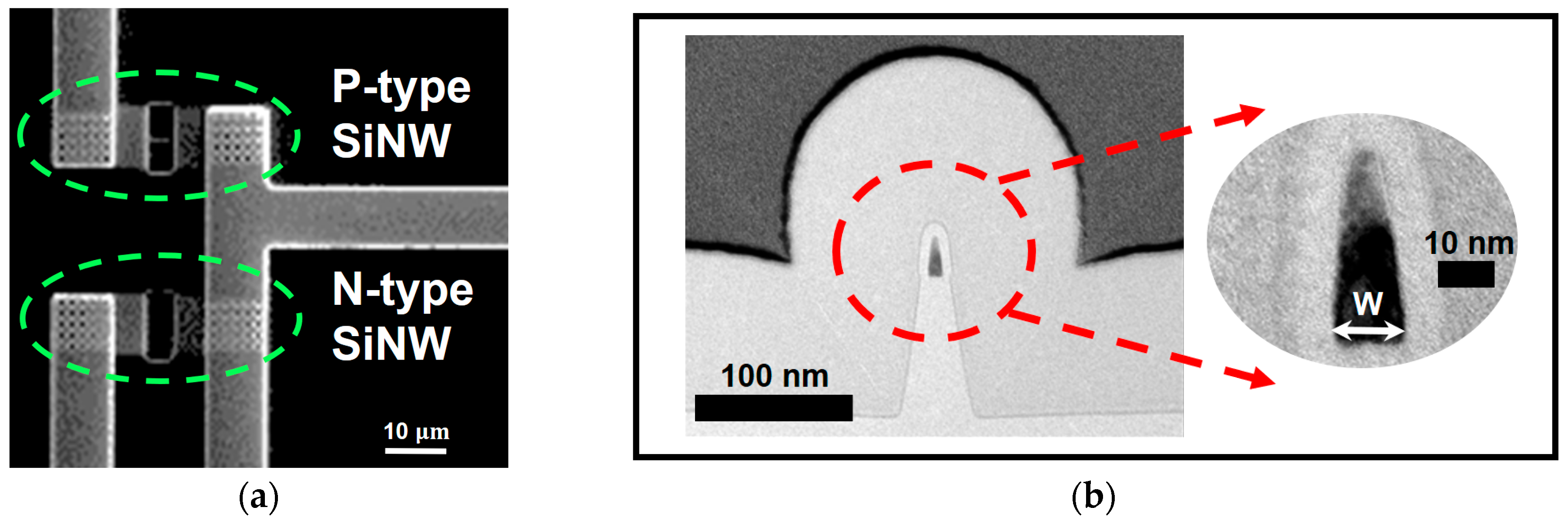
2. Fabrication Process of a SiNW ISFET

As a key component of semiconductor biochips, it is worth reviewing the major process steps in a SiNW ISFET. Various fabrication methods have been proposed and applied to implement a SiNW [8,17,47,63,99,100,101,102,103]. The SiNW ISFET, a pivotal component of semiconductor biochips, can be manufactured through two principal methodologies: the bottom-up and top-down. The bottom-up approach involves the synthesis of SiNWs from molecular precursors [104,105,106], allowing precise control of the dimensions and morphology of the nanowires at the angstrom to nanometer scale, as well as the production of intricate superlattice structures. On the other hand, this method faces significant challenges, including low device uniformity, poor manufacturing yield, and difficulties in CMOS integration, making it currently unsuitable for large-scale biosensor production.
In contrast, the top-down approach utilizes lithography-based techniques to shape SiNWs from bulk silicon wafers. This method is widely used due to its high manufacturing yield, cost-effectiveness, and seamless integration with the CMOS environment [48,61,107,108,109,110,111,112]. Particularly advantageous for large-scale production, this approach enables the fabrication of SiNW biosensors alongside CMOS readout circuits [8,48,100,101,102,103,113,114,115]. Table 3 provides a summarized comparison of the advantages and limitations of the bottom-up and top-down methods, including aspects not fully covered in the text.
The top-down fabrication process of SiNW ISFETs integrated with CMOS devices is illustrated in Figure 4. The biosensors were fabricated on a boron-doped (4 × 1015 cm⁻3) 6-inch (100) silicon-on-insulator (SOI) wafer, with a 100 nm thick top Si layer separated from the Si substrate by a 375 nm thick buried oxide (BOX). The process begins with the growth of a 20 nm thick buffer oxide layer on the silicon surface for protection during channel implantation. Boron and phosphorus ions are implanted into the P-type and N-type regions, respectively, to define the channel structure (Step 1). After annealing, the active regions are patterned using a combination of e-beam lithography and photolithography (Step 2). Anisotropic etching is performed on the silicon layer with hydrogen silsesquioxane (HSQ) and photoresist (PR) masks, followed by inductively coupled plasma (ICP) etching in an HBr/O2 plasma, forming the SiNWs and CMOS regions (Step 3). Subsequently, the gate oxide layer is grown through dry oxidation at 850 °C, resulting in a 20 nm thick dielectric layer (Step 4). Poly-Si gates are deposited using low-pressure chemical vapor deposition (LPCVD) and patterned using photolithography (Step 5).
Then, the source and drain regions are doped with arsenic ions for N-type regions and boron ions for P-type regions via ion implantation, followed by high-temperature annealing for dopant activation (Step 6). A high-density plasma chemical vapor deposition (HDP-CVD) process is employed to deposit an inter-layer dielectric (ILD), which is planarized using chemical mechanical planarization (CMP) (Step 7). Contact holes are formed via photolithography and etching to expose the source, drain, and gate regions (Step 8). Metallization is performed through aluminum sputtering and patterning to create interconnections (Step 9), and a tetraethyl orthosilicate (TEOS) oxide passivation layer is deposited to protect the structures (Step 10). Finally, the sensing area of the SiNW channel is exposed by selectively etching the TEOS layer, enabling interaction with biomolecule analyzes, and the oxide on the metal pads is etched to expose the electrical contacts (Steps 11–12). Figure 5 presents a transmission electron microscopy (TEM) image of a cross-sectional view of the SiNW ISFET channel region [97].

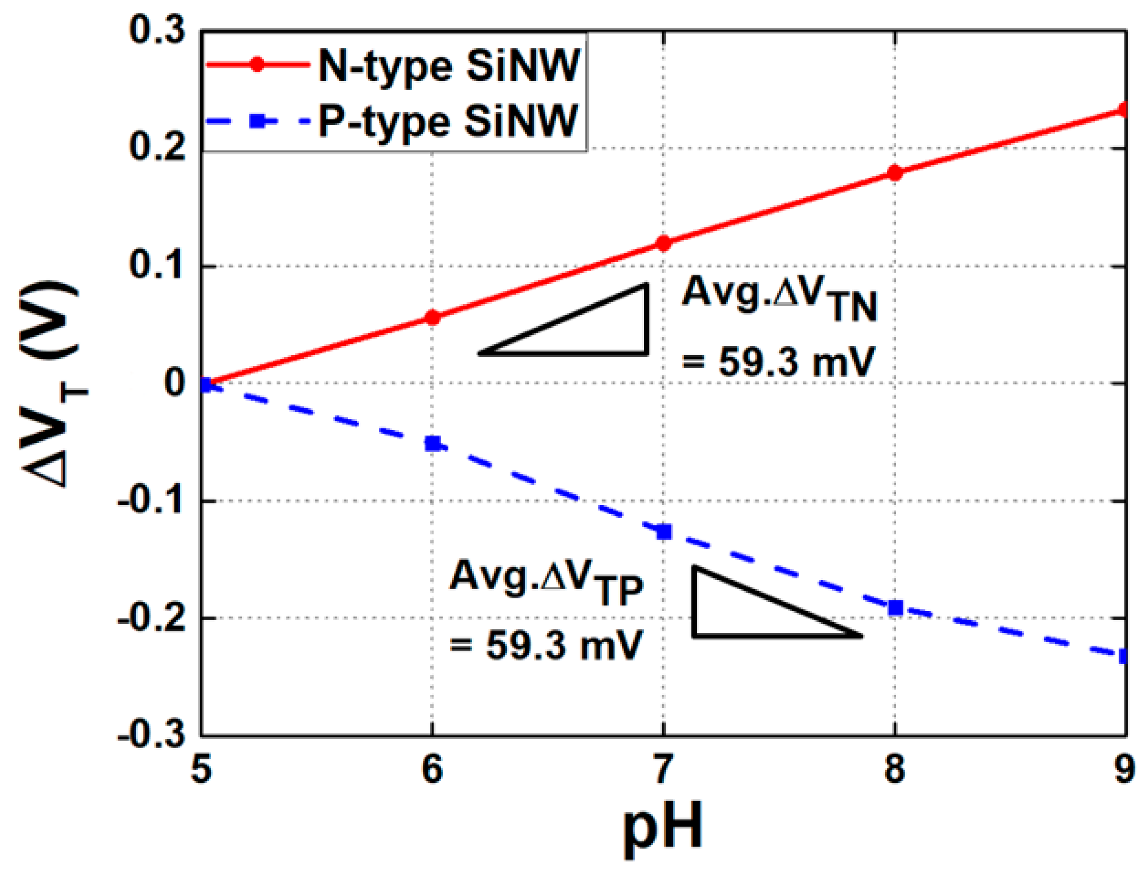
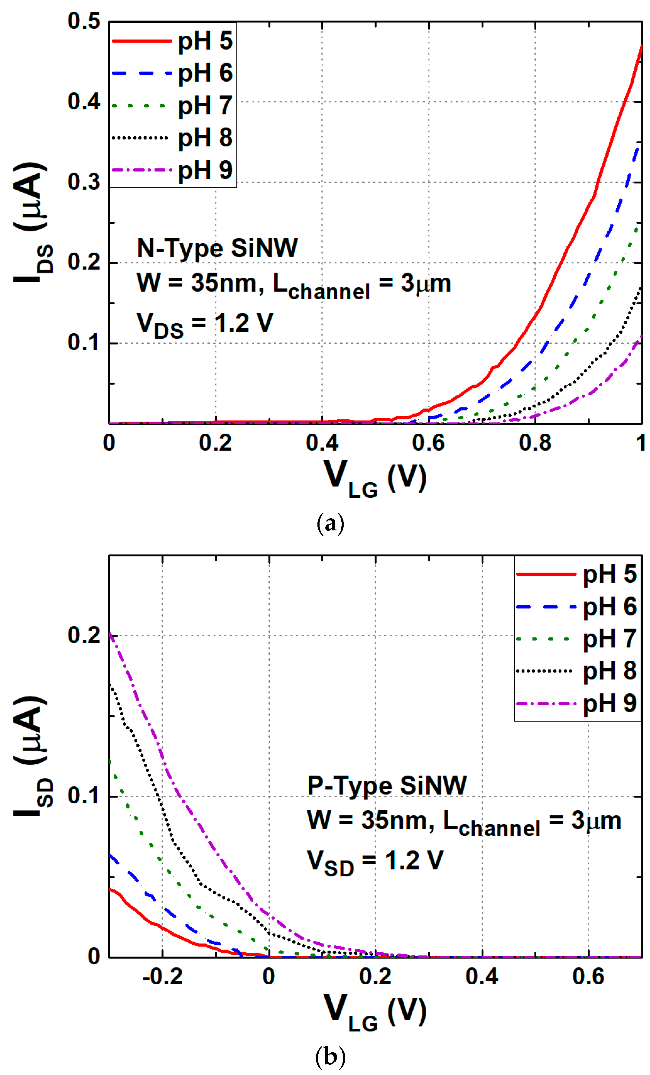
3. SiNW ISFET as a Hydrogen Ion Sensor

The field effect that governs the operation of basic CMOSFETs also applies to SiNW biosensors. In an N-type ISFET, the source and drain regions are doped with N-type material, whereas the substrate consists of P-type material. As a complementary device, a P-type FET is fabricated using opposite-type dopants. The electrical properties of a SiNW ISFET are controlled by the gate voltage, which modulates channel conductance. For an N-type SiNW, the conductance of an ISFET decreases when the carrier is depleted by applying a low positive gate voltage, whereas it increases as the carrier is collected by applying a higher positive voltage. Due to the opposite polarity of carriers in N-type and P-type devices, the VTH responds to pH concentration changes in reverse directions. Specifically, at lower pH levels (a smaller number of negatively charged ions), the gate of N-type SiNW collects more electrons in the channel region, lowering VTH. On the other hand, in a P-type SiNW, a lower pH level inhibits hole collection, increasing VTH. The electric field generated by ion binding at the gate functions similarly to an externally applied voltage. As illustrated in Figure 6, these characteristics enable SiNW ISFETs to function as electrical-based sensors, and they have been used as biosensors in various studies [92,117,118].
A SiNW ISFET, a representative example of a FET-based biosensor, operates by controlling the conductance of the semiconductor channel through the gate voltage, thereby electrically connecting the source and drain. In pH concentration sensing, when the -NH2 group reaches the surface of the gate dielectric layer, it is either protonated to -NH3 or the surface is deprotonated to -SiO-, depending on the pH concentration. As a result, the interaction between the charged target molecule and the surface-immobilized receptor generates an electric field that influences the conductivity of the SiNW ISFET channel. When negatively charged target molecules bind to the receptors, positive carriers accumulate in the channel, whereas negative carriers accumulate when positively charged molecules bind. Therefore, as pH concentration increases, the VTH of the N-type SiNW ISFET increases, whereas the VTH of the P-type SiNW ISFET decreases, as shown in Figure 6. Since the drain currents (ID) are affected by VTH, similar to the conventional FETs, the transfer characteristics of a SiNW ISFET depend on pH concentration. Figure 7a,b illustrate the ID of the N-type and P-type SiNW ISFETs versus gate voltages shown for different pH concentrations, respectively. Using these characteristics, many studies in the literature have investigated the design of readout circuits [97,116].

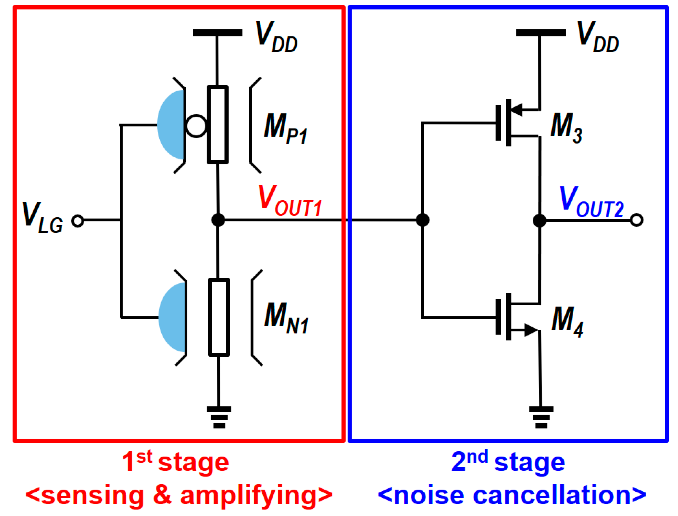
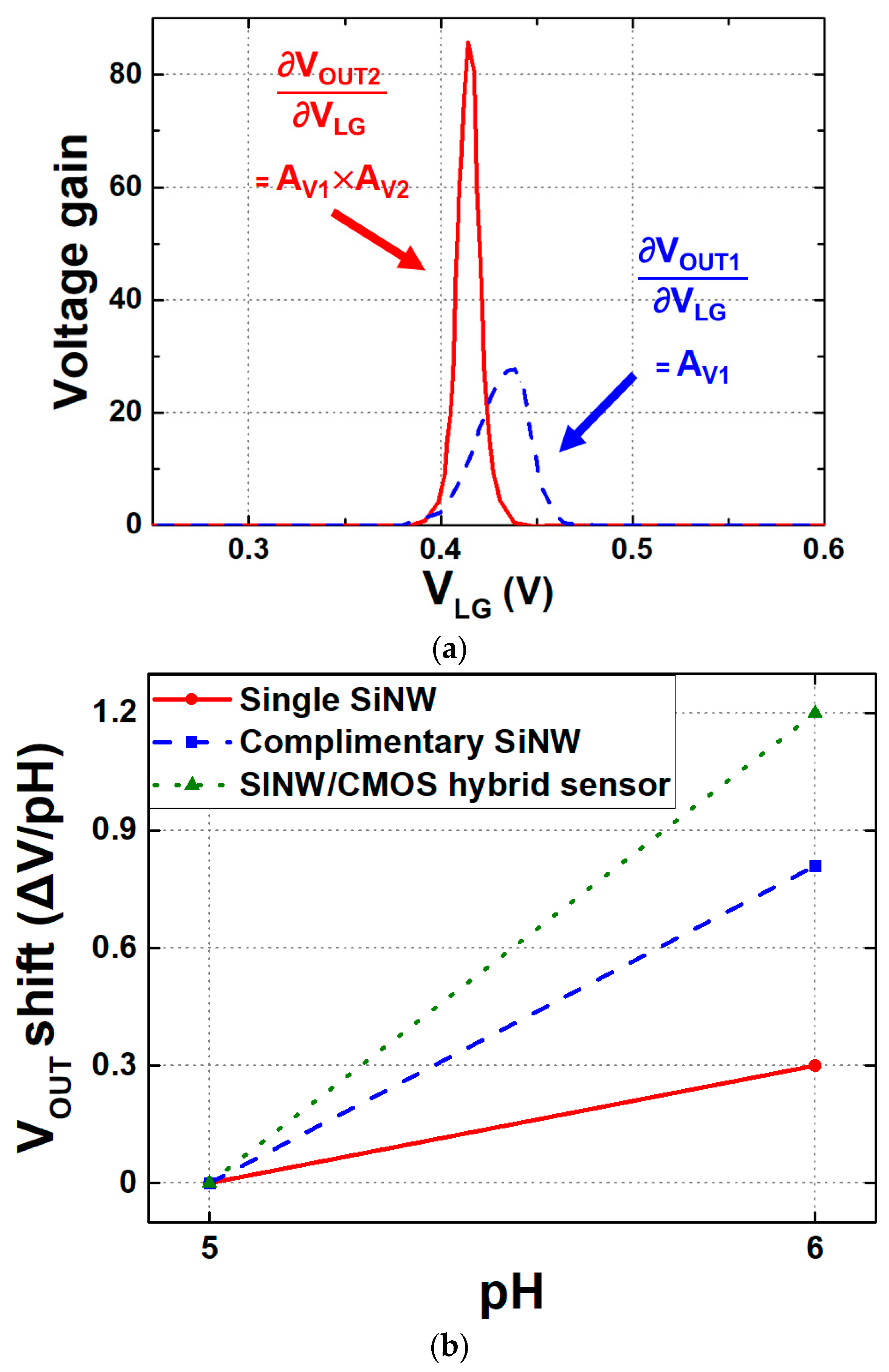
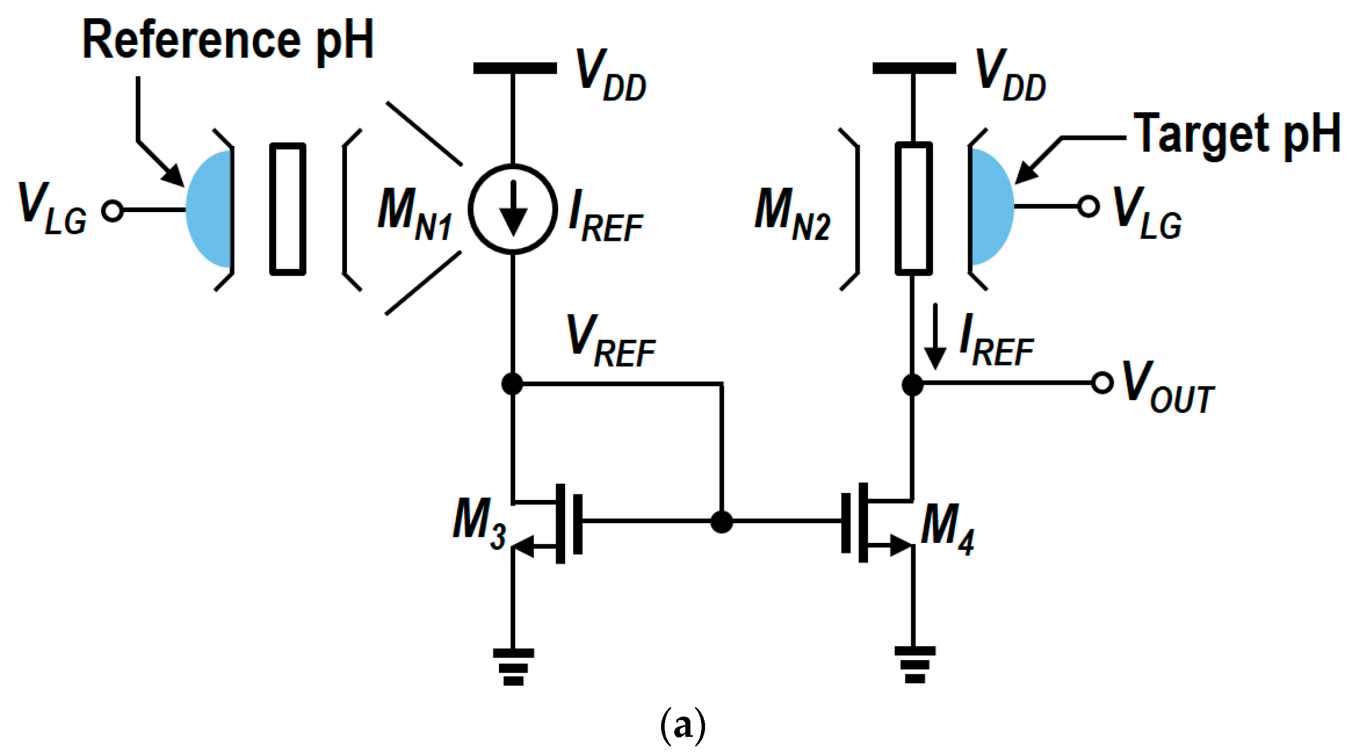
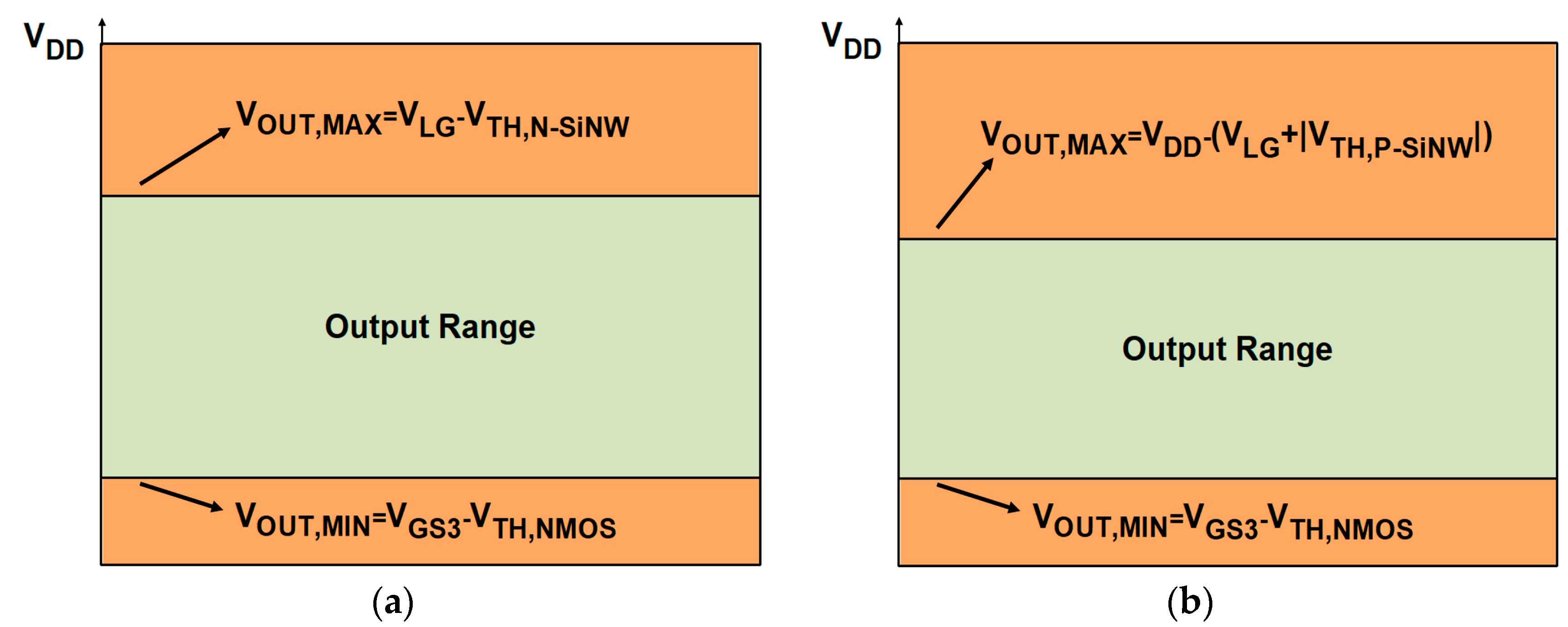
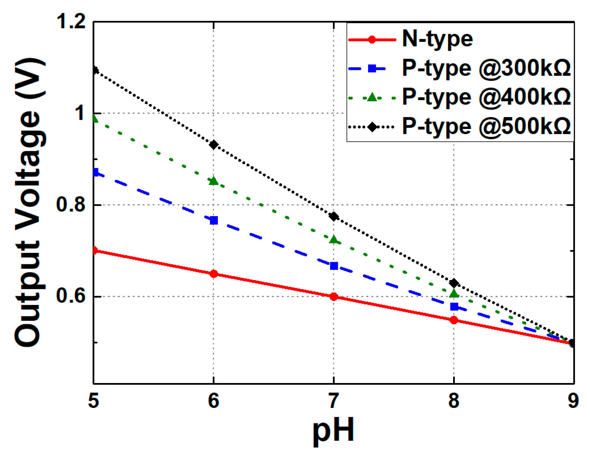
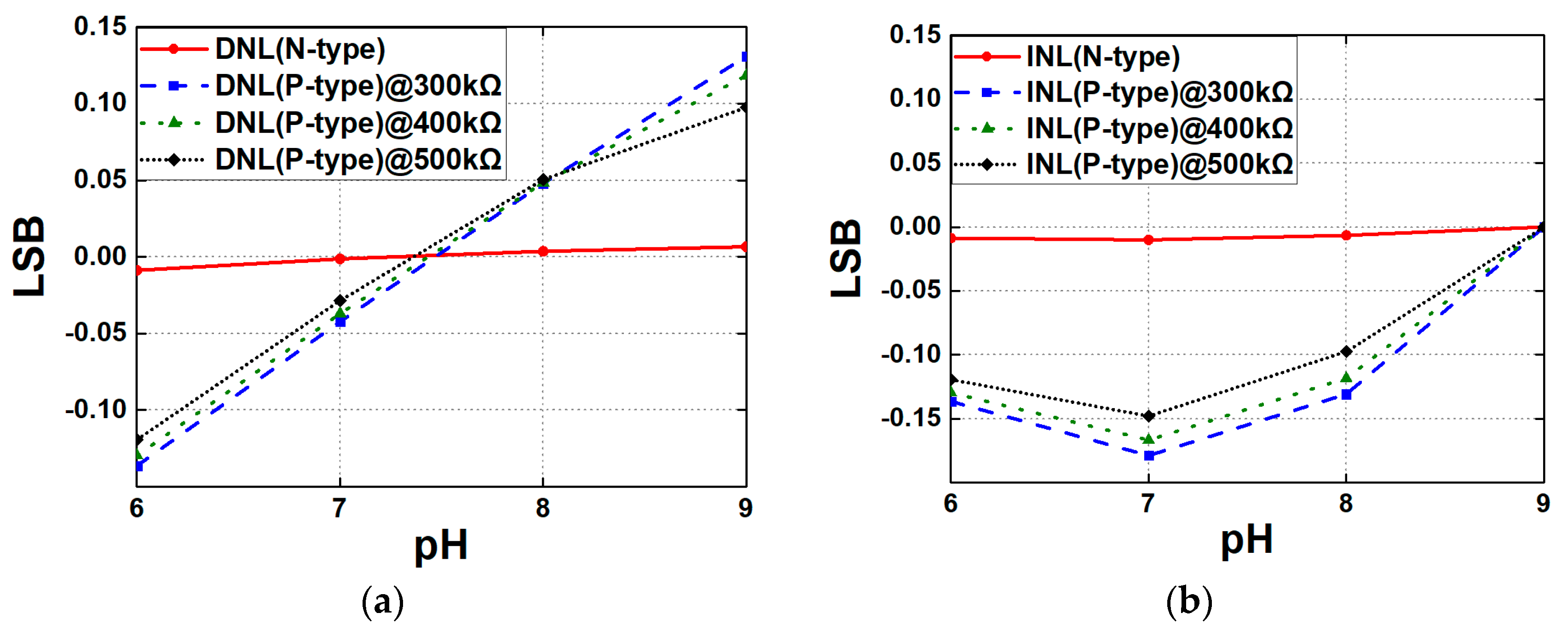
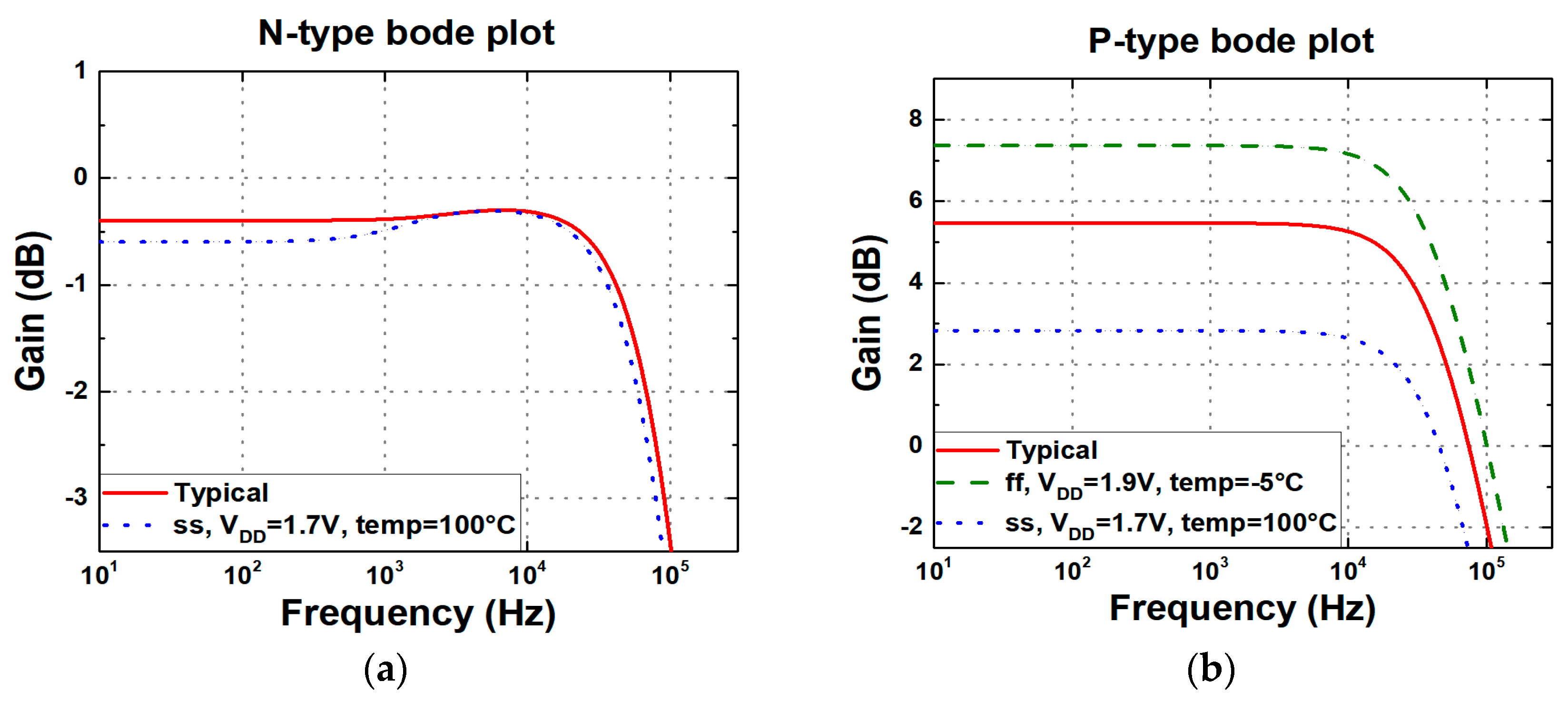
4. Circuit Design and Analysis of Readout Circuits

This section provides a comprehensive analysis of SiNW ISFET-based readout circuits, including conventional designs, SiNW/CMOS hybrid architectures, and current-mirror-based configurations. The discussion highlights their design methodologies, advantages, and key performance trade-offs to identify the most suitable approach for specific biosensor applications.
To utilize SiNW ISFETs as biosensors, various readout schemes have been proposed to detect changes in the VTH of SiNW ISFETs under different pH concentrations (See Figure 8). Among them, the conventional SiNW ISFET circuit [8] employs a single-gate structure to detect pH changes by monitoring shifts in VTH of the nanowire (Red box in Figure 8). Its design is simple and cost-effective, making it suitable for basic pH sensing applications. The improvement in sensitivity of this circuit is somewhat limited; however, small changes in VTH result in relatively small differences in its current response.
The sensitivity-enhanced SiNW ISFET circuit [96] builds upon the conventional design by introducing a dual-gate configuration, which enhances electrostatic control over the nanowire and results in larger VTH shifts (ΔVTH1 < ΔVTH2, where #1 refers to the conventional circuit and #2 refers to the sensitivity-enhanced SiNW ISFET circuit). Despite this improvement, the current sensitivity remains near the same (ΔI1 = ~ΔI2), and consequently, the output voltage sensing margin in the actual readout circuitry does not provide significant advantages (ΔVOUT1 = ~ΔVOUT2). Furthermore, the logic threshold voltage (VLTH), defined as the voltage level at which the logic state transitions, is determined by the VTH shifts in N-type and P-type SiNW FETs. VLTH is expressed as shown in Equation (1), which combines the VTH shifts in both N-type and P-type transistors. These shifts, driven by pH-induced surface charge changes, make VLTH a critical metric for assessing the stability and logic accuracy of SiNW-based circuits. Moreover, both circuits are susceptible to power supply noise, which may propagate during signal processing and compromise data acquisition reliability. These challenges underscore the importance of mitigating noise amplification and enhancing sensitivity in SiNW biosensor circuits.
V LTH = V NTH + V PTH 2 .
Building on these observations, a more advanced readout architecture is required to enhance sensing performance and improve noise robustness. Among various approaches, integrating SiNW ISFETs with CMOS technology presents a promising solution, combining the advantages of both platforms. To overcome the challenges of limited output voltage sensing margin and noise susceptibility, a hybrid biosensor circuit has been proposed [97]. By leveraging the strengths of both SiNW and CMOS devices, this approach enhances sensitivity while effectively suppressing noise, leading to improved overall sensor performance. The hybrid approach maximizes signal detection and minimizes noise, ensuring reliable biosensor operation.
The SiNW/CMOS hybrid circuit employs a two-stage architecture, as illustrated in Figure 9. In the first stage, the SiNW sensor detects and amplifies the initial signal by leveraging the complementary operation of N-type and P-type SiNWs to generate an amplified output voltage (ΔVOUT1), as shown in Figure 10. This complementary operation ensures that the sensing signals are reinforced, leveraging the voltage transfer characteristics of the SiNW sensor to achieve initial amplification. The second stage is designed to suppress supply noise by leveraging the opposite polarity in gain, further improving signal integrity.
The following section examines how this hybrid architecture achieves improved pH detection sensitivity and stabilizes the output by mitigating noise transfer. As pH concentration increases, the SiNW surface charge becomes more negative, inducing complementary VTH shifts: a positive shift in the N-type SiNW FET and a negative shift in the P-type SiNW FET. These shifts collectively drive a positive change in the logic threshold voltage (VLTH). The measured VLTH shift is approximately 50 mV per pH, closely matching the Nernst limit. This result confirms the effectiveness of the SiNW block in amplifying the output voltage (ΔVOUT1/ΔpH) in the first stage.
Figure 11a demonstrates how this shift translates into amplified output voltage sensitivity (ΔVOUT1/ΔpH) in the first stage. The complementary operation of N-type and P-type SiNW FETs not only shifts VLTH but also enhances the output voltage per pH change beyond the Nernst limit. This is achieved through the voltage gain (AV1) provided by the SiNW block, which enhances the signal at this initial stage. The amplified output voltage shift in the first stage (ΔVOUT1/ΔpH) serves as the foundation for the second stage of amplification. As illustrated in Figure 11a, this initial amplification is critical for achieving the overall high sensitivity of the SiNW/CMOS hybrid biosensor, which is further enhanced in the CMOS stage. These results emphasize the critical role of the SiNW block in boosting sensitivity, enabling precise detection of even minor pH variations.
The amplification process in the SiNW/CMOS hybrid biosensor can be mathematically expressed as follows:
Δ V OUT 1 Δ pH = Δ V OUT 1 Δ V LG · Δ V LG Δ V LT · Δ V LT Δ pH = A V 1 · 1 · Δ V LTH Δ pH ,
for the first stage, where AV1 represents the voltage gain of the SiNW block. In the second stage, the CMOS logic inverter further amplifies the signal as follows:
Δ V OUT 2 Δ pH = Δ V OUT 2 Δ V OUT 1 · Δ V OUT 1 Δ pH = A V 1 · A V 2 · Δ V LTH Δ pH .
Combining both stages, the overall sensitivity of the hybrid biosensor can be expressed as follows:
Δ V OUT 2 = A V 1 · A V 2 · Δ V OUT 1 .
This mathematical model highlights the synergistic amplification achieved through the combination of the SiNW and CMOS stages.
As illustrated in Figure 11b, the SiNW/CMOS hybrid biosensor exhibits a significant sensitivity improvement over conventional designs. This enhanced sensitivity results from the integration of the SiNW block and CMOS amplification stages, enabling the hybrid biosensor to achieve an output sensitivity of approximately 1.2 V/pH. This performance is markedly superior to that of the individual SiNW structure (0.3 V/pH) and the complementary SiNW block (0.81 V/pH). These results highlight the hybrid architecture’s ability to overcome the limitations of single-stage designs by leveraging dual-stage amplification for the detection of minor pH changes. Building on this enhanced architecture, it is anticipated that the circuit will be capable of generating highly sensitive output voltage signals even for minor pH variations.
To detect subtle biochemical changes, it is not only important to improve sensitivity but also to achieve a stable output while minimizing noise. In addition to delivering higher sensitivity, the hybrid SiNW/CMOS design increases the potential for robust noise suppression by using the CMOS inverter-type gain stage. Building on this concept, the following section explains how the hybrid biosensor effectively mitigates power supply fluctuations and maintains consistent performance under various operating conditions.
The SiNW/CMOS hybrid biosensor excels in noise reduction by integrating the CMOS inverter gain stage directly into the SiNW biosensor. With careful optimization of the second-stage gain, the average power supply noise can be suppressed, resulting in reduced voltage fluctuations. This design minimizes interference from the bulk electrolyte and the electrolyte–oxide interface, ensuring that noisy bio-signals are effectively filtered out. Experimental observations and TCAD simulations have validated the biosensor’s ability to produce clean, stable output signals in the presence of supply noise. This robustness across various environmental conditions underscores the reliability of the hybrid biosensor, establishing it as a practical platform for applications requiring precise biochemical sensing.
In addition to noise suppression and stability, another critical aspect of biosensor performance is the ability to provide accurate and reliable detection under varying conditions. These capabilities are key requirements for advanced applications such as genetic screening, early disease diagnostics, and personalized medicine. Thanks to its label-free detection method, there is no need for complex chemical labeling, which simplifies the sensing process while maintaining high accuracy. However, whereas the SiNW/CMOS hybrid biosensor significantly improves noise immunity, its ability to ensure precise detection across different environmental and process conditions remains a challenge. Variability in VTH shifts and signal amplification can impact sensing performance, requiring further advances in circuit design to improve precision, linearity, and DR.
In order to address these challenges, advanced readout circuit architectures have been explored to enhance signal processing and detection accuracy. Among these, current-mirror-based circuits offer a promising solution for improving both performance and functionality in SiNW ISFET biosensors. By leveraging a reference pH level for comparison, this approach enables precise detection of target pH concentrations by analyzing differences in VOUT caused by VTH shifts. This method ensures that the output voltage reflects only the VTH shifts, minimizing interference from other parameters such as mobility variations and background noise.
These circuits operate by comparing the reference pH level with the target pH concentration and detecting differences in output voltage (VOUT) as a result of VTH shifts. By isolating the voltage response to VTH variations, this method significantly reduces interference from external factors such as carrier mobility variations and background noise, leading to more reliable pH detection [98].
In this approach, the SiNW operates in the saturation region, where the ID is governed by the MOSFET equation, as depicted in Equation (5). As VTH changes with pH concentration, the corresponding variations in overdrive voltage result in proportional changes in ID, enabling precise pH sensing through current modulation. In this equation, μFE represents the mobility of the carriers in the SiNW, Cox is the unit oxide capacitance, and VG and VS are the gate and source voltages of the SiNW. The current equation for a SiNW ISFET follows the standard MOSFET saturation region equation. Assuming the SiNW operates in the strong inversion region with negligible mobility degradation due to surface roughness, the current equation can be derived as follows:
I SIN W = 1 2 μ FE C ox W eff L V G V s V T . SIN W 2 .
To evaluate the effectiveness of current-mirror-based readout circuits, key performance characteristics such as output range, sensitivity, linearity, and supply noise must be considered. The output range determines the maximum DR of the readout circuit. If the output range is too narrow, the DR may be limited, leading to distortion in the pH-dependent output. Even with a sufficiently wide output range, low sensitivity can be a limiting factor, making it difficult to detect low pH concentrations. For example, when interfacing with an analog-to-digital converter (ADC), insufficient sensitivity prevents setting a sufficiently small least-significant bit (LSB) for high-resolution operation. Additionally, lower sensitivity amplifies the perceived impact of output noise. As illustrated in Figure 12, a higher sensitivity readout circuit maps output noise to a narrower input range (Figure 12a), whereas lower sensitivity leads to a wider input range (Figure 12b) under the same output noise conditions. This observation highlights the critical trade-off between sensitivity and noise in biosensor design, emphasizing the need for careful noise management in high-precision applications.
For a comparative comparison and analysis, various performance metrics were evaluated using BSIM3 (Level-49) SiNW ISFET models and TSMC 180 nm standard CMOSFET models in a circuit simulator [119,120]. VTH was extracted from the IDS − VLG characteristic curves at VDS = 2 V. Both the N-type and P-type SiNW ISFETs were designed with the same W/L ratio of 200 nm/3 µm, and the CMOSFETs were also designed with the same W/L ratio of 1.5 µm/2 µm. For the operation of CMOS models in the readout circuits, the supply voltage (VDD) was set to 1.8 V [12].
Figure 13a,b illustrate the N-type and P-type readout circuits [12,98], respectively. The N-type readout circuit employs an N-type SiNW ISFET as a sensor and primarily uses a current-mirror configuration. The VTH of the SiNW ISFET changes in response to variations in the input pH concentrations, which subsequently changes the VOUT. As all of the SiNW ISFETs and CMOSFETs in each readout circuit are designed and biased to operate in saturation, the output range is limited by the boundaries between the triode and saturation regions of each transistor. In the case of the N-type readout circuit (Figure 13a), the conditions for the saturation region of M3, M4, MN1, and MN2 are given by the following Equations (6) and (7). Equation (8) is the condition for enabling the operation of SiNW ISFETs.
V REF V TH , NMOS < V OUT .
V LG V TH,N-SiNW < V DD .
V LG V TH,N-SiNW > V OUT .
As shown in Equations (6)–(8), the output range of the N-type readout circuit is limited by the overdrive voltage of M3, M4, MN1, and MN2. Figure 13b illustrates the P-type readout circuit, which is based on a P-type SiNW ISFET and employs a current-mirror configuration similar to the N-type counterpart. The VTH of the SiNW ISFET changes with pH variations, which determines the VOUT. Unlike the N-type circuit, a P-type SiNW ISFET is used as a sensor in the P-type readout circuit. The conditions under which NMOS transistors operate in saturation of the P-type readout circuit are identical to those in the N-type version. And the conditions under which a SiNW operates in the saturation region are shown in Equation (9).
V DD ( V LG + | V TH,N-SiNW | ) > V OUT .
Consequently, the output range of the P-type readout circuits is constrained by the saturation conditions of NMOSFETs and SiNW ISFETs, as illustrated in Figure 14. In the simulation setup, the values of VDD, VLG,P-SiNW, VTH,N-SiNW, and VTH,P-SiNW were 1.2, 0.35, 0.35, and 0.1 V, respectively. A comparison of the output ranges between the N-type and P-type ISFETs reveals that the output range of the P-type ISFET is comparatively smaller. This is mainly due to differences in VTH and the resulting VSAT levels. VSAT in a MOSFET refers to the drain-source voltage (VDS) at which the device enters saturation, where ID becomes stabilized and largely independent of VDS.
Even if the output range is large enough, the sensing performance is still significantly influenced by the sensitivity of the given readout scheme. A low sensitivity can lead to an increased influence of noise on the output node, thereby corrupting the quality of the output. Consequently, it is essential to analyze and optimize the sensitivity of the readout circuitry, as well as the output range and linearity. In the case of the N-type readout circuits, there is no amplification function as the M2 and M4 transistors act as source followers. Moreover, as M4 is not an ideal current source, it provides a voltage gain of less than unity. In [98], the sensitivity of the N-type readout circuit is approximately 50 mV/pH, which is similar to the variations in V TH of the SiNW ISFET. In contrast, in the P-type readout circuit, SiNW ISFETs serve as a common-source amplifier with an NMOS current source as its load. Accordingly, the gain of the circuit can be modulated by the output resistance (ROUT). In [12], the sensitivity of the P-type readout circuit increases by approximately 90%, depending on the ROUT.
Figure 15 shows the VOUT results for the N-type and P-type readout circuits. As illustrated, the N-type readout circuit exhibits a fixed and relatively low sensitivity due to the absence of an amplification stage. In contrast, the P-type readout circuit exhibits a significant improvement in sensitivity since the common-source stage provides signal gain. According to the simulations, adjusting the output resistance from 300 to 500 kΩ increases the sensitivity from 93 to a maximum of 149 mV/pH. In addition, the resistance can be optimized for the different input impedances of the subsequent stage. Regarding the selection of the optimal resistance of ROUT, the following aspects may be considered: First, increasing the ROUT of the P-type readout circuit improves the sensitivity. In many cases, a higher sensitivity is preferred, but at the same time, a high sensitivity may put limitations on the range of VOUT, reducing the DR of readout circuits. Furthermore, increasing ROUT potentially degrades the linearity characteristics of readout systems, which will be discussed in more detail in the following paragraph.
Linearity is an essential characteristic in readout circuits. Using an ADC after readout circuits can lead to increased quantization noise due to nonlinearity, thereby resulting in a decrease in SNR. Changes in VOUT of the N-type readout circuit in response to the changes in VTH of a SiNW due to pH variations can be calculated by Equations (10) and (11). Equation (11) shows that VOUT is linear with respect to the VTH of SiNW.
B SiN W 2 ( V LG V REF V TH , REF ) 2 = B SiN W 2 ( V LG V OUT V TH , TARGET ) 2 .
V OUT = V REF + V TH V TH , TARGET = V REF + Δ V TH .
As demonstrated in Equations (10) and (11), the final VOUT is determined by pH variations detected by the sensor. The reference voltage (VREF) is a constant voltage with respect to VTH of the MOSFET at the reference pH, serving as a baseline for pH measurement. The conduction parameter of a SiNW (BSiNW) is associated with mobility, gate capacitance, and device dimensions. The change in the VOUT of the P-type readout circuit is expressed in Equation (13) and is not linear to VTH of a SiNW.
V OUT = V REF + I OUT R OUT = V REF + ( I TARGET I REF ) R OUT
V OUT = V REF + R OUT B SiN W   · Δ V TH 2 ( 2 ( V DD V LG ) 2 | V TH . REF | + Δ V TH )
In Equations (12) and (13), I TARGET denotes the target current in the context of the circuit being described. This is defined as the current that flows through the SiNW ISFET when it is exposed to the target pH level or specific analyte concentration being measured. This current is used to determine the sensor’s response, as it reflects the changes in the sensor’s electrical properties due to the interaction with the target molecules or ions. The ITARGET value is commonly compared to the reference current (IREF) to generate a corresponding output signal. The detailed derivation of Equation (13) is shown in Appendix A.
As demonstrated in Figure 16, the differential nonlinearity (DNL) and integral nonlinearity (INL) characteristics of the N-type and P-type readout circuits are exhibited under varying ROUT. Figure 16a illustrates that the N-type readout circuit demonstrates excellent linearity, exhibiting DNL values that are nearly equal to 0.009 LSB. In contrast, the P-type readout circuit shows considerably higher DNL values, reaching up to 0.13 LSB, suggesting a heightened risk of distortion or nonlinearity in the output signal. Figure 16b illustrates the INL values, which represent the cumulative deviations from ideal linearity across the entire output range. The N-type circuit demonstrates favorable INL performance, with values approximating 0.01 LSB, thereby indicating effective maintenance of overall linearity. In contrast, the P-type circuit exhibits considerably higher INL values, reaching up to 0.18 LSB and indicating a significant drawback in comparison with the N-type circuit. These findings imply that both circuits present their own advantages for pH-sensing applications. The N-type readout circuit, which exhibits superior linearity and minimal distortion, may be more suitable for applications where high accuracy and precision are required. On the other hand, the P-type circuit can provide enhanced sensitivity but may require additional calibration or tuning to offset its nonlinearity.
In addition to linearity considerations, the ability of a readout circuit to reduce power supply noise is a critical aspect of its performance, as this noise can significantly impact measurement accuracy. The current-mirror-based readout circuitry reviewed earlier generates single-ended outputs rather than differential signals, making it more susceptible to power supply fluctuations. In practical situations, a power supply includes unwanted fluctuations in addition to a DC voltage, and readout circuits may be sensitive to noise, which can degrade an SNR. Therefore, the supply noise dependence on VOUT should be evaluated, and it can be calculated from a small-signal analysis. Equations (14) and (15) represent the changes in VOUT resulting from supply voltage noise in the N-type and P-type readout circuits, respectively. By taking a partial derivative of VOUT with respect to VDD, it is possible to obtain the following equations. These equations were derived using the small-signal models in Figure 13a,b, and the process is described in detail in Appendix B.
For the N-type,
d V OUT d V DD = 1 1 + r o . SiN W r on + g m . SiN W   ·   r o . SiN W 1 g m . SiN W   · r o . SiN W .
For the P-type,
dV OUT dV DD = ( g m . SiN W   ·   r o . SiN W + 1 r o . SiN W ) ( r on | | r o . SiN W ) g m . SiN W   ·   ( r on | | r o . SiN W ) .
In Equations (14) and (15), gm.SiNW represents the transconductance of a SiNW ISFET, which denotes the rate of change in ID with respect to the gate voltage. The parameter ron indicates the on-resistance of the NMOS when the transistor is in the ON state. Meanwhile, ro.SiNW represents the output resistance of a SiNW ISFET, which characterizes the resistance associated with the change in VDS when ID remains constant. These parameters have a considerable impact on the circuit’s sensitivity to power supply noise, as well as its overall linearity and performance.
In the N-type readout circuits, the supply noise does not directly appear at the output as long as SiNW ISFETs are in the saturation region. Because the core structure is configured as a cascode stage, the impedance looking into the circuit from the power supply is boosted by the product of gm of the SiNW ISFET and ro of M4 in Figure 13a, reducing the impact of noise. Conversely, in P-type readout circuits, the power supply noise is amplified by the gm.SiNW due to the common-source configuration. This noise is converted into a current and is multiplied by ROUT, resulting in the VOUT. Figure 17 and Figure 18, respectively, present the Bode plot of the N-type and P-type readout circuits and the output voltage waveform under power supply noise conditions. For the Bode plot simulation, a load capacitor of 10 pF was incorporated at the circuit output to ensure stability and to account for realistic loading conditions. Each simulation was conducted under PVT corner conditions, selecting both typical and worst-case scenarios. The PVT simulations encompassed a total of 27 cases, with transistor process corners (tt, ss, and ff), supply voltages (VDD = 1.7 V, 1.8 V, and 1.9 V), and temperatures (−5 °C, 27 °C, and 100 °C) varied. In Figure 17, only the worst cases were selected for visualization. Figure 18 illustrates the worst-case scenarios—where the transistor operates in ss or ff process corners with VDD = 1.7 V/1.9 V and temperature = −5 °C/100 °C—were highlighted. The power supply noise was modeled as a sinusoidal waveform with an amplitude of ±10% relative to VDD. In the N-type readout circuit, the supply voltage noise decreases to a 1% level. However, in the P-type readout circuit, the noise is amplified by more than twice, and the noise gain increases as ROUT becomes larger. Therefore, as the sensitivity of the P-type readout circuit increases, its dependence on power supply noise also grows. Additionally, it is highly sensitive to PVT variations, and in worst-case scenarios, pH sensing fails to function properly.
The N-type and P-type readout circuits each present distinct trade-offs in terms of linearity, sensitivity, and noise resilience. While the N-type circuit ensures superior linearity (0.009 LSB/0.01 LSB) and noise immunity (1.2 mV variation), its sensitivity (~50 mV/pH) is limited due to the absence of an amplification stage. In contrast, the P-type circuit provides higher sensitivity (up to 149 mV/pH) but exhibits increased nonlinearity (0.13 LSB/0.18 LSB) and greater susceptibility to supply noise (343 mV variation). These trade-offs indicate that N-type circuits are more suitable for stability, while P-type circuits are better suited for applications requiring enhanced sensitivity.

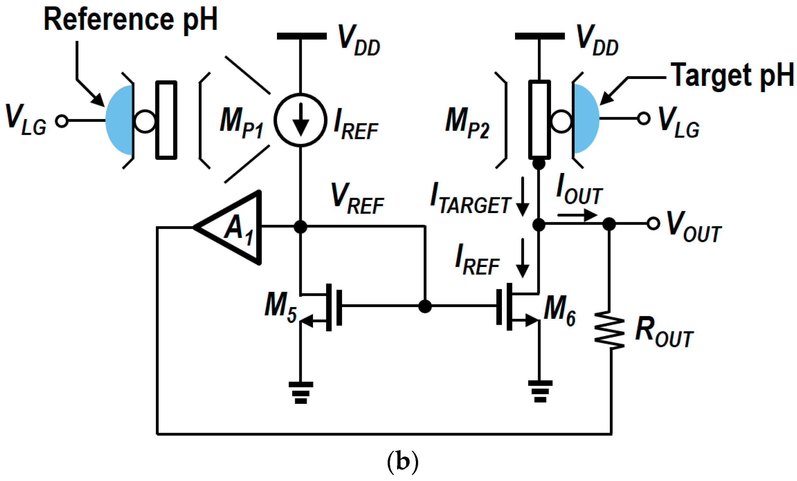
5. Modified N-Type Readout Scheme

A comparative analysis and the results presented in the previous sections suggest that the N-type readout circuit exhibits good linearity and low dependence on power supply noise, but it is unable to control gain and sensitivity. On the other hand, the P-type readout circuit can adjust sensitivity but suffers from low linearity and high dependence on supply noise. To address the limitations of these readout circuits, the modified N-type readout circuit is proposed as a promising future direction in biosensor designs. As illustrated in Figure 19, the modified N-type readout circuit integrates an op-amp with a resistive feedback network (R1, R2). This integration enables precise control over sensitivity while maintaining the superior linearity and noise immunity of the conventional N-type design. This configuration enables precise adjustment of sensitivity through the ratio of R1 to R2, enhancing the circuit’s sensitivity without compromising linearity or introducing noise issues. In comparison to the P-type readout circuit, which allows for sensitivity adjustment but is highly susceptible to noise, this modified design retains the noise robustness of the N-type circuit while significantly enhancing detection capabilities.
This enhanced sensitivity is particularly advantageous in real-time biosensor applications, where the precise detection of small pH concentration changes is crucial. By effectively addressing the trade-offs between sensitivity, noise immunity, and linearity, the modified N-type readout circuit not only resolves the limitations of both N-type and P-type designs but also ensures high precision in pH detection. The modified circuit was designed using the same process as the N-type and P-type readout circuits discussed earlier.
V OUT = ( 1 + R 2 R 1 ) V O R 2 R 1 V REF = V REF + ( 1 + R 2 R 1 ) ·   Δ V TH .
V O = V REF + Δ V TH .
As indicated by Equations (16) and (17), the final VOUT is determined by the pH variation detected by the sensor and is an amplified value produced by the operational amplifier A2. The intermediate output voltage (VO), which corresponds to the source voltage of MN4, represents the measured pH level and plays a crucial role in determining the final output voltage. The value of VO is expressed as the sum of the reference voltage (VREF), which corresponds to a reference pH level, and the threshold voltage shift (ΔVTH) caused by the pH variation. ΔVTH indicates the change in the threshold voltage at the target pH relative to the reference pH. VREF is a fixed voltage related to the threshold voltage of the MOSFET at the reference pH and serves as a baseline for pH measurement. Figure 20 presents the simulation results of the change in output voltage with pH concentration when the ratio of R1 and R2 is 1, 2, or 3. The sensitivity of the proposed circuit was enhanced from 87 mV/pH to 172 mV/pH.
In scenarios where sensitivity is paramount, it is essential to regard noise as an external factor that can influence circuit performance. As previously discussed, the current-mirror type readout circuits do not utilize differential structures that facilitate supply noise cancelation. In the modified N-type readout, the circuit may exhibit sensitivity to supply noise, which can cause fluctuations in the output voltage. Therefore, the supply noise dependence of the VOUT should be carefully examined through the implementation of appropriate small-signal analysis. Additionally, as there is no DC current flowing into the op-amp, the impact of supply noise on the output can be described by Equation (14). Since the modified N-type readout circuit adopts the structure of the existing N-type design, Equation (13) may also be applied. As mentioned earlier, the cascode structure of the N-type readout circuit provides inherent shielding against supply noise, ensuring that the output voltage remains largely insensitive to such variations. Figure 21a illustrates the concept of supply noise immunity in the modified N-type readout circuit. The cascode configuration effectively shields the circuit from power supply noise, reducing its impact on the output voltage. Figure 21b,c present the PVT corner simulation output voltage waveforms under power supply noise conditions at temperatures of −5 °C and 100 °C, respectively. Under the same percentage VDD variation as in Figure 18, the peak-to-peak output voltage variations for the modified N-type readout circuit were observed to be about 5 mV, which is comparable to the peak-to-peak output voltage variations seen in the current-mirror-based N-type readout circuit. Figure 22 presents the Bode plot of the modified circuit. The PVT simulation results indicate that the variations in gain and bandwidth remained within 2% compared to the typical case, even under worst-case conditions; therefore, they were not included in the figure. Finally, Table 4 summarizes the key differences between the two current mirror-based readout circuits and the modified readout circuit.
The modified readout circuit demonstrates high linearity and excellent noise immunity, making it a promising design for various biosensor applications. However, design constraints, such as the accuracy of resistors and the offset voltage of op-amps, may potentially affect resolution. These limitations could be addressed through alternative configurations, such as replacing resistors with switched-capacitor structures, which are expected to further enhance the circuit’s performance. With these improvements, the proposed circuit could offer a more robust and reliable solution for precise biochemical sensing across diverse applications.

6. Conclusions

This paper presents a comprehensive review of SiNW ISFET-based readout circuits designed for biosensor applications. First, the fabrication methods and unique characteristics of SiNW ISFETs are explained, followed by a discussion of the performance metrics associated with different types of readout circuits. The performance parameters, including dynamic (output) range, sensitivity (gain), linearity, and supply noise immunity, are investigated for the conventional types of readout circuits. In addition, the properties and features of SiNW/CMOS hybrid and current-mirror-based readout circuits are investigated with a detailed analysis.
Based on these findings, the notion of a modified N-type readout circuit is introduced as a prospective future direction. By addressing key limitations in existing designs, this approach underscores the potential for optimizing biosensor performance. Further research is essential to validate the expected advantages, refine its implementation, and ensure its effectiveness in a variety of practical applications. These efforts will lay the foundation for the development of more reliable and versatile biosensor technologies.

Author Contributions

Conceptualization, J.J., I.S. and D.H.K.; methodology, J.J. and H.M.; software, J.J. and S.K.; validation, H.M., I.S. and D.H.K.; formal analysis, J.J. and H.M.; investigation, J.J. and S.K.; resources, H.M. and D.H.K.; data curation, S.S. and I.S.; writing—original draft preparation, J.J., S.S. and I.S.; writing—review and editing, I.S. and D.H.K.; visualization, J.J. and S.S.; supervision, I.S. and D.H.K.; project administration, D.H.K.; funding acquisition, H.M. and D.H.K. All authors have read and agreed to the published version of the manuscript.

Funding

This work was supported in part by the National Research Foundation of Korea (NRF) funded by the Korean Government (MSIT) under Grant RS-2023-00208661, 2019M3F3A1A02071845, and 2022M3I7A078936, and in part by the 2023 research fund of Kookmin University in Korea. In addition, this work was supported by Institute of Information & Communications Technology Planning & Evaluation (IITP) under the artificial intelligence semiconductor support program to nurture the best talents (IITP-2025-RS-2023-00253914) grant funded by the Korea government (MSIT). The EDA tool was supported by the IC Design Education Center (IDEC), Korea.

Institutional Review Board Statement

Not applicable.

Informed Consent Statement

Not applicable.

Data Availability Statement

No new data were created or analyzed in this study.

Conflicts of Interest

The authors declare no conflicts of interest. The funders had no role in the design of the study; in the collection, analyses, or interpretation of data; in the writing of the manuscript; or in the decision to publish the results.

Appendix A

This section provides a detailed development of Equation (13) used in Section 4. The purpose of this appendix is to provide an explanation of the thesis to better understand these equations for readers.
First, let IREF be the current when the PMOS has a reference threshold voltage (VTH,REF) and IREF can be expressed as in Equation (A1). In the reference situation, VSG = VDD − VLG and VTH = VTH,REF. Therefore, IREF can be rewritten as Equation (A2), and for convenience, letting VOV = (VDD − VLG) − |VTH,REF|, IREF is simplified as Equation (A3).
I REF = B SiN W 2 ( V SG | V TH | ) 2 .
I REF = B SiN W 2 ( V DD V LG | V TH , REF | ) 2 .
I REF = B SiN W 2 ( V OV ) 2 .
If we assume that the VTH has shifted by ΔVTH due to a change in pH, the effective threshold voltage will be |VTH,REF| − ΔVTH. The result is VSG − VTH, as shown in Equation (A4). This can be represented as Equation (A5), which when expanded becomes Equation (A6).
( V SG | V TH | ) SENSOR = { ( V DD V LG ) ( | V TH , REF | V TH ) } .
I TARGET = B SiN W 2 ( V OV V TH ) 2 .
I TARGET = B SiN W 2 { V OV 2 + 2 V OV V TH + ( V TH ) 2 } .
If the sensor produces an output voltage by the difference between ITARGET and IREF, then ITARGET-IREF can be represented as Equations (A7) and (A8).
I TARGET I REF = B SiN W 2 { V OV 2 + 2 V OV V TH + ( V TH ) 2 } B SiN W 2 ( V OV ) 2 .
I TARGET I REF = B SiN W V OV V TH + B SiN W 2 ( V TH ) 2 .
If the schematic assumes that the output node flows current (ITARGET − IREF) through ROUT for VREF, then Equation (A9) holds. Substituting Equation (A8) into Equation (A9) at this stage yields Equation (A10), which is consistent with Equation (13).
V OUT = V REF + I OUT R OUT = V REF + ( I TARGET I REF ) R OUT .
V OUT = V REF + R OUT B SiN W   · Δ V TH 2 ( 2 ( V DD V LG ) 2 | V TH . REF |   + Δ V TH ) .

Appendix B

This section provides a detailed development of Equations (14) and (15) used in Section 4. The purpose of this appendix is to facilitate the understanding of these equations, and we have presented the development in as much detail as possible.
First, the small-signal model of the circuit in Figure 13a to arrive at Equation (14). In the circuit in Figure 13a, the small-signal model for the output stage is shown in Figure A1a. From Figure A1a, the expression for the current flowing from VDD to VOUT can be written as Equation (A11), which can be simplified to Equation (A12). This is consistent with Equation (14).
d V OUT r on = g m . SiN W   ·   d V OUT + d V DD d V OUT r on , SiN W .
d V OUT d V DD = 1 1 + r o n . SiN W r on + g m . SiN W   ·   r o n . SiN W 1 g m . SiN W   · r o n . SiN W .
Figure 13b can be analyzed in a similar way. Figure A1b shows the small-signal model of the output stage in Figure 13b, and as before, an expression for the current flowing from VDD to VOUT can be formulated as Equation (A13). This can be simplified to look like Equation (A14), which is consistent with Equation (15).
d V OUT r on = g m . SiN W   ·   d V DD + d V DD d V OUT r op . SiN W .
dV OUT dV DD = ( g m . SiN W   ·   r o p . SiN W + 1 r o p . SiN W ) ( r on | | r op . SiN W )     g m . SiN W · ( r on | | r o p . SiN W ) .
Figure A1. Small-signal model in (a) N-type readout circuit and (b) P-type readout circuit.
Biosensors 15 00206 g0a1

References

  1. Shinwari, M.W.; Deen, M.J.; Landheer, D. Study of the electrolyte-insulator-semiconductor field-effect transistor (EISFET) with applications in biosensor design. Microelectron. Reliab. 2007, 47, 2025–2057. [Google Scholar]
  2. Suhito, I.R.; Koo, K.-M.; Kim, T.-H. Recent Advances in Electrochemical Sensors for the Detection of Biomolecules and Whole Cells. Biomedicines 2021, 9, 15. [Google Scholar]
  3. Tsai, H.-C.; Doong, R. A Simultaneous determination of pH, urea, acetylcholine and heavy metals using array-based enzymatic optical biosensor. Biosens. Bioelectron. 2005, 20, 1796–1804. [Google Scholar]
  4. Kumar, S.; Singh, R. Recent optical sensing technologies for the detection of various biomolecules: Review. Opt. Laser. Technol. 2021, 134, 106620. [Google Scholar]
  5. Nelson, R.W.; Nedelkov, D.; Tubbs, K.A. Biosensor chip mass spectrometry: A chip-based proteomics approach. Electrophoresis 2000, 21, 1155–1163. [Google Scholar] [CrossRef]
  6. Breuker, K.; Jin, M.; Han, X.; Jiang, H.; McLafferty, F.W. Top-Down Identification and Characterization of Biomolecules by Mass Spectrometry. J. Am. Soc. Mass Spectrom. 2008, 19, 1045–1053.6. [Google Scholar]
  7. Grieshaber, D.; MacKenzie, R.; Vörös, J.; Reimhult, E. Electrochemical Biosensors—Sensor Principles and Architectures. Sensors 2008, 8, 1400–1458. [Google Scholar] [CrossRef]
  8. Stern, E.; Klemic, J.F.; Routenberg, D.A.; Wyrembak, P.N.; Turner-Evans, D.B.; Hamilton, A.D.; LaVan, D.A.; Fahmy, T.M.; Reed, M.A. Label-free immunodetection with CMOS-compatible semiconducting nanowires. Nature 2007, 445, 519–522. [Google Scholar]
  9. Sharma, A.; AlGhamdi, W.S.; Faber, H.; Lin, Y.-H.; Liu, C.-H.; Hsu, E.-K.; Lin, W.-Z.; Naphade, D.; Mandal, S.; Heeney, M.; et al. Non-invasive, ultrasensitive detection of glucose in saliva using metal oxide transistors. Biosens. Bioelectron. 2023, 237, 115448. [Google Scholar]
  10. Ishikawa, F.N.; Chang, H.-K.; Curreli, M.; Liao, H.-I.; Olson, C.A.; Chen, P.-C.; Zhang, R.; Roberts, R.W.; Sun, R.; Cote, R.J.; et al. Label-free, electrical detection of the SARS virus N-protein with nanowire biosensors utilizing antibody mimics as capture probes. ACS Nano 2009, 3, 1219–1224. [Google Scholar]
  11. Liu, A. Towards development of chemosensors and biosensors with metaloxide-based nanowires or nanotubes. Biosens. Bioelectron. 2008, 24, 167–177. [Google Scholar] [CrossRef] [PubMed]
  12. Choi, S.; Kim, J.; Yoon, J.; Chae, I.; Choi, S.-J.; Kim, D.M.; Mo, H.S.; Kim, D.H. The Module of Gain-controllable Amplifier Readout Circuits based on Si Nanowire ISFET for Biochips for Optimization of Dynamic Range, Linearity, and Resolution. In Proceedings of the ESSDERC 2019-49th European Solid-State Device Research Conference (ESSDERC), Cracow, Poland, 23–26 September 2019. [Google Scholar]
  13. Lei, K.-M.; Mak, P.-I.; Law, M.-K.; Martins, R.P. CMOS biosensors for in vitro diagnosis—Transducing mechanisms and applications. Lab. Chip 2016, 16, 3664–3681. [Google Scholar] [CrossRef] [PubMed]
  14. Li, H.; Li, D.; Chen, H.; Yue, X.; Fan, K.; Dong, L.; Wang, G. Application of Silicon Nanowire Field Effect Transistor (SiNW-FET) Biosensor with High Sensitivity. Sensors 2023, 23, 6808. [Google Scholar] [CrossRef] [PubMed]
  15. Numnuam, A.; Thavarungkul, P.; Kanatharana, P. An amperometric uric acid biosensor based on chitosan-carbon nanotubes electrospun nanofiber on silver nanoparticles. Anal. Bioanal. Chem. 2014, 406, 3763–3772. [Google Scholar] [CrossRef] [PubMed]
  16. Thriveni, G.; Ghosh, K. Advancement and Challenges of Biosensing Using Field Effect Transistors. Biosensors 2022, 12, 647. [Google Scholar] [CrossRef]
  17. Li, H.; Liu, X.; Li, L.; Mu, X.; Genov, R.; Mason, A.J. CMOS Electrochemical Instrumentation for Biosensor Microsystems: A Review. Sensors 2017, 17, 74. [Google Scholar] [CrossRef]
  18. Samuel, V.R.; Rao, K.J. A review on label free biosensors. Biosens. Bioelectron. X 2022, 11, 100216. [Google Scholar] [CrossRef]
  19. Nair, P.R.; Alam, M.A. Performance limits of nanobiosensors. Appl. Phys. Lett. 2006, 88, 233120. [Google Scholar] [CrossRef]
  20. Li, Z.; Chen, Y.; Li, X.; Kamins, T.I.; Nauka, K.; Williams, R.S. Sequence-specific label-free DNA sensors based on Silicon Nanowires. Nano Lett. 2004, 4, 245–247. [Google Scholar] [CrossRef]
  21. Zhang, G.-J.; Zhang, L.; Huang, M.J.; Luo, Z.H.H.; Tay, G.K.I.; Lim, E.-J.A.; Kang, T.G.; Chen, Y. Silicon nanowire biosensor for highly sensitive and rapid detection of Dengue virus. Sens. Actuators B Chem. 2010, 146, 138–144. [Google Scholar] [CrossRef]
  22. Presnova, G.; Presnov, D.; Krupenin, V.; Grigorenko, V.; Trifonov, A.; Andreeva, I.; Ignateko, O.; Egorov, A.; Rubtsova, M. Biosensor based on a silicon nanowire field-effect transistor functionalized by gold nanoparticles for the highly sensitive determination of prostate specific antigen. Biosens. Bioelectron. 2017, 88, 283–289. [Google Scholar] [PubMed]
  23. Curreli, M.; Zhang, R.; Ishikawa, F.N.; Chang, H.-K.; Cote, R.J.; Zhou, C.; Thompson, M.E. Real-time, label-free detection of biological entities using nanowire-based FET. IEEE Trans. Nanotechnol. 2008, 7, 651–667. [Google Scholar]
  24. Chen, W.; Yao, H.; Tzang, C.H.; Zhu, J.; Yang, M.; Lee, S.-T. Silicon nanowires for high-sensitivity glucose detection. Appl. Phys. Lett. 2006, 88, 213104. [Google Scholar] [CrossRef]
  25. Gao, Z.; Agarwal, A.; Trigg, A.D.; Singh, N.; Fang, C.; Tung, C.-H.; Fan, Y.; Buddharaju, K.D.; Kong, J. Silicon Nanowire Arrays for Label-Free Detection of DNA. Anal. Chem. 2007, 79, 3291–3297. [Google Scholar] [CrossRef]
  26. Jayakumar, G.; Asadollahi, A.; Hellstrӧm, P.-E.; Garidis, K.; Östling, M. Silicon nanowires integrated with CMOS circuits for biosensing application. Solid States Electron. 2014, 98, 26–31. [Google Scholar]
  27. Schwierz, F. Graphene Transistors: Status, Prospects, and Problems. Proc. IEEE 2013, 101, 1567–1584. [Google Scholar]
  28. Zhan, B.; Li, C.; Yang, J.; Jenkins, G.; Huang, W.; Dong, X. Graphene Field-Effect Transistor and Its Application for Electronic Sensing. Small 2014, 10, 4042–4065. [Google Scholar]
  29. Wang, J. Carbonnanotube based electrochemical biosensors: A review. Electroanalysis 2005, 17, 7–14. [Google Scholar]
  30. Sotiropoulou, S.; Chaniotakis, N.A. Carbon nanotube array-based biosensor. Anal. Bioanal. Chem. 2003, 375, 103–105. [Google Scholar] [CrossRef]
  31. Maehashi, K.; Katsura, T.; Kerman, K.; Takamura, Y.; Matsumoto, K.; Tamiya, E. Label-free protein biosensor based on aptamer-modified carbon nanotube fieldeffecttransistors. Anal. Chem. 2007, 79, 782–787. [Google Scholar]
  32. Lin, Y.; Lu, F.; Tu, Y.; Ren, Z. Glucose biosensors based on carbon nanotube nanoelectrode ensembles. Nano Lett. 2004, 4, 191–195. [Google Scholar]
  33. Liu, X.; Lin, P.; Yan, X.; Kang, Z.; Zhao, Y.; Lei, Y.; Li, C.; Du, H.; Zhang, Y. nzyme-coated single ZnO nanowire FET biosensor for detection of uric acid. Sens. Actuators B Chem. 2013, 176, 22–27. [Google Scholar]
  34. Suvarnaphaet, P.; Pechprasarn, S. Graphene-Based Materials for Biosensors: A Review. Sensors 2017, 17, 2161. [Google Scholar] [CrossRef] [PubMed]
  35. Bergveld, P. Development of an ion-sensitive solid-state device for neurophysiological measurements. IEEE Trans. Biomed. Eng. 1970, BME-17, 70–71. [Google Scholar]
  36. Zou, J.; Bai, H.; Zhang, L.; Shen, Y.; Yang, C.; Zhuang, W.; Hu, J.; Yao, Y.; Hu, W. Ion-sensitive field effect transistor biosensors for biomarker detection: Current progress and challenges. J. Mater. Chem. B 2024, 12, 8523–8542. [Google Scholar] [PubMed]
  37. Tabata, M.; Miyahara, Y. Control of interface functions in solid-state biosensors for stable detection of molecular recognition. Proc. Jpn. Acad. Ser. B Phys. Biol. Sci. 2024, 100, 32–56. [Google Scholar]
  38. Tans, S.J.; Verschueren, A.R.M.; Dekker, C. Room-temperature transistor based on a single carbon nanotube. Nature 1998, 393, 49–52. [Google Scholar]
  39. Collins, P.G.; Arnold, M.S.; Avouris, P. Engineering Carbon Nanotubes and Nanotube Circuits Using Electrical Breakdown. Science 2001, 292, 706–709. [Google Scholar]
  40. Cui, Y.; Duan, X.; Hu, J.; Lieber, C.M. Doping and Electrical Transport in Silicon Nanowires. J. Phys. Chem. B 2000, 104, 22. [Google Scholar]
  41. Cui, Y.; Lieber, C.M. Functional Nanoscale Electronic Devices Assembled Using Silicon Nanowire Building Blocks. Science 2001, 291, 851–853. [Google Scholar]
  42. Duan, X.; Huang, Y.; Cui, Y.; Wang, J.; Lieber, C.M. Indium phosphide nanowires as building blocks for nanoscale electronic and optoelectronic devices. Nature 2001, 409, 66–69. [Google Scholar] [PubMed]
  43. Mu, L.; Chang, Y.; Sawtelle, S.D.; Wipf, M.; Duan, X.; Reed, M.A. Silicon Nanowire Field-Effect Transistors—A Versatile Class of Potentiometric Nanobiosensors. IEEE Access 2015, 3, 287–302. [Google Scholar]
  44. Gooding, J.J. Nanoscale Biosensors: Significant Advantages over Larger Devices? Small 2006, 2, 313–315. [Google Scholar]
  45. Huang, Y.; Duan, X.; Wei, Q.; Lieber, C.M. Directed Assembly of One-Dimensional Nanostructures into Functional Networks. Science 2001, 291, 630–633. [Google Scholar]
  46. Yang, X.; Frensley, W.R.; Zhou, D.; Hu, W. Performance analysis of Si nanowire biosensor by numerical modeling for charge sensing. IEEE Trans. Nanotechnol. 2012, 11, 501–512. [Google Scholar]
  47. Zheng, G.; Patolsky, F.; Cui, Y.; Wang, W.U.; Lieber, C.M. Multiplexed electrical detection of cancer markers with nanowire sensor arrays. Nat. Biotechnol. 2005, 23, 1294–1301. [Google Scholar]
  48. Gao, A.; Lu, N.; Dai, P.; Li, T.; Pei, H.; Gao, X.; Gong, Y.; Wang, Y.; Fan, C. Silicon-nanowire-based CMOS-compatible field-effect transistor nanosensors for ultrasensitive electrical detection of nucleic acids. Nano Lett. 2011, 11, 3974–3978. [Google Scholar] [PubMed]
  49. Dorvel, B.R.; Reddy, B.; Go, J.; Duarte Guevara, C.; Salm, E.; Alam, M.A.; Bashir, R. Silicon Nanowires with High-k Hafnium Oxide Dielectrics for Sensitive Detection of Small Nucleic Acid Oligomers. ACS Nano 2012, 6, 6150–6164. [Google Scholar]
  50. Panteli, C.; Georgiou, P.; Fobelets, K. Performance improvement of commercial ISFET sensors using reactive ion etching. Microelectron. Eng. 2018, 192, 61–65. [Google Scholar]
  51. Gao, X.P.A.; Zheng, G.; Lieber, C.M. Subthreshold regime has the optimal sensitivity for nanowire FET biosensors. Nano Lett. 2010, 10, 547–552. [Google Scholar]
  52. Chen, Y.; Wang, X.; Erramilli, S.; Mohanty, P.; Kalinowski, A. Siliconbased nanoelectronic field-effect pH sensor with local gate control. Appl. Phys. Lett. 2006, 89, 223512. [Google Scholar] [CrossRef]
  53. Ahn, J.-H.; Kim, J.-Y.; Seol, M.-L.; Baek, D.J.; Guo, Z.; Kim, C.-H.; Choi, S.-J.; Choi, Y.-K. A pH sensor with a double-gate silicon nanowire field-effect transistor. Appl. Phys. Lett. 2013, 102, 083701. [Google Scholar] [CrossRef]
  54. Hahm, J.-I.; Lieber, C.M. Direct ultrasensitive electrical detection of DNA and DNA sequence variations using nanowire nanosensors. Nano Lett. 2004, 4, 51–54. [Google Scholar]
  55. Li, Z.; Rajendran, B.; Kamins, T.I.; Li, X.; Chen, Y.; Williams, R.S. Silicon nanowires for sequence-specific DNA sensing: Device fabrication and simulation. Appl. Phys. A 2005, 80, 1257–1263. [Google Scholar]
  56. Bunimovich, Y.L.; Shin, Y.S.; Yeo, W.-S.; Amori, M.; Kwong, G.; Heath, J.R. Quantitative real-time measurements of DNA hybridization with alkylated nonoxidized silicon nanowires in electrolyte solution. J. Am. Chem. Soc. 2006, 128, 16323–16331. [Google Scholar] [CrossRef]
  57. Zhang, G.-J.; Zhang, G.; Chua, J.H.; Chee, R.-E.; Wong, E.H.; Agarwal, A.; Buddharaju, K.D.; Singh, N.; Gao, Z.Q.; Balasubramanian, N. DNA sensing by silicon nanowire: Charge layer distance dependence. Nano Lett. 2008, 8, 1066–1070. [Google Scholar] [CrossRef]
  58. Cattani-Scholz, A.; Pedone, D.; Dubey, M.; Neppl, S.; Nickel, B.; Feulner, P.; Schwartz, J.; Abstreiter, G.; Tornow, M. Organophosphonate-based PNA-functionalization of silicon nanowires for label-free DNA detection. ACS Nano 2008, 2, 1653–1660. [Google Scholar]
  59. Zhang, G.-J.; Chua, J.H.; Chee, R.-E.; Agarwal, A.; Wong, S.M.; Buddharaju, K.D.; Balasubramanian, N. Highly sensitive measurements of PNA-DNA hybridization using oxide-etched silicon nanowire biosensors. Biosens. Bioelectron. 2008, 23, 1701–1707. [Google Scholar] [CrossRef]
  60. Zhang, G.-J.; Chua, J.H.; Chee, R.-E.; Agarwal, A.; Wong, S.M. Label-free detection of MiRNAs with silicon nanowire biosensors. Biosens. Bioelectron. 2009, 24, 2504–2508. [Google Scholar]
  61. Nair, P.R.; Alam, M.A. Design considerations of silicon nanowire biosensors. IEEE Trans. Electron Devices 2007, 54, 3400–3408. [Google Scholar] [CrossRef]
  62. Cui, Y.; Wei, Q.; Park, H.; Lieber, C.M. Nanowire nanosensors for highly sensitive and selective detection of biological and chemical species. Science 2001, 293, 1289–1292. [Google Scholar] [PubMed]
  63. Kim, A.; Ah, C.S.; Yu, H.Y.; Yang, J.H.; Baek, I.-B.; Ahn, C.-G.; Park, C.W.; Jun, M.S.; Lee, S. Ultrasensitive, label-free, and real-time immunodetection using silicon field-effect transistors. Appl. Phys. Lett. 2007, 91, 103901. [Google Scholar]
  64. Chua, J.; Chee, R.-E.; Agarwal, A.; Wong, S.M.; Zhang, G.-J. Label-free electrical detection of cardiac biomarker with complementary metal-oxide semiconductor-compatible silicon nanowire sensor arrays. Anal. Chem. 2009, 81, 6266–6271. [Google Scholar]
  65. Tian, R.; Regonda, S.; Gao, J.; Liu, Y.; Hu, W. Ultrasensitive protein detection using lithographically defined Si multi-nanowire field effect transistors. Lab Chip 2011, 11, 1952–1961. [Google Scholar]
  66. Lin, S.-P.; Pan, C.-Y.; Tseng, K.-C.; Lin, M.-C.; Chen, C.-D.; Tsai, C.-C.; Yu, S.-H.; Sun, Y.-C.; Lin, T.-W.; Chen, Y.-T. A reversible surface functionalized nanowire transistor to study protein–protein interactions. Nano Today 2009, 4, 235–243. [Google Scholar] [CrossRef]
  67. Lin, T.-W.; Hsieh, P.-J.; Lin, C.-L.; Fang, Y.-Y.; Yang, J.-X.; Tsai, C.-C.; Chiang, P.-L.; Pan, C.-Y.; Chen, Y.-T. Label-free detection of protein-protein interactions using a calmodulin-modified nanowire transistor. Proc. Natl. Acad. Sci. USA 2010, 107, 1047–1052. [Google Scholar] [CrossRef]
  68. Zhang, G.-J.; Luo, Z.H.H.; Huang, M.J.; Ang, J.A.J.; Kang, T.G.; Ji, H.M. An integrated chip for rapid, sensitive, and multiplexed detection of cardiac biomarkers from fingerprick blood. Biosens. Bioelectron. 2011, 28, 459–463. [Google Scholar]
  69. Patolsky, F.; Timko, B.P.; Yu, G.; Fang, Y.; Greytak, A.B.; Zheng, G.; Lieber, C.M. Detection, stimulation, and inhibition of neuronal signals with high-density nanowire transistor arrays. Science 2006, 313, 1100–1104. [Google Scholar] [CrossRef]
  70. Tian, J.; Ma, D.; Wei, D.; Xu, M.; Fan, J.; Zhu, X.; Guo, M.; Rong, B.; Ke, L.; Mei, X.; et al. Clinical research on thoraco-abdominal two-field lymph node dissection and regularity of metastasis in middle-third thoracic esophageal carcinoma. Science 2010, 329, 831–834. [Google Scholar]
  71. Park, I.; Li, Z.; Li, X.; Pisano, A.P.; Williams, R.S. Towards the silicon nanowire-based sensor for intracellular biochemical detection. Biosens. Bioelectron. 2007, 22, 2065–2070. [Google Scholar] [CrossRef]
  72. Zhang, G.-J.; Huang, M.J.; Luo, Z.H.H.; Tay, G.K.I.; Lim, E.-J.A.; Liu, E.T.; Thomsen, J.S. Highly sensitive and reversible silicon nanowire biosensor to study nuclear hormone receptor protein and response element DNA interactions. Biosens. Bioelectron. 2010, 26, 365–370. [Google Scholar] [PubMed]
  73. Zhang, G.-J.; Huang, M.J.; Ang, J.A.J.; Liu, E.T.; Desai, K.V. Self-assembled monolayer-assisted silicon nanowire biosensor for detection of protein–DNA interactions in nuclear extracts from breast cancer cells. Biosens. Bioelectron. 2011, 26, 3233–3239. [Google Scholar] [PubMed]
  74. Lin, C.-H.; Hung, C.-H.; Hsiao, C.-Y.; Lin, H.-C.; Ko, F.-H.; Yang, Y.-S. Poly-silicon nanowire field-effect transistor for ultrasensitive and label-free detection of pathogenic avian influenza DNA. Biosens. Bioelectron. 2009, 24, 3019–3024. [Google Scholar] [PubMed]
  75. Zheng, G.; Lieber, C.M. Nanowire Biosensors for Label-Free, Real-Time, Ultrasensitive Protein Detection. Methods Mol Biol. 2011, 790, 223–237. [Google Scholar]
  76. Patolsky, F.; Zheng, G.; Hayden, O.; Lakadamyali, M.; Zhuang, X.; Lieber, C.M. Electrical detection of single viruses. Proc. Natl. Acad. Sci. USA 2004, 101, 14017–14022. [Google Scholar]
  77. Wasilewski, T.; Kamysz, W.; Gębicki, J. AI-Assisted Detection of Biomarkers by Sensors and Biosensors for Early Diagnosis and Monitoring. Biosensors 2024, 14, 356. [Google Scholar] [CrossRef]
  78. Zhang, Y.; Hu, Y.; Jiang, N.; Yetisen, A.K. Wearable Artificial Intelligence Biosensor Networks. Biosens. Bioelectron. 2023, 219, 114825. [Google Scholar]
  79. Ayadi, N.; Lale, A.; Hajji, B.; Launay, J.; Temple-Boyer, P. Machine Learning-Based Modeling of pH-Sensitive Silicon Nanowire (SiNW) for Ion Sensitive Field Effect Transistor (ISFET). Sensors 2024, 24, 8091. [Google Scholar] [CrossRef]
  80. Lee, J.; Jang, J.; Choi, B.; Yoon, J.; Kim, J.-Y.; Choi, Y.-K.; Kim, D.M.; Kim, D.H.; Choi, S.-J. A Highly Responsive Silicon Nanowire/Amplifier MOSFET Hybrid Biosensor. Sci. Rep. 2015, 5, 12286. [Google Scholar]
  81. Lee, J.; Choi, B.; Hwang, S.; Lee, J.H.; Park, B.-G.; Park, T.J.; Kim, D.M.; Kim, D.H.; Choi, S.-J. Investigation of Sensor Performance in Accumulation- and Inversion-Mode Silicon Nanowire pH Sensors. IEEE Trans. Electron Devices 2014, 61, 1607–1610. [Google Scholar]
  82. Bergveld, P. Thirty years of ISFETOLOGY: What happened in the past 30 years and what may happen in the next 30 years. Sens. Actuators B Chem. 2003, 88, 1–20. [Google Scholar] [CrossRef]
  83. Zhang, J.-R.; Rupakula, M.; Bellando, F.; Garcia Cordero, E.; Longo, J.; Wildhaber, F.; Herment, G.; Guérin, H.; Ionescu, A.M. All CMOS Integrated 3D-Extended Metal Gate ISFETs for pH and Multi-Ion (Na+,K+,Ca2+) sensing. In Proceedings of the 2018 IEEE International Electron Devices Meeting (IEDM), San Francisco, CA, USA, 1–5 December 2018. [Google Scholar]
  84. Himori, S.; Nishitani, S.; Sakata, T. Aptamer-based nanofilter interface for small-biomarker detection with potentiometric biosensor. Electrochim. Acta 2021, 368, 137631. [Google Scholar] [CrossRef]
  85. Nakatsuka, N.; Yang, K.-A.; Abendroth, J.M.; Cheung, K.M.; Xu, X.; Yang, H.; Zhao, C.; Zhu, B.; Rim, Y.S.; Yang, Y.; et al. Aptamer-field-effect transistors overcome Debye length limitations for small-molecule sensing. Science 2018, 362, 319–324. [Google Scholar] [CrossRef]
  86. Chung, W.-Y.; Yang, C.-H.; Pijanowska, D.G.; Grabiec, P.B.; Torbicz, W. ISFET performance enhancement by using the improved circuit techniques. Sens. Actuators B Chem. 2006, 113, 555–562. [Google Scholar] [CrossRef]
  87. Gaddour, A.; Dghais, W.; Hamdi, B.; Ben Ali, M. Temperature Compensation Circuit for ISFET Sensor. J. Low Power Electron. Appl. 2020, 10, 2. [Google Scholar] [CrossRef]
  88. Withey, G.D.; Lazareck, A.D.; Tzolov, M.B.; Yin, A.; Aich, P.; Yeh, J.I.; Xu, J.M. Ultra-High Redox Enzyme Signal Transduction Using Highly Ordered Carbon Nanotube Array Electrodes. Biosens. Bioelectron. 2006, 21, 1560–1565. [Google Scholar] [CrossRef]
  89. Bezuneh, T.T.; Fereja, T.H.; Kitte, S.A.; Li, H.; Jin, Y. Gold Nanoparticle-Based Signal Amplified Electrochemiluminescence for Biosensing Applications. Talanta 2022, 248, 123611. [Google Scholar] [CrossRef]
  90. Nishitani, S.; Sakata, T. Enhancement of Signal-to-Noise Ratio for Serotonin Detection with Well-Designed Nanofilter-Coated Potentiometric Electrochemical Biosensor. ACS Appl. Mater. Interfaces 2020, 12, 14761–14769. [Google Scholar] [CrossRef]
  91. Nishitani, S.; Fukuma, T.; Himori, S.; Man, Y.; Shiratori, R.; Sakata, T. Densification of Diazonium-Based Organic Thin Film as Bioelectrical Interface. Langmuir 2021, 37, 14369–14379. [Google Scholar] [CrossRef]
  92. Cao, S.; Sun, P.; Xiao, G.; Tang, Q.; Sun, X.; Zhao, H.; Zhao, S.; Lu, H.; Yue, Z. ISFET-based sensors for (bio)chemical applications: A review. Electrochem. Sci. Adv. 2022, 3, 4. [Google Scholar] [CrossRef]
  93. Sinha, S.; Pal, T. A comprehensive review of FET-based pH sensors: Materials, fabrication technologies, and modeling. Electrochem. Sci. Adv. 2021, 2, 5. [Google Scholar]
  94. Baghini, M.S.; Vilouras, A.; Douthwaite, M.; Georgiou, P.; Dahiya, R. Ultra-thin ISFET-based sensing systems. Electrochem. Sci. Adv. 2021, 2, 6. [Google Scholar]
  95. Moser, M.; Lande, T.S.; Toumazou, C.; Georgiou, P. ISFETs in CMOS and Emergent Trends in Instrumentation: A Review. IEEE Sens. J. 2016, 16, 6496–6514. [Google Scholar]
  96. Knopfmacher, O.; Tarasov, A.; Fu, W.; Wipf, M.; Niesen, B.; Calame, M.; Schönenberger, C. Nernst Limit in Dual-Gated Si-Nanowire FET Sensors. Nano Lett. 2010, 10, 2268–2274. [Google Scholar]
  97. Lee, J.; Hwang, S.; Choi, B.; Lee, J.H.; Moon, D.-I.; Seol, M.-L.; Kim, C.-H.; Chung, I.-Y.; Park, B.-G.; Choi, Y.-K.; et al. A novel SiNW/CMOS hybrid biosensor for high sensitivity/low noise. In Proceedings of the 2013 IEEE International Electron Devices Meeting (IEDM), Washington, DC, USA, 9–11 December 2013. [Google Scholar]
  98. Kim, S. Current-Mirror Type Silicon Nanowire Field-Effect Transistor-Based Biosensors. Master’s Thesis, Kookmin University, Seoul, Republic of Korea, 2016. [Google Scholar]
  99. Patolsky, F.; Zheng, G.; Lieber, C.M. Fabrication of silicon nanowire devices for ultrasensitive, label-free, real-time detection of biological and chemical species. Nat. Protoc. 2006, 1, 1711–1724. [Google Scholar] [CrossRef]
  100. Shin, K.-S.; Lee, K.; Kang, J.Y.; Chui, C.O. Novel T-Channel Nanowire FET Built-in Signal Amplification for pH Sensing. In Proceedings of the 2009 IEEE International Electron Devices Meeting (IEDM), Baltimore, MD, USA, 7–9 December 2009. [Google Scholar]
  101. Hsiao, C.-Y.; Lin, C.-H.; Hung, C.-H.; Su, C.-J.; Lo, Y.-R.; Lee, C.-C.; Lin, H.-C.; Ko, F.-H.; Huang, T.-Y.; Yang, Y.-S. Novel poly-silicon nanowire field effect transistor for biosensing application. Biosens. Bioelectron. 2009, 24, 1223–1229. [Google Scholar] [CrossRef]
  102. Ginet, P.; Akiyama, S.; Takama, N.; Fujita, H.; Kim, B. CMOS-compatible fabrication of top-gated field-effect transistor silicon nanowire-based biosensors. J. Micromech. Microeng. 2011, 21, 065008. [Google Scholar]
  103. Park, I.; Li, Z.; Pisano, A.P.; Williams, R.S. Top-down fabricated silicon nanowire sensors for real-time chemical detection. Nanotechnology 2009, 21, 015501. [Google Scholar]
  104. Choi, C.L.; Alivisatos, A.P. From artificial atoms to nanocrystal molecules: Preparation and properties of more complex nanostructures. Annu. Rev. Phys. Chem. 2010, 61, 369–389. [Google Scholar]
  105. Lieber, C.M. Semiconductor nanowires: A platform for nanoscience and nanotechnology. MRS Bull. 2011, 36, 1052–1063. [Google Scholar]
  106. Yang, P.; Yan, R.; Fardy, M. Semiconductor nanowire: What’s next? Nano Lett. 2010, 10, 1529–1536. [Google Scholar] [PubMed]
  107. Hobbs, R.G.; Petkov, N.; Holmes, J.D. Semiconductor Nanowire Fabrication by Bottom-Up and Top-Down Paradigms. Chem. Mater. 2012, 24, 1975–1991. [Google Scholar]
  108. Pennelli, G. Top down fabrication of long silicon nanowire devices by means of lateral oxidation. Microelectron. Eng. 2009, 86, 2139–2143. [Google Scholar]
  109. Kim, K.; Lee, J.K.; Han, S.J.; Lee, S. A Novel Top-Down Fabrication Process for Vertically-Stacked Silicon-Nanowire Array. Appl. Sci. 2020, 10, 1146. [Google Scholar] [CrossRef]
  110. Mohd Azmi, M.A.; Tehrani, Z.; Lewis, R.P.; Walker, K.-A.D.; Jones, D.R.; Daniels, S.H.; Doak, S.H.; Guy, O.J. Highly sensitive covalently functionalised integrated silicon nanowire biosensor devices for detection of cancer risk biomarker. Biosens. Bioelectron. 2014, 52, 216–224. [Google Scholar]
  111. Vu, X.T.; GhoshMoulick, R.; Eschermann, J.F.; Stockmann, R.; Offenhäusser, A.; Ingebrandt, S. Fabrication and application of silicon nanowire transistor arrays for biomolecular detection. Sens. Actuators B Chem. 2010, 144, 354–360. [Google Scholar]
  112. Kong, T.; Su, R.; Zhang, B.; Zhang, Q.; Cheng, G. CMOS-compatible, label-free silicon-nanowire biosensors to detect cardiac troponin I for acute myocardial infarction diagnosis. Biosens. Bioelectron. 2012, 34, 267–272. [Google Scholar]
  113. Juang, Y.-Z.; Lin, C.-F.; Tsai, H.-H.; Su, Y.-K.; Wang, R.-L.; Li, W.-L.; Kung, P.-C. A fully compatible CMOS-based hydrogen ion sensor using natural forming sensing membrane for urea detecting application. Procedia Chem. 2009, 1, 1067–1070. [Google Scholar]
  114. Chung, W.-Y.; Cruz, F.R.G.; Yang, C.-H.; He, F.S.; Liu, T.-T.; Pijanowska, D.G.; Torbicz, W.; Grabiec, P.B.; Jarosewicz, B. CMOS Readout Circuit Developments for Ion Sensitive Field Effect Transistor Based Sensor Applications. In Solid State Circuits Technologies; Intechopen: London, UK, 2010; pp. 421–444. ISBN 9789533070452. [Google Scholar]
  115. Naumova, O.V.; Fomin, B.I.; Nasimov, D.A.; Dudchenko, N.V.; Devyatova, S.F.; Zhanaev, E.D.; Popov, V.P.; Latyshev, A.V.; Aseev, A.L.; Ivanov, Y.D.; et al. SOI nanowires as sensors for charge Detection. Semicond. Sci. Technol. 2010, 25, 055004. [Google Scholar]
  116. Lee, J. Top-Down Fabricated Silicon Nanowire/CMOS Hybrid Biosensors. Ph.D. Dissertation, Kookmin University, Seoul, Republic of Korea, 2014. [Google Scholar]
  117. Malpartida-Cardenas, K.; Miscourides, N.; Rodriguez-Manzano, J.; Yu, L.S.; Moser, N.; Baum, J.; Georgiou, P. Quantitative and rapid Plasmodium falciparum malaria diagnosis and artemisinin-resistance detection using a CMOS Lab-on-Chip platform. Biosens. Bioelectron. 2019, 145, 111678. [Google Scholar]
  118. Nemati, S.S.; Dehghan, G.; Sheibani, N.; Abdi, Y. Ion-Sensitive Field-Effect Transistor-Based Biosensors: The Sources of Gates and Their Sensitive Layers—A Review. IEEE Sens. J. 2024, 24, 17324–17336. [Google Scholar]
  119. Analog Devices. Available online: https://www.analog.com/en/lp/002/tools/ltspice-simulator-kr.html (accessed on 17 August 2024).
  120. Cadence Design Systems. Available online: https://www.cadence.com/ko_KR/home/tools/custom-ic-analog-rf-design/virtuoso-studio.html (accessed on 17 August 2024).
Figure 1. Trade-offs in semiconductor biochip design among linearity, dynamic (output) range, sensitivity (gain), noise, and headroom.
Biosensors 15 00206 g001
Figure 2. Relation between output and dynamic ranges with different headroom. Regions with solid lines denote available output ranges. (a) Narrower output and dynamic ranges due to small headroom; (b) wider output and dynamic ranges due to large headroom.
Biosensors 15 00206 g002
Figure 3. Trade-off between sensitivity and DR in biosensor design: (a) a narrower DR due to higher sensitivity; (b) a wider DR due to lower sensitivity. Regions with solid lines denote available output ranges.
Biosensors 15 00206 g003
Figure 4. Major fabrication process flow of integrated SiNW ISFET and CMOS devices. Reprinted with CC BY 2.0 from Ref. [116]. 2014, Jieun Lee.
Biosensors 15 00206 g004
Figure 5. (a) Top view of N- and P-type SiNW ISFETs. (b) Cross-sectional view of the SiNW ISFET. Adapted with permission from Ref. [97]. 2013, Jieun Lee.
Biosensors 15 00206 g005
Figure 6. V TH shift with respect to pH changes in N-type and P-type SiNW ISFETs.
Biosensors 15 00206 g006
Figure 7. Transfer characteristics with respect to pH changes in (a) N-type and (b) P-type SiNW ISFETs.
Biosensors 15 00206 g007
Figure 8. Conventional [8] and sensitivity-enhanced [96] SiNW ISFET readout circuits.
Biosensors 15 00206 g008
Figure 9. SiNW/CMOS hybrid biosensor for signal amplification and noise suppression. Adapted with permission from Ref. [97]. 2013, Jieun Lee.
Biosensors 15 00206 g009
Figure 10. Complementary operation for signal amplification in the 1st stage. Adapted with permission from Ref. [97]. 2013, Jieun Lee.
Biosensors 15 00206 g010
Figure 11. (a) Voltage gain characteristics of the SiNW/CMOS hybrid biosensor. (b) Output voltage sensitivity comparison of three biosensor types (VDD = 1.2 V). Adapted with permission from Ref. [97]. 2013, Jieun Lee.
Biosensors 15 00206 g011
Figure 12. Impact of noise at the output on the mapped input ranges with (a) a high sensitivity and (b) a low sensitivity. Red and blue lines show input and output noise, respectively.
Biosensors 15 00206 g012
Figure 13. (a) Schematic of an N-type. Adapted with permission from Ref. [98]. 2016, Seungguk Kim. (b) Schematic of a P-type readout circuit. Adapted with permission from Ref. [12]. 2019, Sungju Choi.
Biosensors 15 00206 g013aBiosensors 15 00206 g013b
Figure 14. Output range of (a) N-type and (b) P-type readout circuits.
Biosensors 15 00206 g014
Figure 15. Output voltage changes according to the pH concentration of the N-type readout circuit and the P-type readout circuit when Rout is set to 300, 400, and 500 kΩ.
Biosensors 15 00206 g015
Figure 16. (a) DNL and (b) INL of the N-type and P-type readout circuits with different R load .
Biosensors 15 00206 g016
Figure 17. Bode plots of (a) N-type and (b) P-type readout circuits under different PVT conditions.
Biosensors 15 00206 g017
Figure 18. Output voltage variations due to the presence of supply noise in the (a) N-type readout circuit (temperature = −5 °C), (b) P-type readout circuit (temperature = −5 °C), (c) N-type readout circuit (temperature = 100 °C), (d) P-type readout circuit (temperature = 100 °C).
Biosensors 15 00206 g018
Figure 19. Schematic of the modified N-type readout circuit.
Biosensors 15 00206 g019
Figure 20. Simulated output voltages of the modified N-type readout circuit across varying pH concentrations and different R2/R1 ratios.
Biosensors 15 00206 g020
Figure 21. (a) Concept of supply noise immunity; (b) output voltage variations due to supply noise in the modified N-type readout circuits (temperature = −5 °C) (c) (temperature = 100 °C).
Biosensors 15 00206 g021
Figure 22. Bode plot of modified N-type readout circuits under different PVT conditions.
Biosensors 15 00206 g022
Table 1. Comparison of existing review papers and this study.
PaperMain Research FocusLimitations and Differences
from This Study
Cao et al. [92]ISFET sensors for biomolecule detection and commercializationExisting reviews focus on ISFET applications, materials, and fabrication but lack a detailed circuit-level analysis, including design strategies, optimization techniques, and their impact on sensitivity, noise immunity, and linearity.
Sinha et al. [93]Materials, fabrication, and modeling methods for FET-based pH sensors
Baghini et al. [94]Ultra-thin ISFET sensor systems, noise compensation, and flexible electronics
Moser et al. [95]CMOS ISFET instrumentation and front-end circuit design
This StudySiNW ISFET readout circuit analysis, performance evaluation, and proposal of a novel N-type circuitProvides a comprehensive circuit-level analysis and optimization. Proposes a novel N-type readout circuit to enhance sensitivity while maintaining stability.
Table 2. List of abbreviated words.
AbbreviationDefinition
ADCAnalog-to-Digital Converter
BOXBuried Oxide
BSiNWConduction Parameter of SiNW
CMOSComplementary Metal Oxide Semiconductor
CMPChemical Mechanical Planarization
CmoleConcentration Range of Target Biomolecules
CoxUnit Oxide Capacitance
DNLDifferential Nonlinearity
DRDynamic Range
FETField-Effect Transistor
gm,SiNWTransconductance of the SiNW ISFET
GFETGraphene Field-Effect Transistor
HDP-CVDHigh-Density Plasma Chemical Vapor Deposition
HSQHydrogen Silsesquioxane
ICPInductively Coupled Plasma
IDDrain Current
ILDInter-Layer Dielectric
INLIntegral Nonlinearity
IREFReference Current
ISFETIon-Sensitive Field-Effect Transistor
LPCVDLow-Pressure Chemical Vapor Deposition
LSBLeast-Significant Bit
Op-AmpOperational Amplifier
PRPhotoresist
PVTProcess, Voltage, and Temperature
ROUTOutput Resistance
SiNWSilicon Nanowire
SNRSignal-to-Noise Ratio
SOISilicon-on-Insulator
TEMTransmission Electron Microscopy
TEOSTetraethyl Orthosilicate
VDDSupply Voltage
VDSDrain-Source Voltage
VLTHLogic Threshold Voltage
VOUTOutput Voltage
VREFReference Voltage
VTHThreshold Voltage
μ FE Mobility of Carriers
ro,SiNWOutput Resistance of the SiNW ISFET
Table 3. Comparison of top-down and bottom-up method of SiNWs.
Top-Down MethodBottom-Up Method
Fabrication ProcessSiNWs are synthesized from molecular precursors rather than bulk semiconductor wafers, enabling the fabrication of complex superlattice structuresSiNWs are produced from molecular precursors by using a metal nano-cluster mediated vapor-liquid-solid mechanism
AdvantagesCharacterized by high yield and optimized for large-scale productionEnables flexibility in selecting materials for nanowire synthesis
Provides reliable and consistent synthesis processesFacilitates in situ doping with diverse dopants for tailored electronic properties
Seamlessly integrates with CMOS technology and other systemsSupports the synthesis of SiNWs with diameters smaller than 10 nm
LimitationsRequires extensive processing timeAchieving uniformity in SiNWs bridging source and drain electrodes is highly challenging.
Significant silicon waste during etchingDevice assembly needs precise pre-alignment and placement of SiNWs, causing integration challenges
Challenges in achieving sub-10 nm structures with lithographyMass production of SiNW devices remains impractical
Table 4. Comparison table of current-mirror-based readout circuits and modified readout circuit.
N-TypeP-TypeImproved N-Type
Number of circuit components2 × NMOS/2 × SiNW2 × NMOS/2 × SiNW/
1 × Buffer/1 × R
2 × NMOS/2 × SiNW/
1 × op-amp/2 × R
Linearity (DNL/INL)0.009 LSB/0.01 LSB0.13 LSB/0.18 LSB0.003 LSB/0.003 LSB
Sensitivity increase rate, max value
(%, mV/pH)
0, 5160, 149 @ 500 kΩ98, 172 @ ratio = 3
Output voltage rangeVDD − (VLG − VTH,N-SiNW + VOV 1,NMOS)VDD − (VOV,P-SiNW + VOV,NMOS)VDD − (VLG − VTH,N-SiNW + VOV,NMOS)
Linearity (DNL/INL)0.009 LSB/0.01 LSB0.13 LSB/0.18 LSB0.003 LSB/0.003 LSB
Supply induced output variations
(±10% on top of VDD, mV)
1.23435.1
Gain (dB)−0.45.510.3
3 dB bandwidth (kHz)112.246.392.5
Power consumption (μW)4.134.32 + 1.8 (op-amp)4.30 + 1.8 (op-amp)
1 VOV = VGS − VTH.
Disclaimer/Publisher’s Note: The statements, opinions and data contained in all publications are solely those of the individual author(s) and contributor(s) and not of MDPI and/or the editor(s). MDPI and/or the editor(s) disclaim responsibility for any injury to people or property resulting from any ideas, methods, instructions or products referred to in the content.

