Progress in Data Acquisition of Wearable Sensors

Abstract
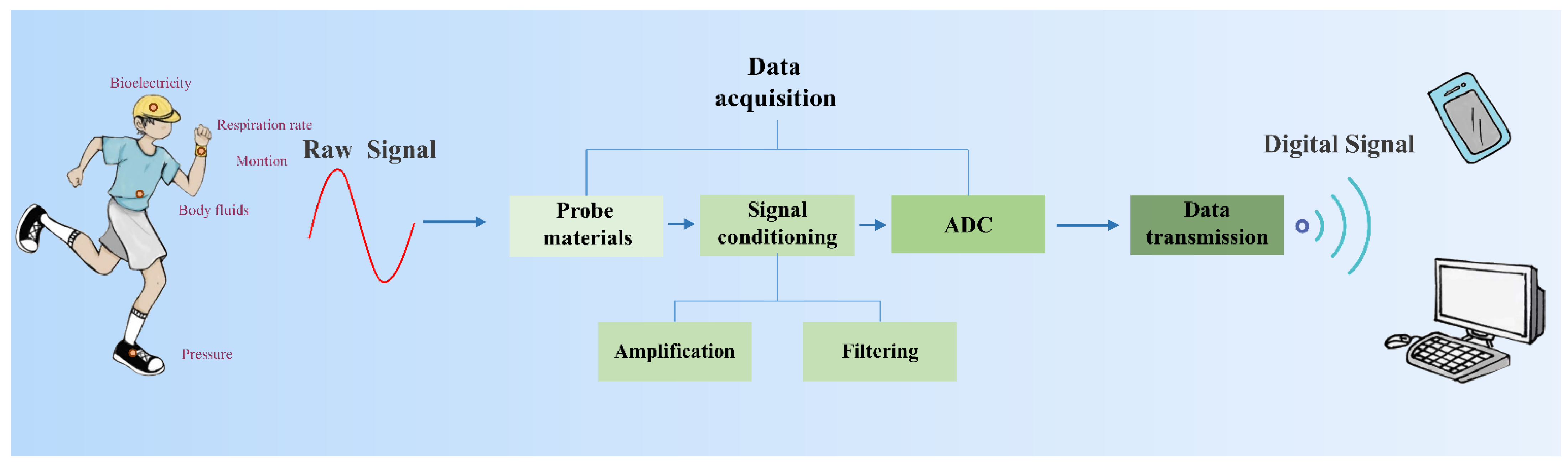
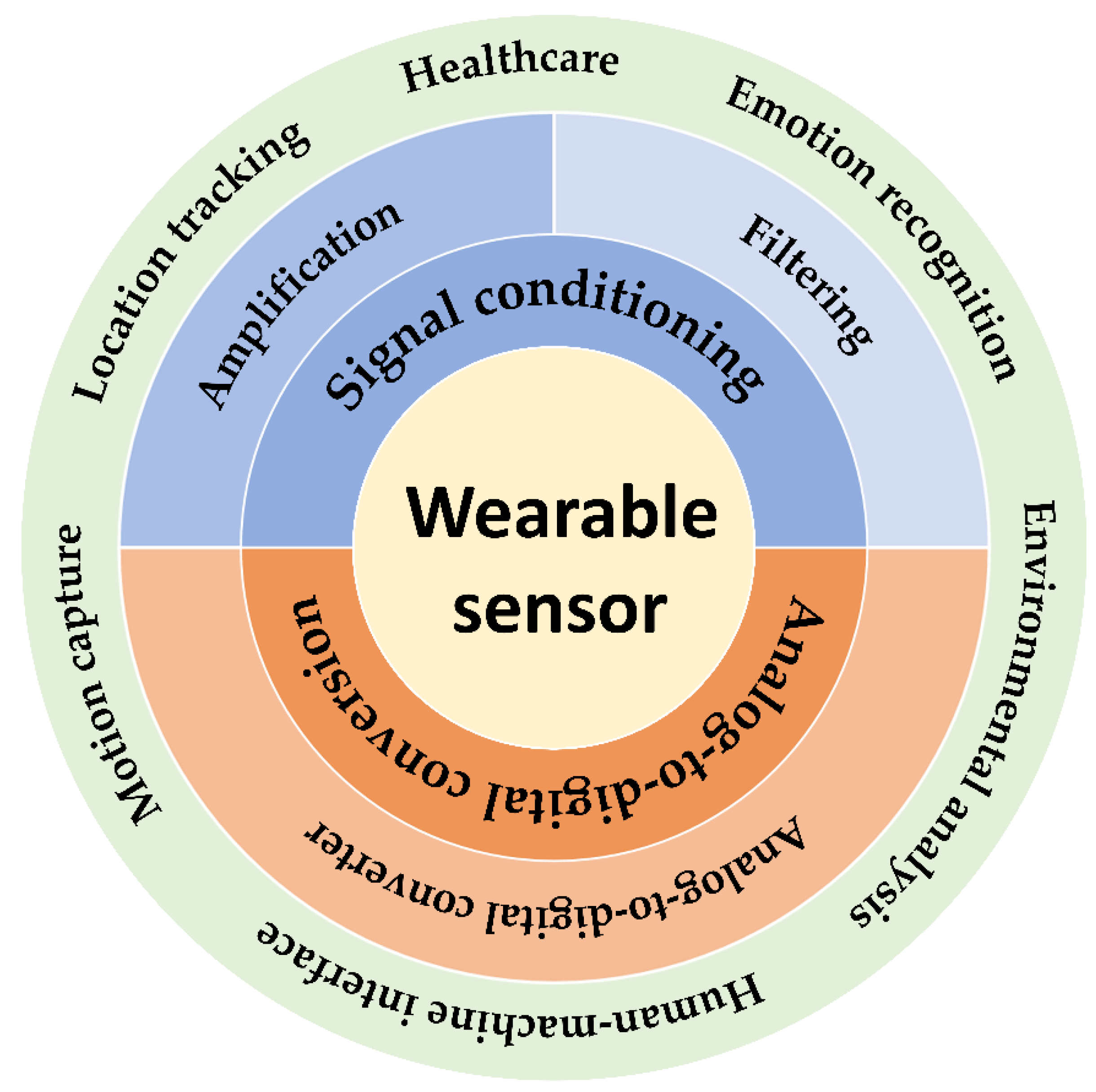
1. Introduction
2. Signal Conditioning
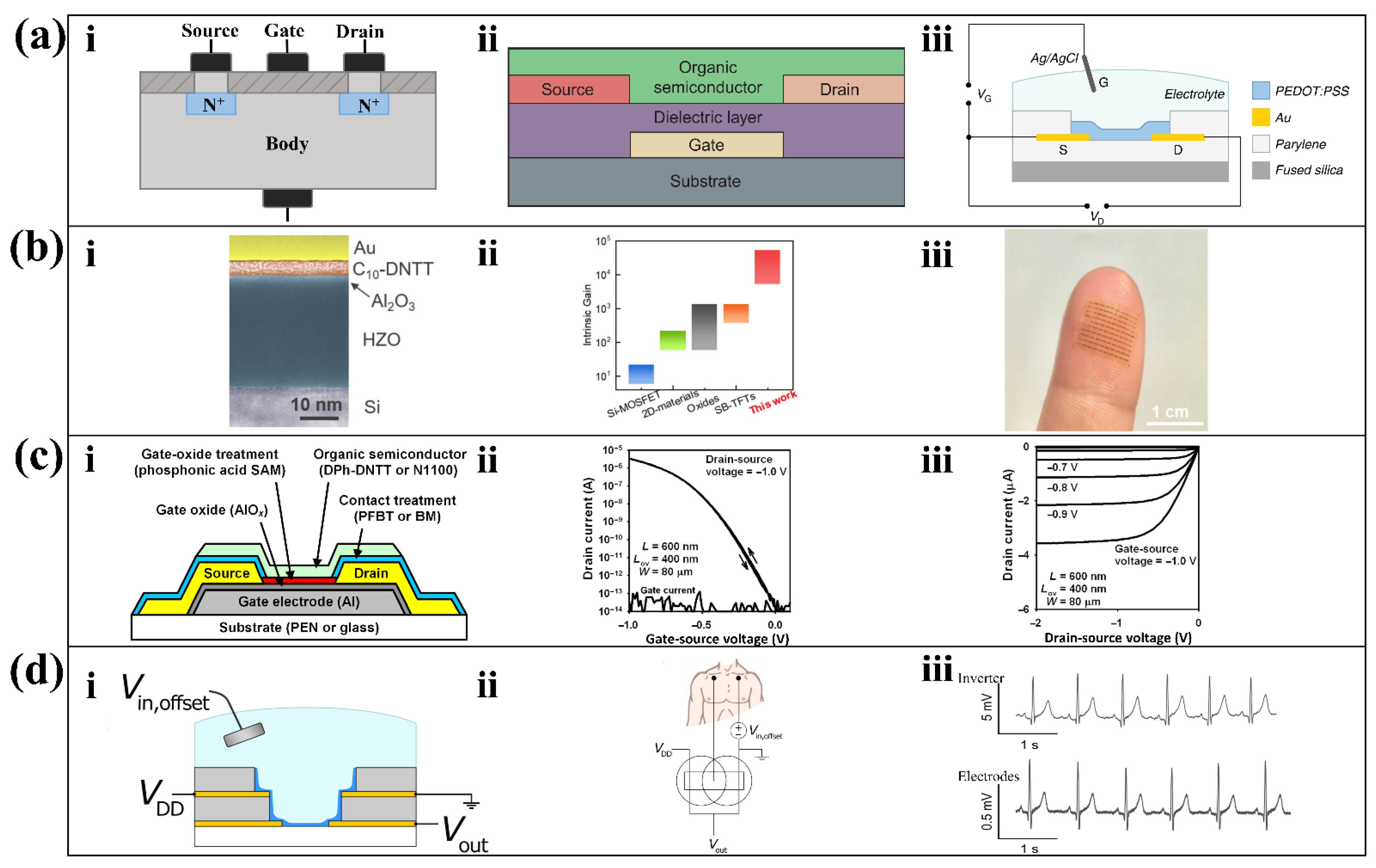
2.1. Amplification
2.1.1. Energy Efficient Design
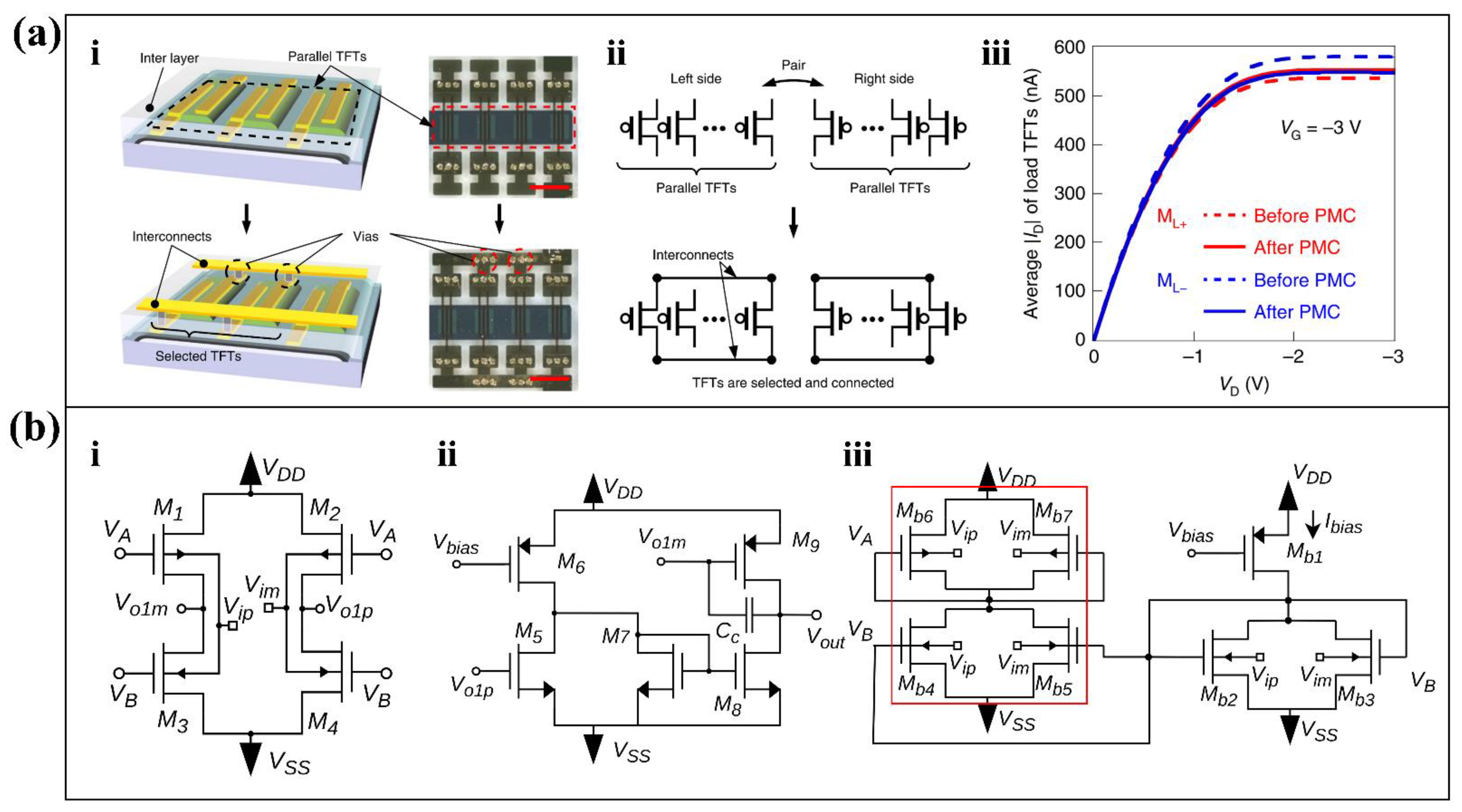
2.1.2. CMRR Enhancements
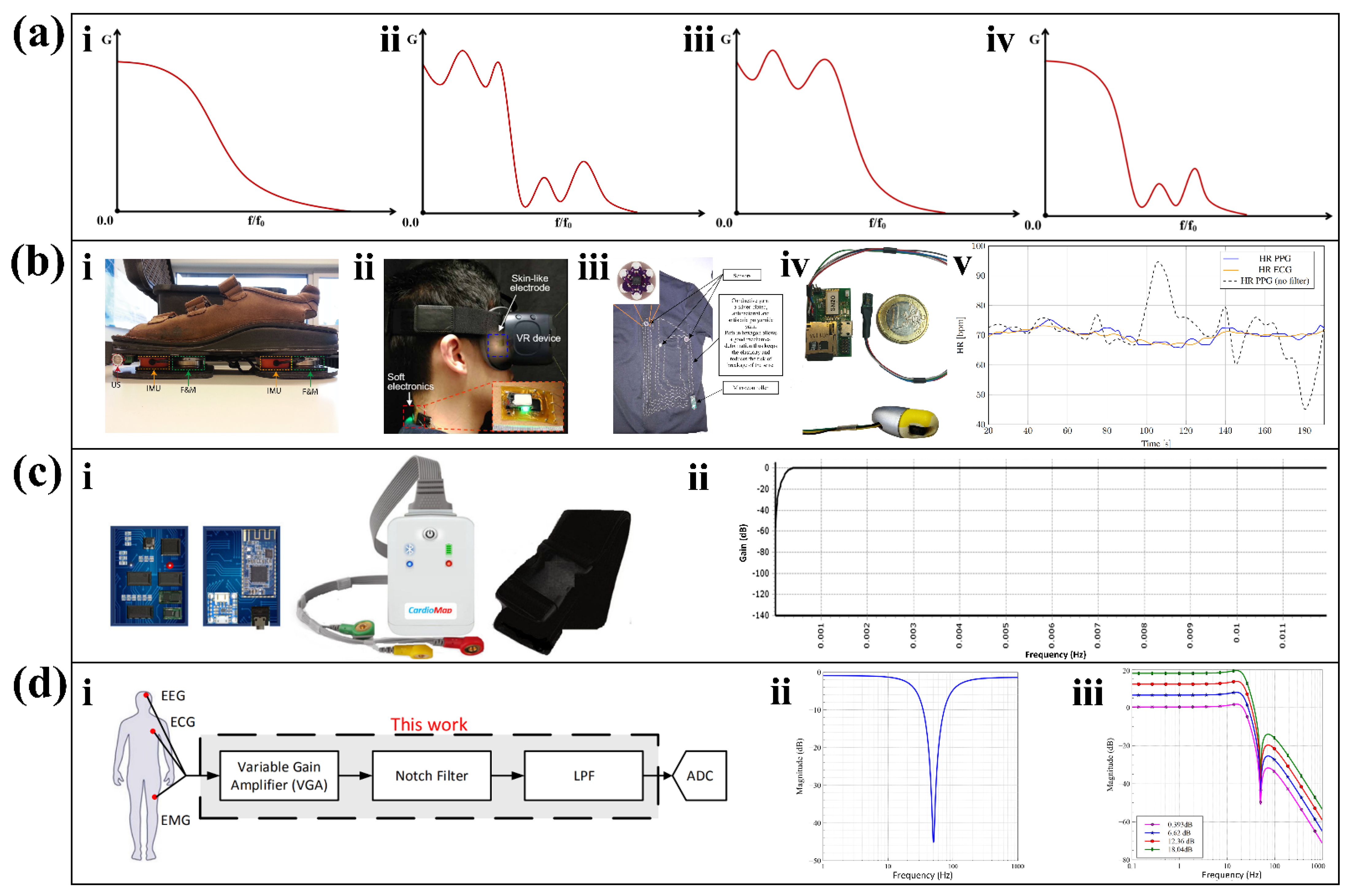
2.2. Filtering
2.2.1. Filter Type
Butterworth Filter
Chebyshev Filter
Elliptic Filter
2.2.2. Applications and Innovation of Filters
3. Analog-to-Digital Conversion
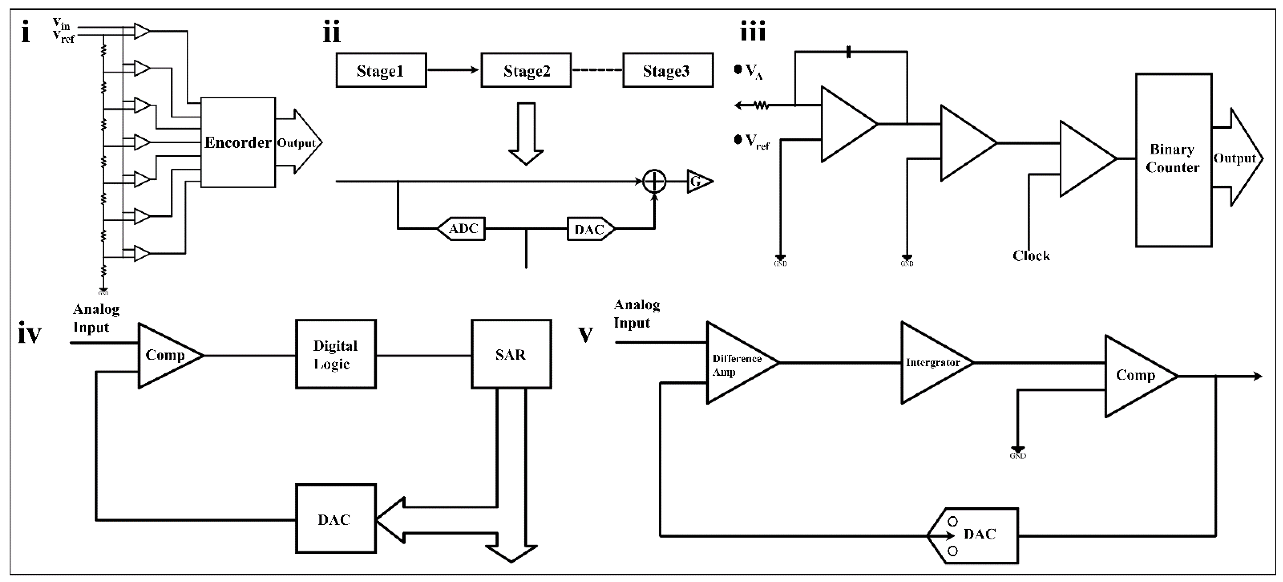
3.1. ADC Types
3.1.1. Flash ADC
3.1.2. Pipeline ADC
3.1.3. Dual Slope ADC
3.1.4. SAR ADC
3.1.5. Sigma-Delta ADC
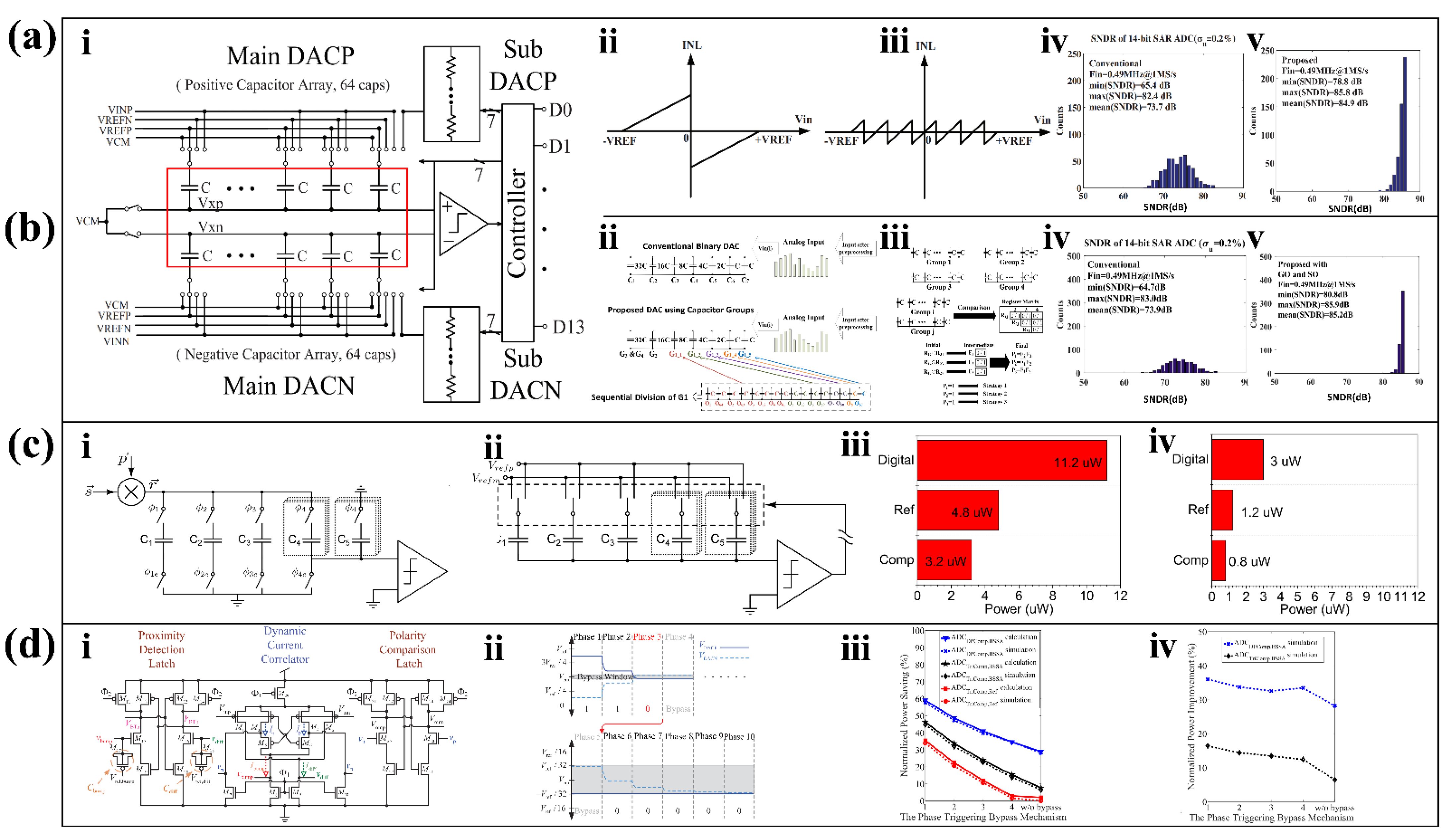
3.2. ADC Optimization Strategy
3.2.1. Linearity Enhancement
3.2.2. Energy Efficient Design
4. Conclusions and Outlook
Author Contributions
Funding
Institutional Review Board Statement
Informed Consent Statement
Data Availability Statement
Conflicts of Interest
Abbreviations
| DAQ | Data acquisition |
| DT | Data transmission |
| ADC | Analog-to-digital convertor |
| CMRR | Common-mode rejection ratio |
| SAR | Successive approximation register |
| FET | Field effect transistor |
| TFT | Thin film transistor |
| OTFT | Organic thin film transistors |
| OECT | Organic electrochemical transistors |
| EEG | Electroencephalogram |
| ECG | Electrocardiogram |
| SAM | Self-assembled monolayer |
| PaC | Parylene C |
| NMOS | Negative metal oxide semiconductor |
| PMOS | Positive metal oxide semiconductor |
| PMC | Post-mismatch compensation |
| CMFF | Common-mode feed-forward |
| TDM | Time division multiplexing |
| AFE ASCI | Analog front-end application specific integrated circuit |
| PPG | Photoplethysmography |
| FDDA | Fully differential difference amplifier |
| OPAMP | Operational amplifier |
| OTA | Operational transconductance amplifier |
| DDA | Differential difference amplifier |
| CMFB | Common mode feedback |
| PSoC | Programmable embedded system-on-chip |
| VGA | Variable gain amplifier |
| SNR | Signal-to-noise ratio |
| CF | Complementary filtering |
| DAC | Digital-to-analog converter |
| SFDR | Spurious-free dynamic range |
| SNDR | Signal-to-noise distortion ratio |
| LSB | Least significant bit |
| CS | Compressive sensing |
| MSB | Most significant bit |
References
- Wang, J.; Zhu, Y.; Wu, Z.; Zhang, Y.; Lin, J.; Chen, T.; Liu, H.; Wang, F.; Sun, L. Wearable multichannel pulse condition monitoring system based on flexible pressure sensor arrays. Microsyst. Nanoeng. 2022, 8, 16. [Google Scholar] [CrossRef]
- Shahrestani, S.; Chou, T.-C.; Shang, K.-M.; Zada, G.; Borok, Z.; Rao, A.P.; Tai, Y.-C. A wearable eddy current based pulmonary function sensor for continuous non-contact point-of-care monitoring during the COVID-19 pandemic. Sci. Rep. 2021, 11, 20144. [Google Scholar] [CrossRef] [PubMed]
- Steinberg, C.; Philippon, F.; Sanchez, M.; Fortier-Poisson, P.; O’Hara, G.; Molin, F.; Sarrazin, J.-F.; Nault, I.; Blier, L.; Roy, K.; et al. A Novel Wearable Device for Continuous Ambulatory ECG Recording: Proof of Concept and Assessment of Signal Quality. Biosensors 2019, 9, 17. [Google Scholar] [CrossRef]
- Wang, L.; Lou, Z.; Jiang, K.; Shen, G. Bio-Multifunctional Smart Wearable Sensors for Medical Devices. Adv. Intell. Syst. 2019, 1, 1900040. [Google Scholar] [CrossRef]
- Moin, A.; Zhou, A.; Rahimi, A.; Menon, A.; Benatti, S.; Alexandrov, G.; Tamakloe, S.; Ting, J.; Yamamoto, N.; Khan, Y.; et al. A wearable biosensing system with in-sensor adaptive machine learning for hand gesture recognition. Nat. Electron. 2021, 4, 54–63. [Google Scholar] [CrossRef]
- Randhawa, P.; Shanthagiri, V.; Kumar, A.; Yadav, V. Human activity detection using machine learning methods from wearable sensors. Sens. Rev. 2020, 40, 591–603. [Google Scholar] [CrossRef]
- Wang, B.; Thukral, A.; Xie, Z.; Liu, L.; Zhang, X.; Huang, W.; Yu, X.; Yu, C.; Marks, T.J.; Facchetti, A. Flexible and stretchable metal oxide nanofiber networks for multimodal and monolithically integrated wearable electronics. Nat. Commun. 2020, 11, 2405. [Google Scholar] [CrossRef]
- Peng, B.; Peng, R.-C.; Zhang, Y.-Q.; Dong, G.; Zhou, Z.; Zhou, Y.; Li, T.; Liu, Z.; Luo, Z.; Wang, S.; et al. Phase transition enhanced superior elasticity in freestanding single-crystalline multiferroic BiFeO3 membranes. Sci. Adv. 2020, 6, eaba5847. [Google Scholar] [CrossRef]
- Lim, Y.W.; Jin, J.; Bae, B.S. Optically Transparent Multiscale Composite Films for Flexible and Wearable Electronics. Adv Mater 2020, 32, e1907143. [Google Scholar] [CrossRef]
- Zhao, X.; Zhou, K.; Zhong, Y.; Liu, P.; Li, Z.; Pan, J.; Long, Y.; Huang, M.; Brakat, A.; Zhu, H. Hydrophobic ionic liquid-in-polymer composites for ultrafast, linear response and highly sensitive humidity sensing. Nano Res. 2021, 14, 1202–1209. [Google Scholar] [CrossRef]
- Wen, J.; Xu, B.; Gao, Y.; Li, M.; Fu, H. Wearable technologies enable high-performance textile supercapacitors with flexible, breathable and wearable characteristics for future energy storage. Energy Stor. Mater. 2021, 37, 94–122. [Google Scholar] [CrossRef]
- He, F.; You, X.; Gong, H.; Yang, Y.; Bai, T.; Wang, W.; Guo, W.; Liu, X.; Ye, M. Stretchable, Biocompatible, and Multifunctional Silk Fibroin-Based Hydrogels toward Wearable Strain/Pressure Sensors and Triboelectric Nanogenerators. ACS Appl Mater Interfaces 2020, 12, 6442–6450. [Google Scholar] [CrossRef]
- Lim, C.; Shin, Y.; Jung, J.; Kim, j.h.; Lee, S.; Kim, D.-H. Stretchable conductive nanocomposite based on alginate hydrogel and silver nanowires for wearable electronics. APL Mater. 2019, 7, 031502. [Google Scholar] [CrossRef]
- Ohm, Y.; Pan, C.; Ford, M.J.; Huang, X.; Liao, J.; Majidi, C. An electrically conductive silver–polyacrylamide–alginate hydrogel composite for soft electronics. Nat. Electron. 2021, 4, 185–192. [Google Scholar] [CrossRef]
- Zhao, X.; Zhou, Y.; Xu, J.; Chen, G.; Fang, Y.; Tat, T.; Xiao, X.; Song, Y.; Li, S.; Chen, J. Soft fibers with magnetoelasticity for wearable electronics. Nat. Commun. 2021, 12, 6755. [Google Scholar] [CrossRef] [PubMed]
- Lv, J.; Thangavel, G.; Li, Y.; Xiong, J.; Gao, D.; Ciou, J.; Tan, M.W.M.; Aziz, I.; Chen, S.; Chen, J.; et al. Printable elastomeric electrodes with sweat-enhanced conductivity for wearables. Sci. Adv. 2021, 7, eabg8433. [Google Scholar] [CrossRef] [PubMed]
- Wang, B.; Shi, T.; Zhang, Y.; Chen, C.; Li, Q.; Fan, Y. Lignin-based highly sensitive flexible pressure sensor for wearable electronics. J. Mater. Chem. C 2018, 6, 6423–6428. [Google Scholar] [CrossRef]
- Li, X.; Fan, Y.J.; Li, H.Y.; Cao, J.W.; Xiao, Y.C.; Wang, Y.; Liang, F.; Wang, H.L.; Jiang, Y.; Wang, Z.L.; et al. Ultracomfortable Hierarchical Nanonetwork for Highly Sensitive Pressure Sensor. ACS Nano 2020, 14, 9605–9612. [Google Scholar] [CrossRef]
- Wang, R.; Zhai, Q.; An, T.; Gong, S.; Cheng, W. Stretchable gold fiber-based wearable textile electrochemical biosensor for lactate monitoring in sweat. Talanta 2021, 222, 121484. [Google Scholar] [CrossRef] [PubMed]
- Liu, H.; Wang, L.; Lin, G.; Feng, Y. Recent progress in the fabrication of flexible materials for wearable sensors. Biomaterials Science 2022, 10, 614–632. [Google Scholar] [CrossRef]
- Gao, W.; Ota, H.; Kiriya, D.; Takei, K.; Javey, A. Flexible Electronics toward Wearable Sensing. Acc. Chem. Res. 2019, 52, 523–533. [Google Scholar] [CrossRef]
- Lim, H.-R.; Kim, H.S.; Qazi, R.; Kwon, Y.-T.; Jeong, J.-W.; Yeo, W.-H. Advanced Soft Materials, Sensor Integrations, and Applications of Wearable Flexible Hybrid Electronics in Healthcare, Energy, and Environment. Adv. Mater. 2020, 32, 1901924. [Google Scholar] [CrossRef]
- Heikenfeld, J.; Jajack, A.; Rogers, J.; Gutruf, P.; Tian, L.; Pan, T.; Li, R.; Khine, M.; Kim, J.; Wang, J.; et al. Wearable sensors: Modalities, challenges, and prospects. Lab Chip 2018, 18, 217–248. [Google Scholar] [CrossRef] [PubMed]
- Celka, P.; Vetter, R.; Renevey, P.; Verjus, C.; Neuman, V.; Luprano, J.; Decotignie, J.-D.; Piguet, C. Wearable biosensing: Signal processing and communication architectures issues. J. Telecommun. Inf. Technol. 2004, 4, 90–104. [Google Scholar]
- Wadhera, T.; Kakkar, D.; Wadhwa, G.; Raj, B. Recent Advances and Progress in Development of the Field Effect Transistor Biosensor: A Review. J. Electron. Mater. 2019, 48, 7635–7646. [Google Scholar] [CrossRef]
- Zang, Y.; Zhang, F.; Huang, D.; Gao, X.; Di, C.-A.; Zhu, D. Flexible suspended gate organic thin-film transistors for ultra-sensitive pressure detection. Nat. Commun. 2015, 6, 6269. [Google Scholar] [CrossRef]
- Minamiki, T.; Minami, T.; Chen, Y.-P.; Mano, T.; Takeda, Y.; Fukuda, K.; Tokito, S. Flexible organic thin-film transistor immunosensor printed on a one-micron-thick film. Commun. Mater 2021, 2, 8. [Google Scholar] [CrossRef]
- Rivnay, J.; Inal, S.; Salleo, A.; Owens, R.M.; Berggren, M.; Malliaras, G.G. Organic electrochemical transistors. Nat. Rev. Mater. 2018, 3, 17086. [Google Scholar] [CrossRef]
- Hai, W.; Goda, T.; Takeuchi, H.; Yamaoka, S.; Horiguchi, Y.; Matsumoto, A.; Miyahara, Y. Human influenza virus detection using sialyllactose-functionalized organic electrochemical transistors. Sens. Actuators B Chem. 2018, 260, 635–641. [Google Scholar] [CrossRef]
- Bihar, E.; Deng, Y.; Miyake, T.; Saadaoui, M.; Malliaras, G.G.; Rolandi, M. A Disposable paper breathalyzer with an alcohol sensing organic electrochemical transistor. Sci. Rep. 2016, 6, 27582. [Google Scholar] [CrossRef]
- Mahmood, M.; Mzurikwao, D.; Kim, Y.-S.; Lee, Y.; Mishra, S.; Herbert, R.; Duarte, A.; Ang, C.S.; Yeo, W.-H. Fully portable and wireless universal brain–machine interfaces enabled by flexible scalp electronics and deep learning algorithm. Nat. Mach. Intell 2019, 1, 412–422. [Google Scholar] [CrossRef]
- Zulqarnain, M.; Stanzione, S.; Rathinavel, G.; Smout, S.; Willegems, M.; Myny, K.; Cantatore, E. A flexible ECG patch compatible with NFC RF communication. NPJ Flex. Electron. 2020, 4, 13. [Google Scholar] [CrossRef]
- Ershad, F.; Thukral, A.; Yue, J.; Comeaux, P.; Lu, Y.; Shim, H.; Sim, K.; Kim, N.-I.; Rao, Z.; Guevara, R.; et al. Ultra-conformal drawn-on-skin electronics for multifunctional motion artifact-free sensing and point-of-care treatment. Nat. Commun. 2020, 11, 3823. [Google Scholar] [CrossRef] [PubMed]
- Reese, C.; Roberts, M.; Ling, M.-M.; Bao, Z. Organic thin film transistors. Mater. Today 2004, 7, 20–27. [Google Scholar] [CrossRef]
- Khodagholy, D.; Rivnay, J.; Sessolo, M.; Gurfinkel, M.; Leleux, P.; Jimison, L.H.; Stavrinidou, E.; Herve, T.; Sanaur, S.; Owens, R.M.; et al. High transconductance organic electrochemical transistors. Nat. Commun. 2013, 4, 2133. [Google Scholar] [CrossRef]
- Luo, Z.; Peng, B.; Zeng, J.; Yu, Z.; Zhao, Y.; Xie, J.; Lan, R.; Ma, Z.; Pan, L.; Cao, K.; et al. Sub-thermionic, ultra-high-gain organic transistors and circuits. Nat. Commun. 2021, 12, 1928. [Google Scholar] [CrossRef]
- Zschieschang, U.; Waizmann, U.; Weis, J.; Borchert James, W.; Klauk, H. Nanoscale flexible organic thin-film transistors. Sci. Adv. 2022, 8, eabm9845. [Google Scholar] [CrossRef]
- Rashid Reem, B.; Du, W.; Griggs, S.; Maria Iuliana, P.; McCulloch, I.; Rivnay, J. Ambipolar inverters based on cofacial vertical organic electrochemical transistor pairs for biosignal amplification. Sci. Adv. 2021, 7, eabh1055. [Google Scholar] [CrossRef]
- Abarkan, M.; Pirog, A.; Mafilaza, D.; Pathak, G.; N'Kaoua, G.; Puginier, E.; O'Connor, R.; Raoux, M.; Donahue, M.J.; Renaud, S.; et al. Vertical Organic Electrochemical Transistors and Electronics for Low Amplitude Micro-Organ Signals. Sci. Adv. 2022, 9, 2105211. [Google Scholar] [CrossRef] [PubMed]
- Karami Horestani, F.; Eshghi, M.; Yazdchi, M. An ultra-low power amplifier for wearable and implantable electronic devices. Microelectron. Eng. 2019, 216, 111054. [Google Scholar] [CrossRef]
- Zhou, Z.; Zhu, L.; Yang, R.; Li, J.; Wang, W.; Pan, J.; Liu, M.; Wang, K.; Wang, Z. A High CMRR Instrumentation Amplifier Employing Pseudo-Differential Inverter for Neural Signal Sensing. IEEE Sens. J. 2022, 22, 419–427. [Google Scholar] [CrossRef]
- Xu, J.; Mitra, S.; Hoof, C.V.; Yazicioglu, R.F.; Makinwa, K.A.A. Active Electrodes for Wearable EEG Acquisition: Review and Electronics Design Methodology. IEEE Rev. Biomed. Eng 2017, 10, 187–198. [Google Scholar] [CrossRef] [PubMed]
- Fuketa, H.; Yoshioka, K.; Shinozuka, Y.; Ishida, K.; Yokota, T.; Matsuhisa, N.; Inoue, Y.; Sekino, M.; Sekitani, T.; Takamiya, M.; et al. 1 μm-thickness ultra-flexible and high electrode-density surface electromyogram measurement sheet with 2 V organic transistors for prosthetic hand control. IEEE Trans. Biomed. Circuits Syst. 2014, 8, 824–833. [Google Scholar] [CrossRef]
- Centurelli, F.; Della Sala, R.; Scotti, G.; Trifiletti, A. A 0.3 V, Rail-to-Rail, Ultralow-Power, Non-Tailed, Body-Driven, Sub-Threshold Amplifier. Appl. Sci. 2021, 11, 2528. [Google Scholar] [CrossRef]
- Tang, T.; Goh, W.L.; Yao, L.; Gao, Y. A TDM-Based 16-Channel AFE ASIC With Enhanced System-Level CMRR for Wearable EEG Recording With Dry Electrodes. IEEE Trans. Biomed. Circuits Syst. 2020, 14, 516–524. [Google Scholar] [CrossRef]
- Kim, J. Simultaneous Voltage and Current Measurement Instrumentation Amplifier for ECG and PPG Monitoring. Electronics 2021, 10, 679. [Google Scholar] [CrossRef]
- Chen, C.; Ma, Z.; Liu, Z.; Zhou, L.; Wang, G.; Li, Y.; Zhao, J. An Energy-Efficient Wearable Functional Near-infrared Spectroscopy System Employing Dual-level Adaptive Sampling Technique. IEEE Trans. Biomed. Circuits Syst. 2022, 16, 119–128. [Google Scholar] [CrossRef]
- Enz, C.C.; Temes, G.C. Circuit techniques for reducing the effects of op-amp imperfections: Autozeroing, correlated double sampling, and chopper stabilization. Proc. IEEE Inst. Electr. Electron. Eng. 1996, 84, 1584–1614. [Google Scholar] [CrossRef]
- Agnes, A.; Cabrini, A.; Maloberti, F.; Martini, G. Cancellation of Amplifier Offset and 1/f Noise: An Improved Chopper Stabilized Technique. IEEE Trans. Circuits Syst. II 2007, 54, 469–473. [Google Scholar] [CrossRef]
- Zhao, Y.; Shang, Z.; Lian, Y. A 2.55 NEF 76 dB CMRR DC-Coupled Fully Differential Difference Amplifier Based Analog Front End for Wearable Biomedical Sensors. IEEE Trans. Biomed. Circuits Syst. 2019, 13, 918–926. [Google Scholar] [CrossRef]
- Harrison, R.R.; Watkins, P.T.; Kier, R.J.; Lovejoy, R.O.; Black, D.J.; Greger, B.; Solzbacher, F. A Low-Power Integrated Circuit for a Wireless 100-Electrode Neural Recording System. IEEE J. Solid-State Circuits 2007, 42, 123–133. [Google Scholar] [CrossRef]
- Borchert, J.W.; Zschieschang, U.; Letzkus, F.; Giorgio, M.; Weitz, R.T.; Caironi, M.; Burghartz, J.N.; Ludwigs, S.; Klauk, H. Flexible low-voltage high-frequency organic thin-film transistors. Sci. Adv. 2020, 6, eaaz5156. [Google Scholar] [CrossRef]
- Rashid, R.B.; Ciechowski, R.J.; Rivnay, J. Self-aligned, laser-cut organic electrochemical transistors. Flex. Print. Electron 2020, 5, 014007. [Google Scholar] [CrossRef]
- Holleman, J.; Otis, B. A Sub-Microwatt Low-Noise Amplifier for Neural Recording. In Proceedings of the 2007 29th Annual International Conference of the IEEE Engineering in Medicine and Biology Society, Lyon, France, 22–26 August 2007; pp. 3930–3933. [Google Scholar] [CrossRef]
- Yang, T.; Lu, J.; Poore, N.; Holleman, J. A current-reuse complementary-input chopper-stabilized amplifier for neural recording. In Proceedings of the 2014 IEEE 12th International New Circuits and Systems Conference (NEWCAS), Trois-Rivieres, QC, Canada, 22–25 June 2014; pp. 85–88. [Google Scholar]
- Zhang, F.; Holleman, J.; Otis, B.P. Design of ultra-low power biopotential amplifiers for biosignal acquisition applications. IEEE Trans. Biomed. Circuits Syst. 2012, 6, 344–355. [Google Scholar] [CrossRef]
- Tasneem, N.T.; Biswas, D.K.; Adhikari, P.R.; Reid, R.; Mahbub, I. Design of a Reverse-Electrowetting Transducer Based Wireless Self-Powered Motion Sensor. In Proceedings of the 2020 IEEE International Symposium on Circuits and Systems (ISCAS), Seville, Spain, 12–14 202 October 2020; pp. 1–5. [Google Scholar]
- Sugiyama, M.; Uemura, T.; Kondo, M.; Akiyama, M.; Namba, N.; Yoshimoto, S.; Noda, Y.; Araki, T.; Sekitani, T. An ultraflexible organic differential amplifier for recording electrocardiograms. Nat. Electron. 2019, 2, 351–360. [Google Scholar] [CrossRef]
- Liu, L.; Gao, D.; Tian, Y.; Yu, Y.; Qin, Z. A Low Mismatch and High Input Impedance Multi-Channel Time-Division Multiplexing Analog Front End for Bio-Sensors. IEEE Sens. J. 2022, 22, 6755–6763. [Google Scholar] [CrossRef]
- Silverio, A.A. Design of a Wide Temperature Range, High Linearity Time Domain CMOS-Based Temperature Sensor for Wearable IOT Applications. In Proceedings of the 2021 2nd International Conference on Innovative and Creative Information Technology (ICITech), Salatiga, Indonesia, 23–25 September 2021; pp. 226–230. [Google Scholar]
- Sawigun, C.; Thanapitak, S. A Compact Sub-μW CMOS ECG Amplifier with 57.5-MΩ Z(in), 2.02 NEF, 8.16 PEF and 83.24-dB CMRR. IEEE Trans. Biomed. Circuits Syst. 2021, 15, 549–558. [Google Scholar] [CrossRef] [PubMed]
- Dementyev, A.; Smith, J. A Wearable UHF RFID-Based EEG System. In Proceedings of the 2013 IEEE International Conference on RFID (RFID), Orlando, FL, USA, 30 April–2 May 2013; pp. 1–7. [Google Scholar]
- De Luca, C.J.; Gilmore, L.D.; Kuznetsov, M.; Roy, S.H. Filtering the surface EMG signal: Movement artifact and baseline noise contamination. J. Biomech. 2010, 43, 1573–1579. [Google Scholar] [CrossRef]
- Ifeachor, E.C.; Jervis, B.W.; Dagless, E.L.; O’Reilly, J. Digital Signal Processing: A Practical Approach; Prentice Hall: Hoboken, NJ, USA, 1993. [Google Scholar]
- Rehman, A.; Mustafa, M.; Javaid, N.; Qasim, U.; Khan, Z.A. Analytical Survey of Wearable Sensors. In Proceedings of the 2012 Seventh International Conference on Broadband, Wireless Computing, Communication and Applications, Victoria, BC, Canada, 12–14 November 2012; pp. 408–413. [Google Scholar]
- Mohamed Refai, M.I.; van Beijnum, B.F.; Buurke, J.H.; Veltink, P.H. Gait and Dynamic Balance Sensing Using Wearable Foot Sensors. IEEE Trans Neural Syst Rehabil Eng 2019, 27, 218–227. [Google Scholar] [CrossRef]
- Mishra, S.; Kim, Y.S.; Intarasirisawat, J.; Kwon, Y.T.; Lee, Y.; Mahmood, M.; Lim, H.R.; Herbert, R.; Yu, K.J.; Ang, C.S.; et al. Soft, wireless periocular wearable electronics for real-time detection of eye vergence in a virtual reality toward mobile eye therapies. Sci Adv 2020, 6, eaay1729. [Google Scholar] [CrossRef]
- Tartare, G.; Zeng, X.; Koehl, L. Development of a wearable system for monitoring the firefighter's physiological state. In Proceedings of the 2018 IEEE Industrial Cyber-Physical Systems (ICPS), St. Petersburg, Russia, 15–18 May 2018; pp. 561–566. [Google Scholar]
- Pedrana, A.; Comotti, D.; Re, V.; Traversi, G. Development of a Wearable In-Ear PPG System for Continuous Monitoring. IEEE Sens. J. 2020, 20, 14482–14490. [Google Scholar] [CrossRef]
- Ali, H.; Naing, H.H.; Yaqub, R. An IoT Assisted Real-Time High CMRR Wireless Ambulatory ECG Monitoring System with Arrhythmia Detection. Electron. 2021, 10, 1871. [Google Scholar] [CrossRef]
- Diab, M.S.; Mahmoud, S.A. 14:5nW; 30 dB Analog Front-End in 90-nm Technology for Biopotential Signal Detection. In Proceedings of the 2020 43rd International Conference on Telecommunications and Signal Processing (TSP), Milan, Italy, 7–9 July 2020; pp. 681–684. [Google Scholar]
- Kim, J.K.; Ahn, J.M. Design of an optimal digital IIR filter for heart rate variability by photoplethysmogram. Int. J. Eng. Res. 2018, 11, 2009–2021. [Google Scholar]
- Huang, H.Y.; Chen, K.Y.; Xie, J.H.; Lee, M.T.; Hong, H.C.; Cheng, K.H. Gm-C filter with automatic calibration scheme. In Proceedings of the 2016 IEEE 19th International Symposium on Design and Diagnostics of Electronic Circuits & Systems (DDECS), Kosice, Slovakia, 20–22 April 2016; pp. 1–4. [Google Scholar]
- Papi, E.; Koh, W.S.; McGregor, A.H. Wearable technology for spine movement assessment: A systematic review. J. Biomech. 2017, 64, 186–197. [Google Scholar] [CrossRef]
- Sprager, S.; Juric, M.B. Inertial Sensor-Based Gait Recognition: A Review. Sensors 2015, 15, 22089–22127. [Google Scholar] [CrossRef]
- Antar, A.D.; Ahmed, M.; Ahad, M.A.R. Challenges in Sensor-based Human Activity Recognition and a Comparative Analysis of Benchmark Datasets: A Review. In Proceedings of the 2019 Joint 8th International Conference on Informatics, Electronics & Vision (ICIEV) and 2019 3rd International Conference on Imaging, Vision & Pattern Recognition (icIVPR), Spokane, WA, USA, 30 May–2 June 2019; pp. 134–139. [Google Scholar]
- Sardini, E.; Serpelloni, M. Instrumented wearable belt for wireless health monitoring. Procedia Eng. 2010, 5, 580–583. [Google Scholar] [CrossRef]
- Roland, T.; Amsuess, S.; Russold, M.F.; Baumgartner, W. Ultra-Low-Power Digital Filtering for Insulated EMG Sensing. Sensors 2019, 19, 959. [Google Scholar] [CrossRef]
- Liang, Y.; Elgendi, M.; Chen, Z.; Ward, R. An optimal filter for short photoplethysmogram signals. Sci. Data 2018, 5, 180076. [Google Scholar] [CrossRef]
- Silverio, A.A.; Asilo, J.E.; Balagat, S.L.D.; Pineda, A.A.; Tangi, J.A.; Tuazon, D.T.P.; Piedra, B.M.B. Micromotion Artefact Reduction of a Wrist Worn PPG Sensor Using Green Light PPG and Surface EMG. In Proceedings of the 2020 IEEE 8th R10 Humanitarian Technology Conference (R10-HTC), Kuching, Malaysia, 1–3 December 2020; pp. 1–5. [Google Scholar]
- Bastos, L.; Tavares, T.; Rosário, D.; Cerqueira, E.; Santos, A.; Nogueira, M. Double Authentication Model based on PPG and ECG Signals. In Proceedings of the 2020 International Wireless Communications and Mobile Computing (IWCMC), Limassol, Cyprus, 15–19 June 2020; pp. 601–606. [Google Scholar]
- Prashar, N.; Dogra, J.; Sood, M.; Jain, S. Removal of electromyography noise from ECG for high performance biomedical systems. Netw. Biol. 2018, 8, 12–24. [Google Scholar]
- Fletcher, R.R.; Tam, S.; Omojola, O.; Redemske, R.; Kwan, J. Wearable sensor platform and mobile application for use in cognitive behavioral therapy for drug addiction and PTSD. In Proceedings of the 2011 Annual International Conference of the IEEE Engineering in Medicine and Biology Society, Boston, MA, USA, 30 August–3 September 2011; pp. 1802–1805. [Google Scholar]
- Majoe, D.; Bonhof, P.; Kaegi-Trachsel, T.; Gutknecht, J.; Widmer, L. Stress and sleep quality estimation from a smart wearable sensor. In Proceedings of the 5th International Conference on Pervasive Computing and Applications, Hualien, Taiwan, 1–3 December 2010; pp. 14–19. [Google Scholar]
- Jamal, M.Z.; Lee, D.; Hyun, D.J. Real Time Adaptive Filter based EMG Signal Processing and Instrumentation Scheme for Robust Signal Acquisition Using Dry EMG Electrodes. In Proceedings of the 2019 16th International Conference on Ubiquitous Robots (UR), Jeju, Korea, 24–27 June 2019; pp. 683–688. [Google Scholar]
- Gustafsson, F.; Gunnarsson, F.; Bergman, N.; Forssell, U.; Jansson, J.; Karlsson, R.; Nordlund, P.J. Particle filters for positioning, navigation, and tracking. IEEE Trans. Signal Process. 2002, 50, 425–437. [Google Scholar] [CrossRef]
- Zizzo, G.; Ren, L. Position Tracking During Human Walking Using an Integrated Wearable Sensing System. Sensors 2017, 17, 2866. [Google Scholar] [CrossRef] [PubMed]
- Poulose, A.; Senouci, B.; Han, D.S. Performance Analysis of Sensor Fusion Techniques for Heading Estimation Using Smartphone Sensors. IEEE Sens. J. 2019, 19, 12369–12380. [Google Scholar] [CrossRef]
- El-Gohary, M.; McNames, J. Human Joint Angle Estimation with Inertial Sensors and Validation with A Robot Arm. IEEE. Trans. Biomed. Eng. 2015, 62, 1759–1767. [Google Scholar] [CrossRef]
- Elgendi, M.; Fletcher, R.; Liang, Y.; Howard, N.; Lovell, N.H.; Abbott, D.; Lim, K.; Ward, R. The use of photoplethysmography for assessing hypertension. NPJ Digit. Med. 2019, 2, 60. [Google Scholar] [CrossRef] [PubMed]
- Elgendi, M. On the analysis of fingertip photoplethysmogram signals. Curr. Cardiol. Rev. 2012, 8, 14–25. [Google Scholar] [CrossRef] [PubMed]
- Carpenter, J.; Clifford, P.; Fearnhead, P. Improved particle filter for nonlinear problems. IEE Proceedings-Radar, Sonar and Navigation 1999, 146, 2–7. [Google Scholar] [CrossRef]
- Sasiadek, J.Z. Sensor fusion. Annu. Rev. Control 2002, 26, 203–228. [Google Scholar] [CrossRef]
- Xia, K.; Wang, H.; Xu, M.; Li, Z.; He, S.; Tang, Y. Racquet Sports Recognition Using a Hybrid Clustering Model Learned from Integrated Wearable Sensor. Sensors 2020, 20, 1638. [Google Scholar] [CrossRef]
- Gui, P.; Tang, L.; Mukhopadhyay, S. MEMS based IMU for tilting measurement: Comparison of complementary and kalman filter based data fusion. In Proceedings of the 2015 IEEE 10th Conference on Industrial Electronics and Applications (ICIEA), Auckland, New Zealand, 15–17 June 2015; pp. 2004–2009. [Google Scholar]
- Bashir, S.; Ali, S.; Ahmed, S.; Kakkar, V. Analog-to-digital converters: A comparative study and performance analysis. In Proceedings of the 2016 International Conference on Computing, Communication and Automation (ICCCA), Noida, India, 29–30 April 2016; pp. 999–1001. [Google Scholar]
- Hussain, T.; Zakir, G.; Sheikh, M.R.I. State-of-the-art pipeline A/D converter survey and analysis. In Proceedings of the 2012 International Conference on Informatics, Electronics & Vision (ICIEV), Dhaka, Bangladesh, 18–19 May 2012; pp. 476–481. [Google Scholar]
- Sonkusale, S.; Van der Spiegel, J.; Nagaraj, K. True background calibration technique for pipelined ADC. Electron. Lett. 2000, 36, 786–788. [Google Scholar] [CrossRef]
- Taha, S.M.R. Speed Improvements for Dual-Slope A/D Converters. IEEE Trans. Instrum. Meas. 1985, IM-34, 630–635. [Google Scholar] [CrossRef]
- Krad, H. A dual-slope integration based analog-to-digital convertor. Am. J. Appl. Sci. 2009, 2, 743–749. [Google Scholar] [CrossRef]
- Lin, Q.; Xu, J.; Song, S.; Breeschoten, A.; Konijnenburg, M.; Chen, M.; Hoof, C.V.; Tavernier, F.; Helleputte, N.V. A 196μW, Reconfigurable Light-to-Digital Converter with 119dB Dynamic Range, for Wearable PPG/NIRS Sensors. In Proceedings of the 2019 Symposium on VLSI Circuits, Kyoto, Japan, 9–14 June 2019; pp. C58–C59. [Google Scholar]
- O’Driscoll, S.; Shenoy, K.; Meng, T. Adaptive Resolution ADC Array for an Implantable Neural Sensor. Biomed. Circuits Syst. IEEE Trans. 2011, 5, 120–130. [Google Scholar] [CrossRef] [PubMed][Green Version]
- Lin, B.; Ma, Z.; Atef, M.; Ying, L.; Wang, G. Low-Power High-Sensitivity Photoplethysmography Sensor for Wearable Health Monitoring System. IEEE Sens. J. 2021, 21, 16141–16151. [Google Scholar] [CrossRef]
- Milosevic, B.; Farella, E.; Benatti, S. Exploring Arm Posture and Temporal Variability in Myoelectric Hand Gesture Recognition. In Proceedings of the 2018 7th IEEE International Conference on Biomedical Robotics and Biomechatronics (Biorob), Enschede, The Netherlands, 26–29 August 2018; pp. 1032–1037. [Google Scholar]
- An, S.; Xia, S.; Ma, Y.; Ghani, A.; See, C.H.; Abd-Alhameed, R.A.; Niu, C.; Yang, R. A Low Power Sigma-Delta Modulator with Hybrid Architecture. Sensors 2020, 20, 5309. [Google Scholar] [CrossRef]
- Lopez-Morillo, E.; Carvajal, R.G.; Munoz, F.; Gmili, H.E.; Lopez-Martin, A.; Ramirez-Angulo, J.; Rodriguez-Villegas, E. A 1.2-V 140-nW 10-bit Sigma–Delta Modulator for Electroencephalogram Applications. IEEE Trans. Biomed. Circuits Syst. 2008, 2, 223–230. [Google Scholar] [CrossRef]
- Teague, C.N.; Heller, J.A.; Nevius, B.N.; Carek, A.M.; Mabrouk, S.; Garcia-Vicente, F.; Inan, O.T.; Etemadi, M. A Wearable, Multimodal Sensing System to Monitor Knee Joint Health. IEEE Sens. J. 2020, 20, 10323–10334. [Google Scholar] [CrossRef]
- Kim, J.; Yoo, T.; Baek, K.-H.; Kim, T.T.-H. Balanced sampling switch for high linearity and a wide temperature range in low power SAR ADCs. Electron. Lett. 2019, 55, 1273–1275. [Google Scholar] [CrossRef]
- Miki, T.; Morie, T.; Matsukawa, K.; Bando, Y.; Okumoto, T.; Obata, K.; Sakiyama, S.; Dosho, S. A 4.2 mW 50 MS/s 13 bit CMOS SAR ADC With SNR and SFDR Enhancement Techniques. IEEE J. Solid-State Circuits 2015, 50, 1372–1381. [Google Scholar] [CrossRef]
- Fan, H.; Heidari, H.; Maloberti, F.; Li, D.; Hu, D.; Cen, Y. High resolution and linearity enhanced SAR ADC for wearable sensing systems. In Proceedings of the 2017 IEEE International Symposium on Circuits and Systems (ISCAS), Baltimore, MD, USA, 28–31 May 2017; pp. 1–4. [Google Scholar]
- Fan, H.; Li, J.; Feng, Q.; Diao, X.; Lin, L.; Zhang, K.; Sun, H.; Heidari, H. Exploiting Smallest Error to Calibrate Non-Linearity in SAR Adcs. IEEE Access 2018, 6, 42930–42940. [Google Scholar] [CrossRef]
- Tohidi, M.; Kargaard Madsen, J.; Moradi, F. Low-Power High-Input-Impedance EEG Signal Acquisition SoC With Fully Integrated IA and Signal-Specific ADC for Wearable Applications. IEEE Trans. Biomed. Circuits Syst. 2019, 13, 1437–1450. [Google Scholar] [CrossRef]
- AlMarashli, A.; Anders, J.; Ortmanns, M. Employing incremental sigma delta DACs for high resolution SAR ADC. In Proceedings of the 2014 21st IEEE International Conference on Electronics, Circuits and Systems (ICECS), Marseille, France, 7–10 December 2014; pp. 132–135. [Google Scholar]
- AlMarashli, A.; Anders, J.; Becker, J.; Ortmanns, M. A Nyquist Rate SAR ADC Employing Incremental Sigma Delta DAC Achieving Peak SFDR = 107 dB at 80 kS/s. IEEE J. Solid-State Circuits 2018, 53, 1493–1507. [Google Scholar] [CrossRef]
- Agah, A.; Vleugels, K.; Griffin, P.B.; Ronaghi, M.; Plummer, J.D.; Wooley, B.A. A High-Resolution Low-Power Incremental ΣΔ ADC With Extended Range for Biosensor Arrays. IEEE J. Solid-State Circuits 2010, 45, 1099–1110. [Google Scholar] [CrossRef]
- Guo, W.; Kim, Y.; Tewfik, A.H.; Sun, N. A Fully Passive Compressive Sensing SAR ADC for Low-Power Wireless Sensors. IEEE J. Solid-State Circuits 2017, 52, 2154–2167. [Google Scholar] [CrossRef]
- Wang, T.; Li, H.; Ma, Z.; Huang, Y.; Peng, S. A Bypass-Switching SAR ADC With a Dynamic Proximity Comparator for Biomedical Applications. IEEE J. Solid-State Circuits 2018, 53, 1743–1754. [Google Scholar] [CrossRef]
- Waters, A.; Leung, J.; Moon, U.K. LSB-first SAR ADC with bit-repeating for reduced energy consumption. In Proceedings of the 2014 21st IEEE International Conference on Electronics, Circuits and Systems (ICECS), Marseille, France, 7–10 December 2014; pp. 203–206. [Google Scholar]
- Babayan-Mashhadi, S.; Jahangiri-khah, M. A Low-Power, Signal-Specific SAR ADC for Neural Sensing Applications. J. Circuits Syst. Comput. 2018, 27, 18502304. [Google Scholar] [CrossRef]
- Warchall, J.; Theilmann, P.; Ouyang, Y.; Garudadri, H.; Mercier, P.P. Robust Biopotential Acquisition via a Distributed Multi-Channel FM-ADC. IEEE Trans. Biomed. Circuits Syst. 2019, 13, 1229–1242. [Google Scholar] [CrossRef]
- Ding, R.; Dong, S.; Sun, D.; Liu, S.; Zhu, Z. Energy-efficient and two-step structure switching scheme based on reference-free for SAR ADC. Analog Integr. Circuits Signal Process. 2019, 99, 209–218. [Google Scholar] [CrossRef]
- Ding, R.; Dong, S.; Liu, S.; Sun, D.; Zhu, Z. A novel split capacitor array switching scheme with proportional coefficient for SAR ADC. Analog Integr. Circuits Signal Process. 2019, 98, 597–605. [Google Scholar] [CrossRef]
- Antony, A.; Paulson, S.R.; Moni, D.J. Asynchronous Adaptive Threshold Level Crossing ADC for Wearable ECG Sensors. J. Med. Syst. 2019, 43, 78. [Google Scholar] [CrossRef]
- Zanoli, S.; Ponzina, F.; Teijeiro, T.; Levisse, A.; Atienza, D. An Error-Based Approximation Sensing Circuit for Event-Triggered, Low Power Wearable Sensors. arXiv arXiv:2106.13545, 2021.
- Thamaraimanalan, T.; Sampath, P. A low power fuzzy logic based variable resolution ADC for wireless ECG monitoring systems. Cogn. Syst. Res. 2019, 57, 236–245. [Google Scholar] [CrossRef]
- Kaur, A.; Mishra, D. A reconfigurable cyclic ADC for biomedical applications. In Proceedings of the 2019 IEEE Biomedical Circuits and Systems Conference (BioCAS), Nara, Japan, 17–19 October 2019; pp. 1–4. [Google Scholar]
- KiYoung, N.; Sang-Min, L.; Su, D.K.; Wooley, B.A. A low-voltage low-power sigma-delta modulator for broadband analog-to-digital conversion. IEEE J. Solid-State Circuits 2005, 40, 1855–1864. [Google Scholar] [CrossRef]
- Tao, S.; Rusu, A. A Power-Efficient Continuous-Time Incremental Sigma-Delta ADC for Neural Recording Systems. IEEE Trans. Circuits Syst. I Regul. Pap. 2015, 62, 1489–1498. [Google Scholar] [CrossRef]
- Saadatzi, M.N.; Tafazzoli, F.; Welch, K.C.; Graham, J.H. EmotiGO: Bluetooth-enabled eyewear for unobtrusive physiology-based emotion recognition. In Proceedings of the 2016 IEEE International Conference on Automation Science and Engineering (CASE), Fort Worth, TX, USA, 21–25 August 2016; pp. 903–909. [Google Scholar]
- Trotta, S.; Weber, D.; Jungmaier, R.W.; Baheti, A.; Lien, J.; Noppeney, D.; Tabesh, M.; Rumpler, C.; Aichner, M.; Albel, S.; et al. 2.3 SOLI: A Tiny Device for a New Human Machine Interface. In Proceedings of the 2021 IEEE International Solid- State Circuits Conference (ISSCC), Virtual, 13–22 February 2021; pp. 42–44. [Google Scholar]
- Pan, H.; Abidi, A. Spectral Spurs due to Quantization in Nyquist ADCs. IEEE Trans. Circuits Syst. I Regul. Pap. 2004, 51, 1422–1439. [Google Scholar] [CrossRef]
- Song, J.; Jun, J.; Kim, C. A 0.5 V 10-bit 3 MS/s SAR ADC With Adaptive-Reset Switching Scheme and Near-Threshold Voltage-Optimized Design Technique. IEEE Trans. Circuits Syst. II 2020, 67, 1184–1188. [Google Scholar] [CrossRef]
- Wang, L.; Zhang, C.; Wang, J.; Ma, R.; Zhu, Z. A 10-bit SAR ADC using novel LSB-first successive approximation for reduced bitcycles. Microelectron. J. 2020, 103, 104873. [Google Scholar] [CrossRef]
- Leary, G.O.; Pazhouhandeh, M.R.; Chang, M.; Groppe, D.; Valiante, T.A.; Verma, N.; Genov, R. A recursive-memory brain-state classifier with 32-channel track-and-zoom Δ2 Σ ADCs and Charge-Balanced Programmable Waveform Neurostimulators. In Proceedings of the 2018 IEEE International Solid-State Circuits Conference—(ISSCC), San Francisco, CA, USA, 11–15 February 2018; pp. 296–298. [Google Scholar]
- Williams, L.A.; Wooley, B.A. MIDAS-a functional simulator for mixed digital and analog sampled data systems. In Proceedings of the 1992 IEEE International Symposium on Circuits and Systems, San Diego, CA, USA, 10–13 May 1992; vol. 5, pp. 2148–2151. [Google Scholar]
- Kim, J.H.; Kim, C.; Kim, K.; Yoo, H.J. An Ultra-Low-Power Analog-Digital Hybrid CNN Face Recognition Processor Integrated with a CIS for Always-on Mobile Devices. In Proceedings of the 2019 IEEE International Symposium on Circuits and Systems (ISCAS), Sapporo, Japan, 26–29 May 2019; pp. 1–5. [Google Scholar]
- Zhao, X.; Sadhu, V.; Le, T.; Pompili, D.; Javanmard, M. Towards Low-power Wearable Wireless Sensors for Molecular Biomarker and Physiological Signal Monitoring. In Proceedings of the 2017 IEEE International Symposium on Circuits and Systems (ISCAS), Baltimore, MD, USA, 28–31 May 2017. [Google Scholar]
- Dabbaghian, A.; Kassiri, H. An 8-Channel 0.45mm 2 /Channel EEG Recording IC with ADC-Free Mixed-Signal In-Channel Motion Artifact Detection and Removal. In Proceedings of the 2020 IEEE International Symposium on Circuits and Systems (ISCAS), Seville, Spain, 12–14 October 2020; pp. 1–5. [Google Scholar]
- Horowitz, M.; Alon, E.; Patil, D.; Naffziger, S.; Kumar, R.; Bernstein, K. Scaling, power, and the future of CMOS. In Proceedings of the IEEE InternationalElectron Devices Meeting, 2005. IEDM Technical Digest, Washington, DC, USA, 25 December 2005; pp. 7–15. [Google Scholar]
- Salehi, S.; DeMara, R. Energy and area analysis of a floating-point unit in 15nm CMOS process technology. 2015, 2015, 7132972. In Proceedings of the SoutheastCon 2015, Fort Lauderdale, FL, USA, 9–12 April 2015; pp. 1–5. [Google Scholar] [CrossRef]
- Bohr, T.; Young, I. CMOS Scaling Trends and beyond. IEEE Micro 2017, 37, 20–29. [Google Scholar] [CrossRef]
- Zhang, C.; Qu, M.; Fu, X.; Lin, J. Review on Microscale Sensors with 3D Engineered Structures: Fabrication and Applications. Small Methods 2022, 6, 2101384. [Google Scholar] [CrossRef]
- Shukla, S.; Tiwari, B.; Wadhwa, N.; Bahubalindruni, P.G.; Barquinha, P. Low-Power Switched Operational Amplifier Using a-InGaZnO TFTs; Springer: Berlin/Heidelberg, Germany, 2019. [Google Scholar]
- Xue, D.; Cai, R.; Liu, Y. Design of Amplifier for Wearable Human ECG Sensor with Low Power and Low Noise. J. Phys. Conf. Ser. 2021, 1907, 012058. [Google Scholar] [CrossRef]
- Zhao, C.-D.; Guo, J.-Z.; Gu, Z.-Y.; Wang, X.-T.; Zhao, X.-X.; Li, W.-H.; Yu, H.-Y.; Wu, X.-L. Flexible quasi-solid-state sodium-ion full battery with ultralong cycle life, high energy density and high-rate capability. Nano Res. 2022, 15, 925–932. [Google Scholar] [CrossRef]
- Tian, Z.; Sun, Z.; Shao, Y.; Gao, L.; Huang, R.; Shao, Y.; Kaner, R.B.; Sun, J. Ultrafast rechargeable Zn micro-batteries endowing a wearable solar charging system with high overall efficiency. Energy Environ. Sci. 2021, 14, 1602–1611. [Google Scholar] [CrossRef]
- Zhang, Y.; Li, F.; Yang, K.; Liu, X.; Chen, Y.; Lao, Z.; Mai, K.; Zhang, Z. Polymer Molecular Engineering Enables Rapid Electron/Ion Transport in Ultra-Thick Electrode for High-Energy-Density Flexible Lithium-Ion Battery. Adv. Funct. Mater. 2021, 31, 202100434. [Google Scholar] [CrossRef]
- Sang, M.; Wang, S.; Liu, S.; Liu, M.; Bai, L.; Jiang, W.; Xuan, S.; Gong, X. A Hydrophobic, Self-Powered, Electromagnetic Shielding PVDF-Based Wearable Device for Human Body Monitoring and Protection. ACS Appl Mater Interfaces 2019, 11, 47340–47349. [Google Scholar] [CrossRef] [PubMed]
- Li, Z.; Luo, J.; Xie, S.; Xin, L.; Guo, H.; Pu, H.; Yin, P.; Xu, Z.; Zhang, D.; Peng, Y.; et al. Instantaneous peak 2.1 W-level hybrid energy harvesting from human motions for self-charging battery-powered electronics. Nano Energy 2020, 81, 105629. [Google Scholar] [CrossRef]
- Kim, C.; Yang, H.; Lee, J.; Lee, G.; Choi, H.; Kim, Y.; Lim, S.; Cho, S.; Cho, B. Self-Powered Wearable Electrocardiography Using a Wearable Thermoelectric Power Generator. ACS Energy Lett. 2018, 3, 501–507. [Google Scholar] [CrossRef]
- Jia, Y.; Jiang, Q.; Sun, H.; Liu, P.; Hu, D.; Pei, Y.; Liu, W.; Crispin, X.; Fabiano, S.; Ma, Y.; et al. Wearable Thermoelectric Materials and Devices for Self-Powered Electronic Systems. Adv. Mater. 2021, 33, 2102990. [Google Scholar] [CrossRef]
- Zhang, J.; Liu, J.; Su, H.; Sun, F.; Lu, Z.; Su, A. A wearable self-powered biosensor system integrated with diaper for detecting the urine glucose of diabetic patients. Sens. Actuators B Chem. 2021, 341, 130046. [Google Scholar] [CrossRef]
- He, W.; Fu, X.; Zhang, D.; Zhang, Q.; Zhuo, K.; Yuan, Z.; Ma, R. Recent progress of flexible/wearable self-charging power units based on triboelectric nanogenerators. Nano Energy 2021, 84, 105880. [Google Scholar] [CrossRef]
- Lan, L.; Xiong, J.; Gao, D.; Li, Y.; Chen, J.; Lv, J.; Ping, J.; Ying, Y.; Lee, P.S. Breathable Nanogenerators for an On-Plant Self-Powered Sustainable Agriculture System. ACS Nano 2021, 15, 5307–5315. [Google Scholar] [CrossRef]
- Li, K.; Lu, Y.; Yang, X.; Fu, L.; He, J.; Lin, X.; Zheng, J.; Lu, S.; Chen, C.; Tang, J. Filter-free self-power CdSe/Sb2(S1−x,Sex)3 nearinfrared narrowband detection and imaging. InfoMat 2021, 3, 1145–1153. [Google Scholar] [CrossRef]
- Tiwari, N.; Chatterjee, S.; Kaswan, K.; Chung, J.-H.; Fan, K.-P.; Lin, Z.-H. Recent advancements in sampling, power management strategies and development in applications for non-invasive wearable electrochemical sensors. J. Electroanal. Chem. 2022, 907, 116064. [Google Scholar] [CrossRef]
- Magno, M.; Polonelli, T.; Casamassima, F.; Gomez, A.; Farella, E.; Benini, L. Energy-Efficient Context Aware Power Management with Asynchronous Protocol for Body Sensor Network. Mob. Netw. Appl. 2017, 22, 814–824. [Google Scholar] [CrossRef]
- Lee, W.; Kim, N.; Lee, B.-D. An adaptive transmission power control algorithm for wearable healthcare systems based on variations in the body conditions. J. Inf. Process. Syst. 2019, 15, 593–603. [Google Scholar]
- Xu, Z.; Liu, Y.; Williams, I.; Li, Y.; Qian, F.; Wang, L.; Lei, Y.; Li, B. Flat enzyme-based lactate biofuel cell integrated with power management system: Towards long term in situ power supply for wearable sensors. Appl. Energy. 2017, 194, 71–80. [Google Scholar] [CrossRef]
- Ha, C.; Wang, Y.; Chang, C. Dynamic Power Management for wearable devices with Non-Volatile Memory. In Proceedings of the 2017 International Conference on Applied System Innovation (ICASI), Sapporo, Japan, 13–17 May 2017; pp. 37–39. [Google Scholar]
- Brogan, Q.; Connor, T.O.; Ha, D.S. Solar and thermal energy harvesting with a wearable jacket. In Proceedings of the 2014 IEEE International Symposium on Circuits and Systems (ISCAS), Melbourne, Australia, 1–5 June 2014; pp. 1412–1415. [Google Scholar]
- Zhao, J.; You, Z. A Shoe-Embedded Piezoelectric Energy Harvester for Wearable Sensors. Sensors 2014, 14, 12497–12510. [Google Scholar] [CrossRef]


| Optimizations | Pros | Cons | Applications | Ref. | |
|---|---|---|---|---|---|
| OTFT | Sub-thermionic | High gain; energy saving | Complicated operation | Healthcare; Human-machine interface | [36] |
| Electron beam lithography | Low off current; quick switch | Low preparation efficiency | Healthcare; Emotion recognition | [37] | |
| OECT | Cofacial vertical alignment | High gain; energy saving | Complicated operation; lot cost | Healthcare; Emotion recognition | [38,39] |
| Current Multiplexing Technology | Energy saving | Complicated operation | Healthcare | [40,41,42] | |
| Post-mismatch compensation technology | Transistor mismatch reduction | Complicated operation | Healthcare | [43] | |
| Common-mode feed-forward technique | CMRR improving | Complex structure | Healthcare; Emotion recognition | [44] | |
| Time division multiplexing | Impedance mismatch reduction | Accurate clock source needed | Healthcare; Environmental analysis | [45,46,47] | |
| Copper stabilization technique | Low frequency noise reduction | Noise frequency limitation | Human-machine interface | [48,49] | |
| Fully differential difference amplifier | Transistor mismatch reduction | Area needed | Healthcare | [50] | |
| Optimizations | Pros | Cons | Applications | Ref. |
|---|---|---|---|---|
| Butterworth filter | Passband flat | Long stopband | Healthcare Motion capture | [74,75,76,77] |
| Chebyshev filter | Short stopband | Passband ripple | Healthcare Emotion recognition | [78,79,80,81] |
| Elliptic filter | Short stopband | Passband ripple | Healthcare Human-machine interface | [82,83,84] |
| Adaptive filter structure | Large filter range Targeted noise filtering | Complex algorithms | Healthcare | [85] |
| Particle filter | Precise filtering | Complex algorithms | Location tracking | [86,87] |
| Kalman filter | Multi-sensor fusion | Complex algorithms | Healthcare Emotion recognition Human-machine interface | [88,89] |
| Filter | SNR before Filtering (dB) | SNR after Filtering (dB) | PSD before Filtering (dB/Hz) | PSD after Filtering (dB/Hz) |
|---|---|---|---|---|
| Butterworth filter | −5.5313 | 11.8139 | −54.8834 | −68.5366 |
| Chebyshev I filter | −5.5313 | 9.0951 | −54.8834 | −70.3884 |
| Elliptic filter | −5.5313 | 12.2930 | −54.8834 | −70.9543 |
| Optimizations | Pros | Cons | Applications | Ref. |
|---|---|---|---|---|
| mini-c-DAC assist | leakage current reduction | Complex structure | Human-machine interface | [108] |
| Tracking algorithm and NSU dither jitter injection method | Noise and capacitance mismatch | Complex algorithms and structure | Healthcare Human-machine interface | [109] |
| Capacitor reorganization method | Nonlinear reduction | Energy consumption increased | Healthcare | [110] |
| Minimum error algorithm | Nonlinear reduction | Complex algorithms | Healthcare | [111] |
| Sigma-delta modulation combining | Nonlinear reduction; Resolution improvement | Complex algorithms and structure | Healthcare Emotion recognition Human-machine interface | [112,113,114,115] |
| Compressive sensing | Sampling frequency reduction | Slow sampling | Healthcare Emotion recognition | [116] |
| Bypass-switched structure | MSB conversions reduction | Slow sampling | Healthcare | [117] |
| LSB priority algorithms | Low precision ADC | Complex algorithms | Emotion recognition | [118,119] |
| Multi-channel exchange arrangement | Reduce power consumption of cables | Complex equipment | Healthcare | [120] |
| Dynamic Capacitive Switching | Intermittent work | Complex structure; Low precision | Healthcare | [121,122] |
| Adaptive threshold algorithm | Intermittent work | Complex algorithms; Slow sampling | Healthcare Emotion recognition Motion capture | [123,124] |
| Adaptive resolution algorithm | Low resolution conversion noise | Complex algorithms Low noise signals only | Healthcare | [125,126] |
| Power minimization algorithm | Low resolution for high accuracy conversion | Complex algorithms Slow sampling Complex structure | Healthcare | [127,128] |
Publisher’s Note: MDPI stays neutral with regard to jurisdictional claims in published maps and institutional affiliations. |
© 2022 by the authors. Licensee MDPI, Basel, Switzerland. This article is an open access article distributed under the terms and conditions of the Creative Commons Attribution (CC BY) license (https://creativecommons.org/licenses/by/4.0/).
Share and Cite
Liu, Z.; Kong, J.; Qu, M.; Zhao, G.; Zhang, C. Progress in Data Acquisition of Wearable Sensors. Biosensors 2022, 12, 889. https://doi.org/10.3390/bios12100889
Liu Z, Kong J, Qu M, Zhao G, Zhang C. Progress in Data Acquisition of Wearable Sensors. Biosensors. 2022; 12(10):889. https://doi.org/10.3390/bios12100889
Chicago/Turabian StyleLiu, Zixuan, Jingjing Kong, Menglong Qu, Guangxin Zhao, and Cheng Zhang. 2022. "Progress in Data Acquisition of Wearable Sensors" Biosensors 12, no. 10: 889. https://doi.org/10.3390/bios12100889
APA StyleLiu, Z., Kong, J., Qu, M., Zhao, G., & Zhang, C. (2022). Progress in Data Acquisition of Wearable Sensors. Biosensors, 12(10), 889. https://doi.org/10.3390/bios12100889