Development of Tetrapod Zinc Oxide-Based UV Sensor for Precision Livestock Farming and Productivity

 , ,
, ,  and
and 
Abstract
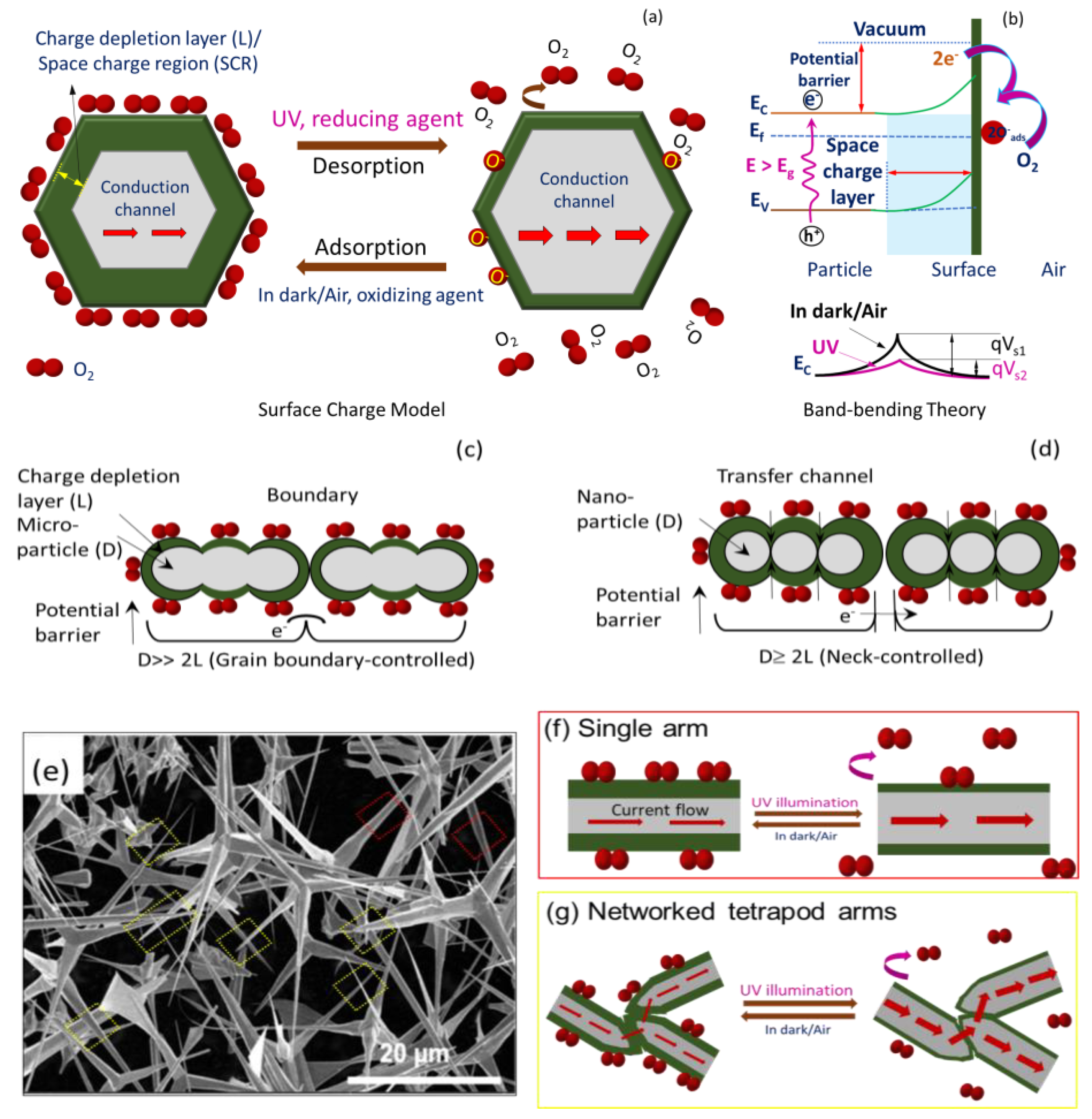
1. Introduction
2. Experimental
2.1. Materials and Methods
2.1.1. Preparation of T–ZnO and Corresponding ZnO-Based Thin Films
2.1.2. Material Characterization and Fabrication of UV Sensor
3. Results and Discussion
3.1. Structural and Morphological Characterization
3.2. Resistance Change Measurements in Controlled UV Environment
3.3. Resistance Change Measurements on Ruminants
4. Conclusions
Author Contributions
Funding
Institutional Review Board Statement
Informed Consent Statement
Data Availability Statement
Acknowledgments
Conflicts of Interest
References
- Miller, R. Oxidative stress and the cardiovascular effects of air pollution. Free Radic. Biol. Med. 2020, 151, 69. [Google Scholar] [CrossRef] [PubMed]
- Fine, G.F.; Cavanagh, L.M.; Afonja, A.; Binions, R. Metal oxide semi-conductor gas sensors in environmental monitoring. Sensors 2010, 10, 5469. [Google Scholar] [CrossRef] [PubMed]
- Wales, D.J.; Grand, J.; Ting, V.P.; Burke, R.D.; Edler, K.J.; Bowen, C.R.; Mintova, S.; Burrows, A.D. Gas sensing using porous materials for automotive applications. Chem. Soc. Rev. 2015, 44, 4290–4321. [Google Scholar] [CrossRef] [PubMed]
- Schraufnagel, D.E.; Balmes, J.R.; Cowl, C.T.; De Matteis, S.; Jung, S.H.; Mortimer, K.; Perez-Padilla, R.; Rice, M.B.; Riojas-Rodriguez, H.; Sood, A.; et al. Air pollution and noncommunicable diseases: A review by the forum of international respiratory societies’ environmental committee. Chest 2019, 155, 417–426. [Google Scholar] [CrossRef] [PubMed]
- Glencross, D.A.; Ho, T.-R.; Camiña, N.; Hawrylowicz, C.M.; Pfeffer, P.E. Air pollution and its effects on the immune system. Free Radic. Biol. Med. 2020, 151, 56–68. [Google Scholar] [CrossRef]
- Zhang, Z.; Xue, T.; Jin, X. Effects of meteorological conditions and air pollution on COVID-19 transmission: Evidence from 219 Chinese cities. Sci. Total Environ. 2020, 741, 140244. [Google Scholar] [CrossRef]
- Garcia, A.; Krummel, G.; Priya, S. Fundamental understanding of millipede morphology and locomotion dynamics. Bioinspir. Biomim. 2021, 16, 026003. [Google Scholar] [CrossRef]
- Chen, Y.; Quinn, J.C.; Weston, L.A.; Loukopoulos, P. The aetiology, prevalence and morbidity of outbreaks of photosensitisation in livestock: A review. PLoS ONE 2019, 14, e0211625. [Google Scholar] [CrossRef]
- Johnson, A.E. Toxicologic Aspects of Photosensitization in Livestock. J. Natl. Cancer Inst. 1982, 69, 253–258. [Google Scholar]
- Saucedo, M.O.; Rodríguez, S.H.S.; Flores, C.F.A.; Valenzuela, R.B.; Luna, M.A.L. Efecto de la radiación ultravioleta (UV) en animales domésticos. Revisión. Rev. Mex. Cienc. Pecu. 2019, 10, 416–432. [Google Scholar] [CrossRef]
- Jaaniso, R.; Tan, O.K. Semiconductor Gas Sensors; Woodhead Publishing Limited: Cambridge, UK, 2013. [Google Scholar]
- Wang, C.; Yin, L.; Zhang, L.; Xiang, D.; Gao, R. Metal oxide gas sensors: Sensitivity and influencing factors. Sensors 2010, 13, 2088. [Google Scholar] [CrossRef]
- Koid, T.; Chichibu, S.F.; Uedono, A.; Sota, T.; Tsukazaki, A.; Kawasaki, M. Radiative and nonradiative excitonic transitions in nonpolar (1120) and polar (0001) and (0001) ZnO epilayers. Appl. Phys. Lett. 2004, 84, 1079–1081. [Google Scholar] [CrossRef]
- Ye, J.D.; Gu, S.L.; Zhu, S.M.; Liu, S.M.; Zheng, Y.D.; Zhang, R.; Shi, Y.; Chen, Q.; Yu, H.Q.; Ye, Y.D. Raman study of lattice dynamic behaviors in phosphorus-doped ZnO films. Appl. Phys. Lett. 2006, 88, 101905. [Google Scholar] [CrossRef]
- Ozgur, U.; Alivov, Y.I.; Liu, C.; Teke, A.; Reshchikov, M.A.; Doğan, S.; Avrutin, V.; Cho, S.-J.; Morkoç, H. A comprehensive review of ZnO materials and devices. J. Appl. Phys. 2005, 98, 041301. [Google Scholar] [CrossRef]
- Razeghi, M.; Rogalski, A. Semiconductor ultraviolet detectors. J. Appl. Phys. 1996, 79, 7433–7473. [Google Scholar] [CrossRef]
- Zou, W.; Sastry, M.; Gooding, J.J.; Ramanathan, R.; Bansal, V. Recent Advances and a Roadmap to Wearable UV Sensor Technologies. Adv. Mater. Technol. 2020, 5, 1901036. [Google Scholar] [CrossRef]
- Lin, T.; Lv, X.; Li, S.; Wang, Q. The Morphologies of the Semiconductor Oxides and Their Gas-Sensing Properties. Sensors 2017, 17, 2779. [Google Scholar] [CrossRef]
- Lao, C.S.; Park, M.-C.; Kuang, Q.; Deng, Y.; Sood, A.K.; Polla, A.D.L.; Wang, Z.L. Giant Enhancement in UV Response of ZnO Nanobelts by Polymer Surface-Functionalization. J. Am. Chem. Soc. 2007, 129, 12096–12097. [Google Scholar] [CrossRef] [PubMed]
- Lupan, O.; Chai, G.; Chow, L. Novel hydrogen gas sensor based on single ZnO nanorod. Microelectron. Eng. 2008, 85, 2220–2225. [Google Scholar] [CrossRef]
- Thepnurat, M.; Ruankham, P.; Phadunghitidhada, S.; Gardchareon, A.; Wongratanaphisan, D.; Choopun, S. Efficient charge-transport UV sensor based on interlinked ZnO tetrapod networks. Surf. Coat. Technol. 2016, 306, 25–29. [Google Scholar] [CrossRef]
- Zheng, K.H.; Zhao, Y.C.; Deng, K.; Liu, Z.; Sun, L.F.; Zhang, Z.X.; Song, L.; Yang, H.F.; Gu, C.Z.; Xie, S.S. Effectively enhanced oxygen sensitivity of individual ZnO tetrapod sensor by water pre-adsorption. Appl. Phys. Lett. 2008, 92, 213116. [Google Scholar] [CrossRef]
- Zhang, Z.; Sun, L.; Zhao, Y.; Liu, Z.; Liu, D.; Cao, L.; Zou, B.; Zhou, W.; Gu, C.; Xie, S. ZnO Tetrapods Designed as Multiterminal Sensors to Distinguish False Responses and Increase Sensitivity. Nano Lett. 2008, 8, 652–655. [Google Scholar] [CrossRef] [PubMed]
- Zhu, C.L.; Chen, Y.J.; Wang, R.X.; Wang, L.J.; Cao, M.S.; Shi, X.L. Synthesis and enhanced ethanol sensing properties of α-Fe2O3/ZnO hetero-nanostructures. Sens. Actuators B 2009, 140, 185. [Google Scholar] [CrossRef]
- Mondal, K.; Islam, M.; Singh, S.; Sharma, A. Fabrication of High Surface Area Microporous ZnO from ZnO/Carbon Sacrificial Composite Monolith Template. Micromachines 2022, 13, 335. [Google Scholar] [CrossRef] [PubMed]
- Mishra, Y.K.; Modi, G.; Cretu, V.; Postica, V.; Lupan, O.; Reimer, T.; Paulowicz, I.; Hrkac, V.; Benecke, W.; Kienle, L.; et al. Direct Growth of Freestanding ZnO Tetrapod Networks for Multifunctional Applications in Photocatalysis, UV Photodetection, and Gas Sensing. ACS Appl. Mater. Interfaces 2015, 7, 14303. [Google Scholar] [CrossRef]
- Mishra, Y.K.; Adelung, R. ZnO Tetrapod Materials for Functional Applications. Mater. Today 2018, 21, 631–651. [Google Scholar] [CrossRef]
- Lupan, O.; Postica, V.; Gröttrup, J.; Mishra, A.K.; de Leeuw, N.H.; Carreira, J.F.C.; Rodrigues, J.; Sedrine, N.B.; Correia, M.R.; Monteiro, T.; et al. Hybridization of Zinc Oxide Tetrapods for Selective Gas Sensing Applications. ACS Appl. Mater. Interfaces 2017, 9, 4084–4099. [Google Scholar] [CrossRef]
- Gröttrup, J.; Paulowicz, I.; Schuchardt, A.; Kaidas, V.; Kaps, S.; Lupan, O.; Adelung, R.; Mishra, Y.K. Three-Dimensional Flexible Ceramics Based on Interconnected Network of Highly Porous Pure and Metal Alloyed ZnO Tetrapods. Ceram. Int. 2016, 42, 8664–8676. [Google Scholar] [CrossRef]
- Zaumseil, P. High-Resolution Characterization of the Forbidden Si 200 and Si 222 Reflections. J. Appl. Crystallogr. 2015, 48, 528–532. [Google Scholar] [CrossRef] [PubMed]
- Kittel, C. Introduction to Solid State Physics, 8th ed.; John Wiley & Sons Inc.: Hoboken, NJ, USA, 1957. [Google Scholar] [CrossRef]
- Jamdagni, P.; Khatri, P.; Rana, J.S. Green Synthesis of Zinc Oxide Nanoparticles Using Flower Extract of Nyctanthes Arbor-Tristis and Their Antifungal Activity. J. King Saud Univ. Sci. 2018, 30, 168–175. [Google Scholar] [CrossRef]
- Cullity, B.D.; Stock, S.R.; Stock, S. Elements of X-Ray Diffraction, 3rd ed.; Pearson: London, UK, 2001. [Google Scholar]
- Boulc’h, F.; Schouler, M.C.; Donnadieu, P.; Chaix, J.M.; Djurado, E. Domain Size Distribution of Y-TZP Nano-Particles Using XRD and HRTEM. Image Anal. Stereol. 2001, 20, 157–161. [Google Scholar] [CrossRef]
- Foo, K.L.; Kashif, M.; Hashim, U.; Liu, W.W. Effect of Different Solvents on the Structural and Optical Properties of Zinc Oxide Thin Films for Optoelectronic Applications. Ceram. Int. 2014, 40 Pt A, 753–761. [Google Scholar] [CrossRef]
- Seetawan, U.; Jugsujinda, S.; Seetawan, T.; Ratchasin, A.; Euvananont, C.; Junin, C.; Thanachayanont, C.; Chainaronk, P. Effect of calcinations temperature on crystallography and nanoparticles in ZnO disk. Mater. Sci. Appl. 2011, 2, 1302–1306. [Google Scholar] [CrossRef]
- Yogamalar, R.; Srinivasan, R.; Vinu, A.; Ariga, K.; Bose, A.C. X-ray peak broadening analysis in ZnO nanoparticles. Sol. State. Commun. 2009, 149, 1919. [Google Scholar] [CrossRef]
- Tagliente, M.A.; Massaro, M. Strain-driven (002) preferred orientation of ZnO nanoparticles in ion-implanted silica, Nucl. Instrum. Methods Phys. Res. B 2008, 266, 1055–1061. [Google Scholar]
- Srikant, V.; Clarke, D.R. On the optical band gap of zinc oxide. J. Appl. Phys. 1998, 83, 5447–5451. [Google Scholar] [CrossRef]
- Salahuddin, N.L.; Kemary, M.; Ibrahim, M. Synthesis, and characterization of ZnO nanoparticles via precipitation method: Effect of annealing temperature on particle size. Nanosci. Nanotechnol. 2015, 5, 82. [Google Scholar]
- Ahmed, T.; Edvinsson, T. Optical Quantum Confinement in Ultrasmall ZnO and the Effect of Size on Their Photocatalytic Activity. J. Phys. Chem. C 2020, 124, 6395–6404. [Google Scholar] [CrossRef]
- Edvinsson, T. Optical quantum confinement and photocatalytic properties in two-, one- and zero-dimensional nanostructures. R. Soc. Open Sci. 2018, 5, 180387. [Google Scholar] [CrossRef]
- Tauc, J.; Grigorovici, R.; Vancu, A. Optical Properties and Electronic Structure of Amorphous Germanium. Phys. Status Solidi 1966, 15, 627–637. [Google Scholar] [CrossRef]
- Wang, M.D.; Zhu, D.Y.; Liu, Y.; Zhang, L.; Zheng, C.X.; He, Z.H.; Chen, D.H.; Wen, L.S. Determination of thickness and optical constants of ZnO thin films prepared by filtered cathode vacuum arc deposition. Chin. Phys. Lett. 2008, 25, 743–746. [Google Scholar]
- Janotti, A.; de Walle, C.G.V. Native point defects in ZnO. Phys. Rev. B 2007, 76, 165202. [Google Scholar] [CrossRef]
- Mooney, P.M. Identification of Defects in Semiconductors; Stavola, M., Ed.; Academic Press: San Diego, CA, USA, 1999; Volume 51B, p. 93. [Google Scholar]
- Hofmann, D.; Pfisterer, D.; Sann, J.; Meyer, B.; Tena-Zaera, R.; Munoz-Sanjose, V.; Frank, T.; Pensl, G. Properties of the oxygen vacancy in ZnO. Appl. Phys. A 2007, 88, 147–151. [Google Scholar] [CrossRef]
- Burlacu, A.; Ursaki, V.V.; Lincot, D.; Skuratov, V.A.; Pauporte, T.; Rusu, E.; Tiginyanu, I.M. Enhanced radiation hardness of ZnO nanorods versus bulk layers. Phys. Status Solidi (RRL) Rapid Res. Lett. 2008, 2, 68–70. [Google Scholar] [CrossRef]
- Auret, F.D.; Goodman, S.A.; Hayes, M.; Legodi, M.J.; Laarhoven, H.A.; Look, D. Electrical Characterization of 1.8 MeV Proton-Bombarded ZnO. Appl. Phys. Lett. 2001, 79, 3074. [Google Scholar] [CrossRef]
- Wang, Z.L. Nanostructures of Zinc Oxide. Mater. Today 2004, 7, 26–33. [Google Scholar] [CrossRef]
- Yoon, Y.; Truong, P.L.; Lee, D.; Ko, S.H. Metal-Oxide Nanomaterials Synthesis and Applications in Flexible and Wearable Sensors. ACS Nanosci. Au 2022, 2, 64–92. [Google Scholar] [CrossRef]
- Kröger, F.A. The Chemistry of Imperfect Crystals, 2nd ed.; North Holland: Amsterdam, The Netherlands, 1974. [Google Scholar]
- Christopher, B.J.; Maksov, A.B.; Muckley, E.S.; Collins, L.; Mahjouri-Samani, M.; Ievlev, A.; Rouleau, C.M.; Moon, J.-W.; Sumpter, B.G.; Ivanov, I.N. UV-activated ZnO films on a flexible substrate for room temperature O2 and H2O sensing. Sci. Rep. 2017, 7, 6053. [Google Scholar] [CrossRef]
- Melnick, D.A. Zinc Oxide Photoconduction, an Oxygen Adsorption Process. J. Chem. Phys. 1957, 26, 1136–1146. [Google Scholar] [CrossRef]
- Soci, C.; Zhang, A.; Xiang, B.; Dayeh, S.A.; Aplin, D.P.R.; Park, J.; Bao, X.Y.; Lo, Y.H.; Wang, D. ZnO Nanowire UV Photodetectors with High Internal Gain. Nano Lett. 2007, 7, 1003–1009. [Google Scholar] [CrossRef]
- Scott, N. Nanotechnology and animal health. Rev. Sci. Tech. 2005, 24, 425–432. [Google Scholar] [CrossRef] [PubMed]


| λex | Sensitivity (ΔR/Rdark) a | Response Time, tr b | Recovery Time, tr b | |
|---|---|---|---|---|
| Bulk ZnO MP | 365 nm | 15% | 0.5 s | 0.4 s |
| Bulk T–ZnO | 365 nm | 43.80% | 0.8 s | 4.2 s |
| Spin–coating | ||||
| ZnO–MP | 302 nm | 15% | 15 ms | 0.5 ms |
| 365 nm | 37% | 2.1 ms | 0.8 ms | |
| ZnO–NP | 302 nm | 16.7% | 372 ms | 3700 ms |
| 365 nm | 35.8% | 1600 ms | 99.4 ms | |
| T–ZnO | 302 nm | 21% | 7.9 ms | 0.9 ms |
| 365 nm | 39% | 3.3 ms | 0.5 ms | |
| Drop-casting | ||||
| ZnO–NP+PVB | 302 nm | 3.5% | 39 s | 18.5 s |
| 365 nm | 3.99% | 0.11 s | 0.282 s | |
| T–ZnO+PVB | 302 nm | 13.7% | 11.1 s | 11.1 s |
| 365 nm | 23.2% | 0.106 s | 0.106 s | |
Publisher’s Note: MDPI stays neutral with regard to jurisdictional claims in published maps and institutional affiliations. |
© 2022 by the authors. Licensee MDPI, Basel, Switzerland. This article is an open access article distributed under the terms and conditions of the Creative Commons Attribution (CC BY) license (https://creativecommons.org/licenses/by/4.0/).
Share and Cite
Knoepfel, A.; Liu, N.; Hou, Y.; Sujani, S.; dos Reis, B.R.; White, R.; Wang, K.; Poudel, B.; Gupta, S.; Priya, S. Development of Tetrapod Zinc Oxide-Based UV Sensor for Precision Livestock Farming and Productivity. Biosensors 2022, 12, 837. https://doi.org/10.3390/bios12100837
Knoepfel A, Liu N, Hou Y, Sujani S, dos Reis BR, White R, Wang K, Poudel B, Gupta S, Priya S. Development of Tetrapod Zinc Oxide-Based UV Sensor for Precision Livestock Farming and Productivity. Biosensors. 2022; 12(10):837. https://doi.org/10.3390/bios12100837
Chicago/Turabian StyleKnoepfel, Abbey, Na Liu, Yuchen Hou, Sathya Sujani, Barbara Roqueto dos Reis, Robin White, Kai Wang, Bed Poudel, Sanju Gupta, and Shashank Priya. 2022. "Development of Tetrapod Zinc Oxide-Based UV Sensor for Precision Livestock Farming and Productivity" Biosensors 12, no. 10: 837. https://doi.org/10.3390/bios12100837
APA StyleKnoepfel, A., Liu, N., Hou, Y., Sujani, S., dos Reis, B. R., White, R., Wang, K., Poudel, B., Gupta, S., & Priya, S. (2022). Development of Tetrapod Zinc Oxide-Based UV Sensor for Precision Livestock Farming and Productivity. Biosensors, 12(10), 837. https://doi.org/10.3390/bios12100837