Microfluidic Packaging Integration with Electronic-Photonic Biosensors Using 3D Printed Transfer Molding

 , , ,
, , , 
Abstract
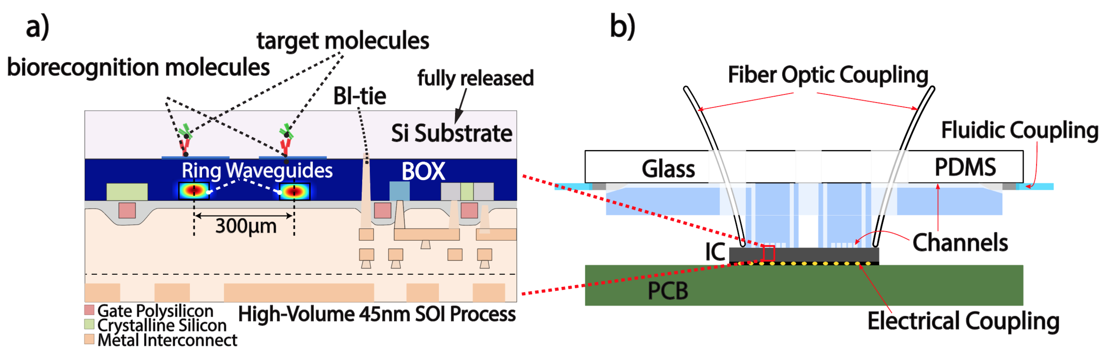
1. Introduction
2. Materials and Methods
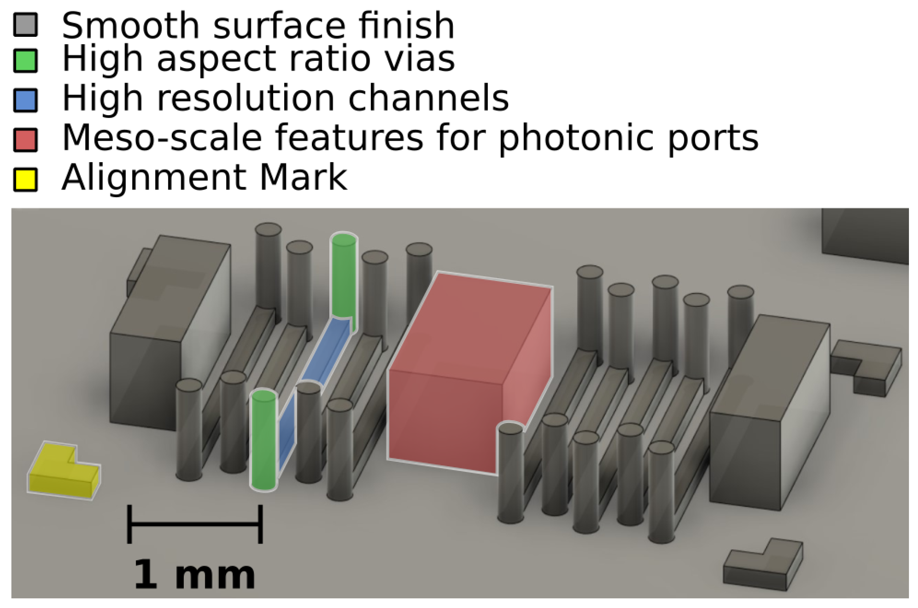
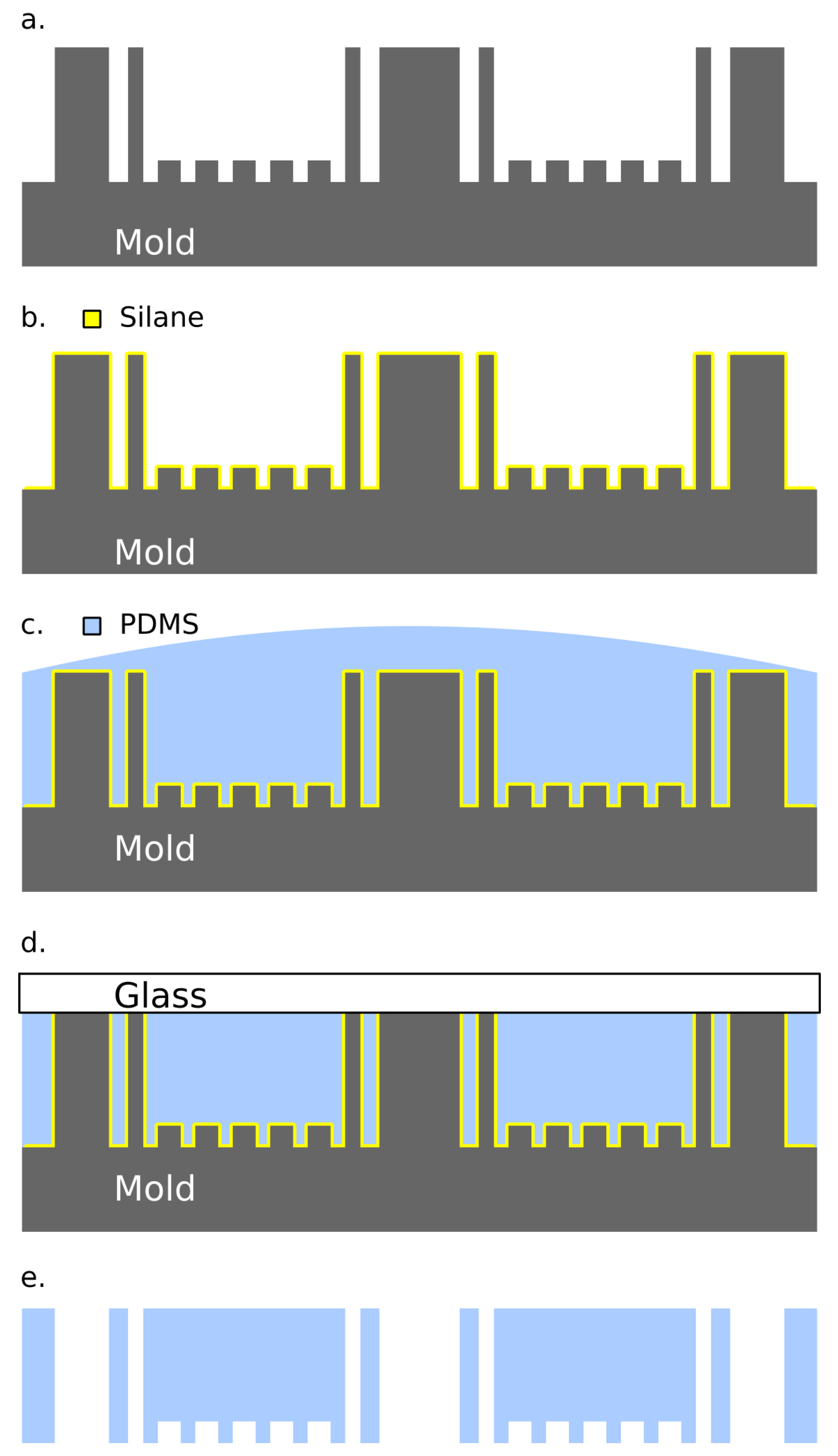
2.1. 3D Printed Mold Fabrication
2.2. Microfluidic Device Casting
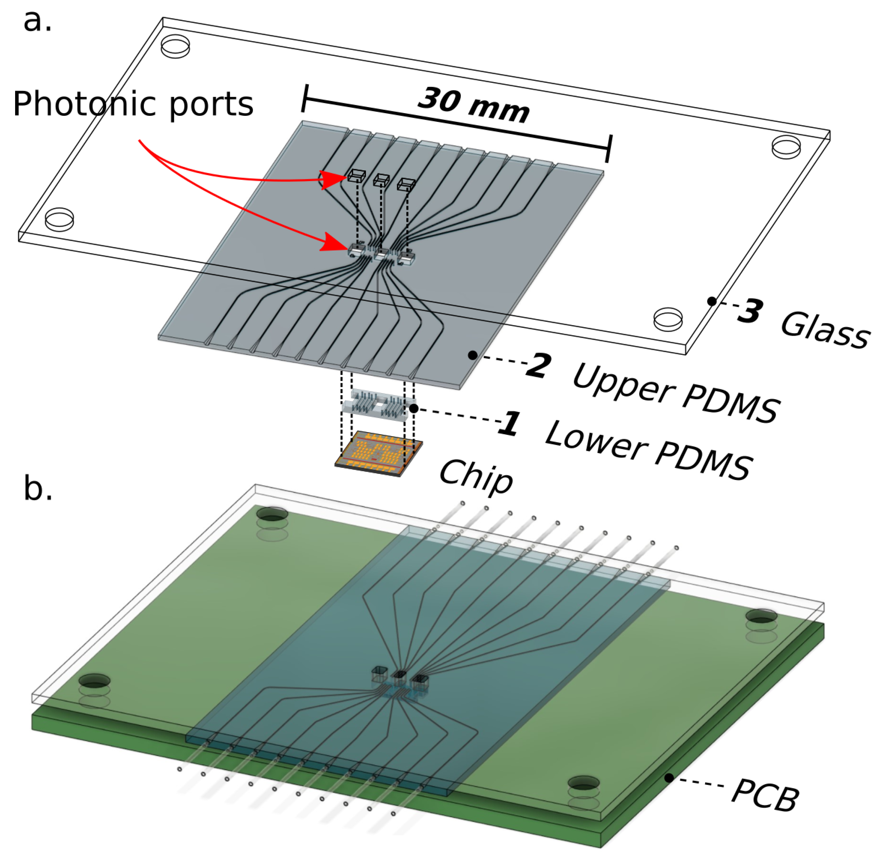
2.3. Alignment and Mechanical Sealing
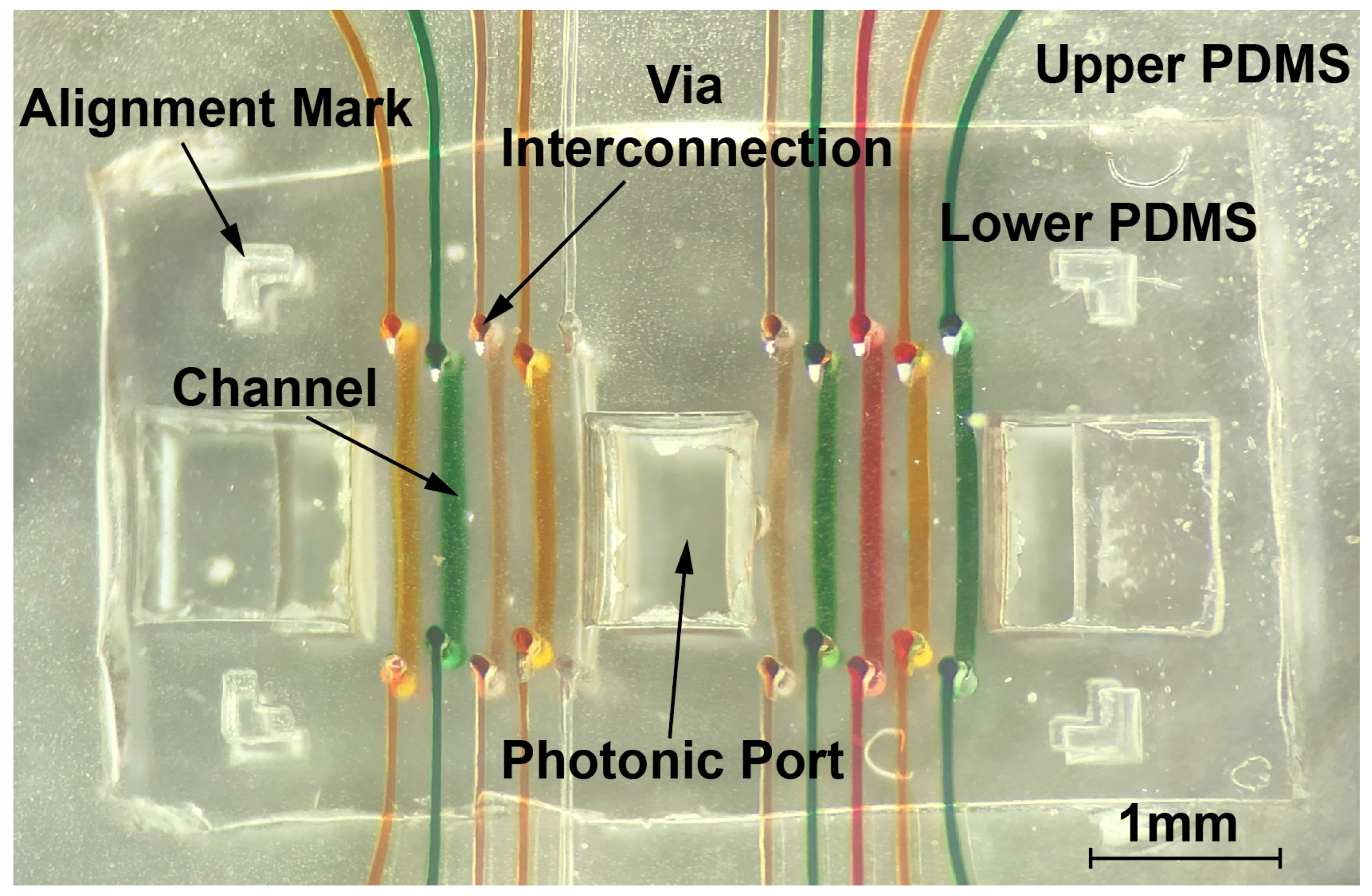
3. Results and Discussions
3.1. Microfluidic Validation—Dye Test
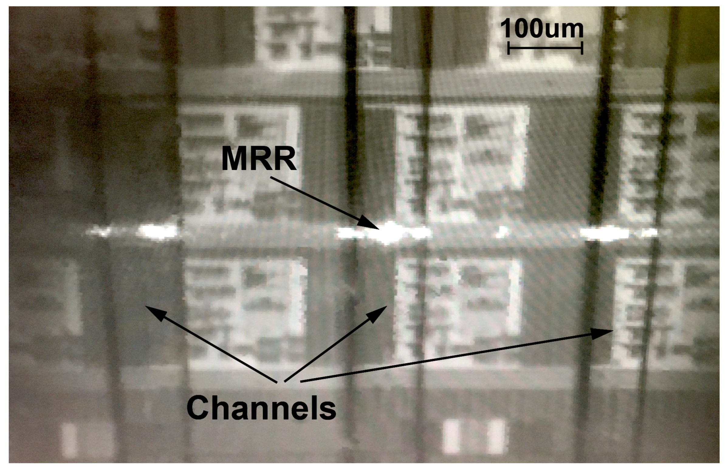
3.2. Photonic Coupling and Bulk Sensitivity
4. Conclusions
Funding
Acknowledgments
Conflicts of Interest
References
- Yang, C.-Y.; Brooks, E.; Li, Y.; Denny, P.; Ho, C.-M.; Qi, F.; Shi, W.; Wolinsky, L.; Wu, B.; Wong, D.T.W.; et al. Detection of picomolar levels of interleukin-8 in human saliva by SPR. Lab Chip 2005, 5, 1017–1023. [Google Scholar] [CrossRef] [PubMed]
- Jason-Moller, L.; Murphy, M.; Bruno, J. Overview of Biacore systems and their applications. Curr. Protoc. Protein Sci. 2006, 45, 19.13.1–19.13.14. [Google Scholar] [CrossRef] [PubMed]
- Gopinath, S. Biosensing applications of surface plasmon resonance-based Biacore technology. Sens. Actuators B Chem. 2010, 150, 722–733. [Google Scholar] [CrossRef]
- Washburn, A.L.; Luchansky, M.S.; Bowman, A.L.; Bailey, R.C. Quantitative, Label-Free Detection of Five Protein Biomarkers Using Multiplexed Arrays of Silicon Photonic Microring Resonators. Anal. Chem. 2010, 82, 69–72. [Google Scholar] [CrossRef] [PubMed]
- Washburn, A.L.; Gunn, L.C.; Bailey, R.C. Label-free quantitation of a cancer biomarker in complex media using silicon photonic microring resonators. Anal. Chem. 2009, 81, 9499–9506. [Google Scholar] [CrossRef]
- Luchansky, M.S.; Washburn, A.L.; McClellan, M.S.; Bailey, R.C. Sensitive on-chip detection of a protein biomarker in human serum and plasma over an extended dynamic range using silicon photonic microring resonators and sub-micron beads. Lab Chip 2011, 11, 2042–2044. [Google Scholar] [CrossRef]
- Qavi, A.J.; Kindt, J.T.; Gleeson, M.A.; Bailey, R.C. Anti-DNA:RNA Antibodies and Silicon Photonic Microring Resonators: Increased Sensitivity for Multiplexed microRNA Detection. Anal. Chem. 2011, 83, 5949–5956. [Google Scholar] [CrossRef]
- Iqbal, M.; Gleeson, M.A.; Spaugh, B.; Tybor, F.; Gunn, W.G.; Hochberg, M.; Baehr-Jones, T.; Bailey, R.C.; Gunn, L.C. Label-Free Biosensor Arrays Based on Silicon Ring Resonators and High-Speed Optical Scanning Instrumentation. IEEE J. Sel. Top. Quantum Electron. 2010, 16, 654–661. [Google Scholar] [CrossRef]
- Flueckiger, J.; Schmidt, S.; Donzella, V.; Sherwali, A.; Ratner, D.M.; Chrostowski, L.; Cheung, K.C. Sub-wavelength grating for enhanced ring resonator biosensor. Opt. Express 2016, 24, 15672. [Google Scholar] [CrossRef]
- Yan, H.; Huang, L.; Xu, X.; Chakravarty, S.; Tang, N.; Tian, H.; Chen, R.T. Unique surface sensing property and enhanced sensitivity in microring resonator biosensors based on subwavelength grating wave- guides. Opt. Express. 2016, 24, 29724–29733. [Google Scholar] [CrossRef]
- Adamopoulos, C.; Gharia, A.; Niknejad, A.; Anwar, M.; Stojanović, V. Electronic-Photonic Platform for Label-Free Biophotonic Sensing in Advanced Zero-Change CMOS-SOI Process. In Proceedings of the Conference on Lasers and Electro-Optics, OSA, San Jose, CA, USA, 5–10 May 2019; p. JW2A.81. [Google Scholar] [CrossRef]
- Claes, T.; Molera, J.G.; De Vos, K.; Schacht, E.; Baets, R.; Bienstman, P. Label-Free Biosensing With a Slot-Waveguide-Based Ring Resonator in Silicon on Insulator. IEEE Photonics J. 2009, 1, 197–204. [Google Scholar] [CrossRef]
- Vos, K.D.; Girones, J.; Claes, T.; Koninck, Y.D.; Popelka, S.; Schacht, E.; Baets, R.; Bienstman, P. Multiplexed Antibody Detection With an Array of Silicon-on-Insulator Microring Resonators. IEEE Photonics J. 2009, 1, 225–235. [Google Scholar] [CrossRef]
- Khan, S.; Gumus, A.; Nassar, J.; Hussain, M. CMOS Enabled Microfluidic Systems for Healthcare Based Applications. Adv. Mater. 2018, 30, 1705759. [Google Scholar] [CrossRef] [PubMed]
- Muluneh, M.; Issadore, D. A multi-scale PDMS Fabrication strategy to bridge the size mismatch between integrated circuits and microfluidics. Lab Chip 2014, 14, 4552–4558. [Google Scholar] [CrossRef] [PubMed]
- Wu, H.; Odom, T.; Chiu, D.; Whitesides, G. Fabrication of complex three-dimensional microchannel systems in PDMS. J. Am. Chem. Soc. 2003, 125, 554–559. [Google Scholar] [CrossRef] [PubMed]
- Comina, G.; Suska, A.; Filippini, D. PDMS lab-on-a-chip fabrication using 3D printed templates. Lab Chip 2014, 14, 424–430. [Google Scholar] [CrossRef] [PubMed]
- Qin, D.; Xia, Y.; Whitesides, G. Soft lithography for micro- and nanoscale patterning. Nat. Protoc. 2010, 5, 491–502. [Google Scholar] [CrossRef]
- Zhang, M.; Wu, J.; Wang, L.; Xiao, K.; Wen, W. A simple method for fabricating multi-layer PDMS structures for 3D microfluidic chips. Lab Chip 2010, 10, 1199. [Google Scholar] [CrossRef]
- Friend, J.; Yeo, L. Fabrication of microfluidic devices using polydimethylsiloxane. Biomicrofluidics 2010, 4, 026502. [Google Scholar] [CrossRef]
- Bhattacharya, S.; Datta, A.; Berg, J.M.; Gangopadhyay, S. Studies on surface wettability of poly(dimethyl) siloxane (PDMS) and glass under oxygen-plasma treatment and correlation with bond strength. J. Microelectromech. Syst. 2005, 14, 590–597. [Google Scholar] [CrossRef]
- Bogaerts, W.; de Heyn, P.; van Vaerenbergh, T.; de Vos, K.; Selvaraja, S.K.; Claes, T.; Dumon, P.; Bienstman, P.; van Thourhout, D.; Baets, R. Silicon microring resonators. Las. Photon. 2012, 6, 590–597. [Google Scholar] [CrossRef]


Publisher’s Note: MDPI stays neutral with regard to jurisdictional claims in published maps and institutional affiliations. |
© 2020 by the authors. Licensee MDPI, Basel, Switzerland. This article is an open access article distributed under the terms and conditions of the Creative Commons Attribution (CC BY) license (http://creativecommons.org/licenses/by/4.0/).
Share and Cite
Adamopoulos, C.; Gharia, A.; Niknejad, A.; Stojanović, V.; Anwar, M. Microfluidic Packaging Integration with Electronic-Photonic Biosensors Using 3D Printed Transfer Molding. Biosensors 2020, 10, 177. https://doi.org/10.3390/bios10110177
Adamopoulos C, Gharia A, Niknejad A, Stojanović V, Anwar M. Microfluidic Packaging Integration with Electronic-Photonic Biosensors Using 3D Printed Transfer Molding. Biosensors. 2020; 10(11):177. https://doi.org/10.3390/bios10110177
Chicago/Turabian StyleAdamopoulos, Christos, Asmaysinh Gharia, Ali Niknejad, Vladimir Stojanović, and Mekhail Anwar. 2020. "Microfluidic Packaging Integration with Electronic-Photonic Biosensors Using 3D Printed Transfer Molding" Biosensors 10, no. 11: 177. https://doi.org/10.3390/bios10110177
APA StyleAdamopoulos, C., Gharia, A., Niknejad, A., Stojanović, V., & Anwar, M. (2020). Microfluidic Packaging Integration with Electronic-Photonic Biosensors Using 3D Printed Transfer Molding. Biosensors, 10(11), 177. https://doi.org/10.3390/bios10110177