Article

Improvement of the Bias Stress Stability in 2D MoS2 and WS2 Transistors with a TiO2 Interfacial Layer

1
Department of Advanced Material Engineering, Chungbuk National University, Chungdae-ro 1, Seowon-Gu, Cheongju, Chungbuk 28644, Korea
2
Department of Nanobio Materials and Electronics, GIST, 123 Cheomdan-gwagiro, Buk-gu, Gwangju 61005, Korea
3
Materials Center for Energy Department, Surface Technology Division, Korea Institute of Materials Science (KIMS), 797 Changwondaero, Sungsan-gu, Changwon, Gyeongnam 51508, Korea
*
Author to whom correspondence should be addressed.
These authors contributed equally to this work.
Nanomaterials 2019, 9(8), 1155; https://doi.org/10.3390/nano9081155
Submission received: 11 July 2019 / Revised: 1 August 2019 / Accepted: 8 August 2019 / Published: 12 August 2019
(This article belongs to the Special Issue Preparation and Properties of 2D Materials)

Abstract

:
The fermi-level pinning phenomenon, which occurs at the metal–semiconductor interface, not only obstructs the achievement of high-performance field effect transistors (FETs) but also results in poor long-term stability. This paper reports on the improvement in gate-bias stress stability in two-dimensional (2D) transition metal dichalcogenide (TMD) FETs with a titanium dioxide (TiO2) interfacial layer inserted between the 2D TMDs (MoS2 or WS2) and metal electrodes. Compared to the control MoS2, the device without the TiO2 layer, the TiO2 interfacial layer deposited on 2D TMDs could lead to more effective carrier modulation by simply changing the contact metal, thereby improving the performance of the Schottky-barrier-modulated FET device. The TiO2 layer could also suppress the Fermi-level pinning phenomenon usually fixed to the metal–semiconductor interface, resulting in an improvement in transistor performance. Especially, the introduction of the TiO2 layer contributed to achieving stable device performance. Threshold voltage variation of MoS2 and WS2 FETs with the TiO2 interfacial layer was ~2 V and ~3.6 V, respectively. The theoretical result of the density function theory validated that mid-gap energy states created within the bandgap of 2D MoS2 can cause a doping effect. The simple approach of introducing a thin interfacial oxide layer offers a promising way toward the implementation of high-performance 2D TMD-based logic circuits.

Graphical Abstract

1. Introduction

The process of extreme scaling-down to reach a physical channel length limit of sub-100 nm has caused critical problems, such as a short channel effect and increased leakage current. To address these limitations, efforts have recently been made to scrutinize promising semiconducting materials. In particular, atomically thin layered transition metal dichalcogenides (TMDs) have attracted great attention due to their extraordinary electrical, optical, and mechanical properties [1,2,3,4,5,6,7,8,9]. One of their most attractive properties is the existence of a band-gap and its facile engineering. For instance, single-layer molybdenum disulfide (MoS2) has a direct band-gap of ~1.8 eV, and multilayer MoS2 has an indirect band-gap of ~1.2 eV [1]. The physical properties of 2D TMDs have led to their applications in various electronic devices such as transistors, memory devices, and opto-electronic devices [10,11,12,13,14,15,16,17,18]. Among them, the most promising device is the field caused effect transistor (FET), which functions as an essential switching component of display back-plane circuits [12].
However, a few challenging issues around employing 2D TMD-based FETs for practical applications have to be resolved. Fabricating large-scale, high-quality continuous 2D TMD films and the direct deposition of the gate dielectric layer on a 2D surface with a low surface energy are important issues in terms of the utilization of conventional Si fabrication infrastructures and the realization of high-mobility FETs. Furthermore, the unreliable performance of 2D TMD FETs has been a critical concern that must be preferentially addressed. Chemically and mechanically disordered surface and interface states are the origin of the performance instability of semiconductor devices, causing a large hysteresis window and a significant threshold voltage (VTH) shift.
The passivation of the polymer layer on the 2D TMDs is an efficient countermeasure against the instability of 2D semiconductor-based FET performance [19,20]. Using a similar method, Zheng et al. reported that the hysteresis window of the 2D layered materials capped with an Al2O3 was considerably reduced [20]. Meanwhile, the contact engineering strategy for modifying the interface states between a metal and a 2D semiconductor has been actively studied [21,22,23,24,25,26,27,28]. Because the operation of the 2D TMD FET is based on a modulation of the Schottky-barrier, the interface quality at the metal/TMD contact becomes more critical. Several approaches to reduce the contact resistance, including a doping technique and selection of proper work function metal, have been proposed [26,28]. Meanwhile, Fermi-level pinning usually occurs at a metal/semiconductor contact region, causing high contact resistance due to a fixed high band offset regardless of the work function value of the metal [25,26,29]. Because the interface states usually serve as carrier trapping sites, it is hard to realize the high performance of 2D TMD FETs. Thus, a reliable and simple approach for Fermi-level depinning is necessary. The corresponding result was reported for an MoS2 device with an interfacial oxide layer [29].
Herein, the effect of the interfacial buffer layer at the metal/2D TMD (MoS2 and WS2) contact on transistor performance was experimentally and theoretically investigated. Titanium dioxide (TiO2) was used as a buffer layer because its band offset with MoS2 and WS2 is relatively small and tunnel resistance can be minimized with the thin TiO2 layer. By employing a TiO2 interlayer, interface states were successfully reduced, achieving an increased drive current and the enhancement of long term bias stress stability. In addition, the role of the TiO2 layer on MoS2 was theoretically elucidated using a density function theory (DFT) simulation. It can be highlighted that we suggested a facile approach to achieve both higher transistor performance and stability at the same time.

2. Materials and Methods

A mechanical exfoliation method using scotch tape to obtain high-quality 2D TMD flakes was adopted, and then the exfoliated 2D TMD flakes (MoS2 and WS2) were transferred onto a SiO2 (300 nm)/heavily doped Si substrate. To identify the existence of the 2D TMDs, MoS2 was mechanically exfoliated from the bulk mineral, and the multilayer MoS2 was characterized using Raman spectroscopy (Figure 1a). LabRAM ARAMIS (laser wavelength: 473 nm, 50 mW) was used for Raman measurements. Two prominent peaks feature the in-plane E12g mode (~384 cm−1) and the out-of-plane A1g mode (~409 cm−1) of the MoS2. A frequency difference of ~25 cm−1 between two vibrational modes indicates a multilayer MoS2. To determine the thickness of the exfoliated MoS2, we performed an atomic force microscopy (AFM) analysis. As shown in Figure 1b, the 92 nm-thick MoS2 was transferred onto the SiO2/Si substrate using a typical scotch-tape exfoliation method.
To investigate the effect of the TiO2 interlayer on the device’s contact properties, 2D FET devices with back gate electrodes were fabricated: a control device without TiO2 and a testing device with TiO2. Figure 1c shows the 3D schematic image of the FET device with the 2D TMD-TiO2-Ti/Au structure. The TiO2 interfacial layer on the 2D TMDs was deposited using an atomic layer deposition (ALD) technique based on a tetrakis-dimethyl-amido-titanium (TDMAT) precursor at 200 °C. The pulse and purging times were 0.2 s and 20 s, respectively. The number of cycles were 15, resulting in a 2~3 nm thickness. The thickness of the TiO2 layer was also optimized to avoid high tunnel resistance. The 2D TMD transistor devices were made by a conventional photolithography process. Photolithography was conducted after spin-coating of the photoresist (AZ 5214, MicroChemicals, Germany), and the metal was deposited by a physical vapor evaporator. Electron beam evaporation was selected to minimize the physical damage on the surface of the TMDs. Lift-off processes were sequentially performed to make the source and drain electrodes. The channel distance between source and drain was ~3 μm. After device fabrication, the post-annealing process was conducted in a vacuum environment at 300 °C. The process of the vacuum annealing step included a 30 min ramping time to 300 °C, for a 1 h duration, and a cool down at room temperature. The electrical characterization (transfer, output, and stress measurement) was performed with a Keithley 4200-SCS (Keithley, Cleveland, OH, US). Stress measurement followed the conventional stress-measure-stress sequence for 10,000 s, which is summarized in Figure S6 of the Supplementary Materials information.
Figure 1d shows a cross-sectional high-resolution transmission electron microscopy (HRTEM) image of the MoS2-TiO2-Ti stacked structure. The lattice constant of the MoS2 was measured to be ~0.65 nm along the c-plane [0001] direction in a hexagonal close-packed crystal structure. A thin (~3 nm-thick) TiO2 layer, deposited using the atomic layer deposition process, was inserted between the Ti metal and MoS2. Interestingly, the discontinuous layers of the MoS2 layers exhibited a step-like crystal structure. Thus, it is reasonably expected that randomness in the defect density for the exposed edge planes and basal planes can cause considerable deviation from the physical interface states, thereby inducing a large difference in the electrical properties of MoS2. The structural disorder of the MoS2 surface is also a strong source for Fermi-level pinning, which caused some points of the band gap to be locked (pinned) to the Fermi-level. This made the Schottky-barrier height considerably insensitive to the metal’s work function. The Fermi-level pinning phenomenon, with respect to various metals (for instance, Ti, Cr, Au, and Pd), is illustrated in Figure S1 in the Supplementary Materials information. Even in the corresponding literature studies, the existence of dangling bonds in TMD has been proven via in-depth analyses, such as scanning tunneling microscopy and inductively coupled plasma-mass spectroscopy [30,31,32,33].

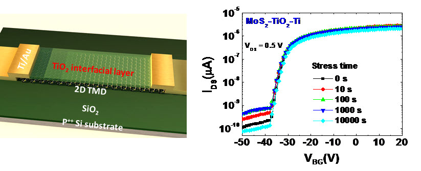
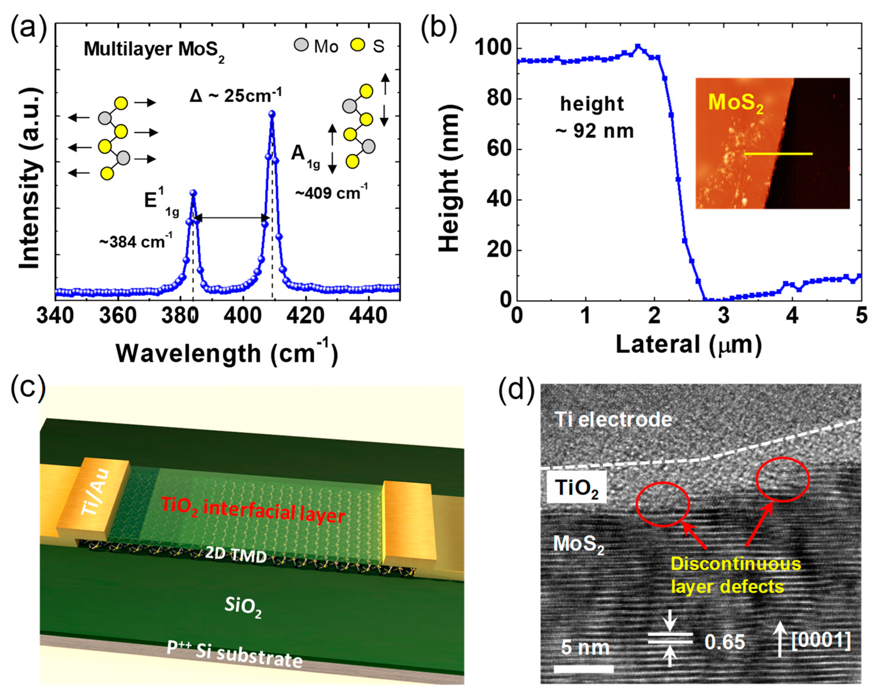
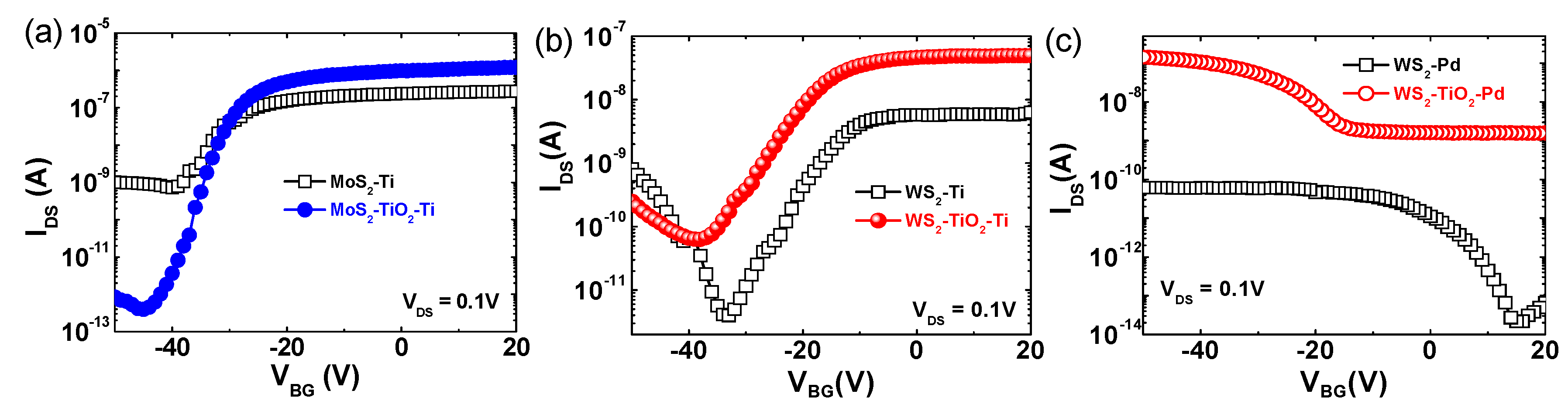
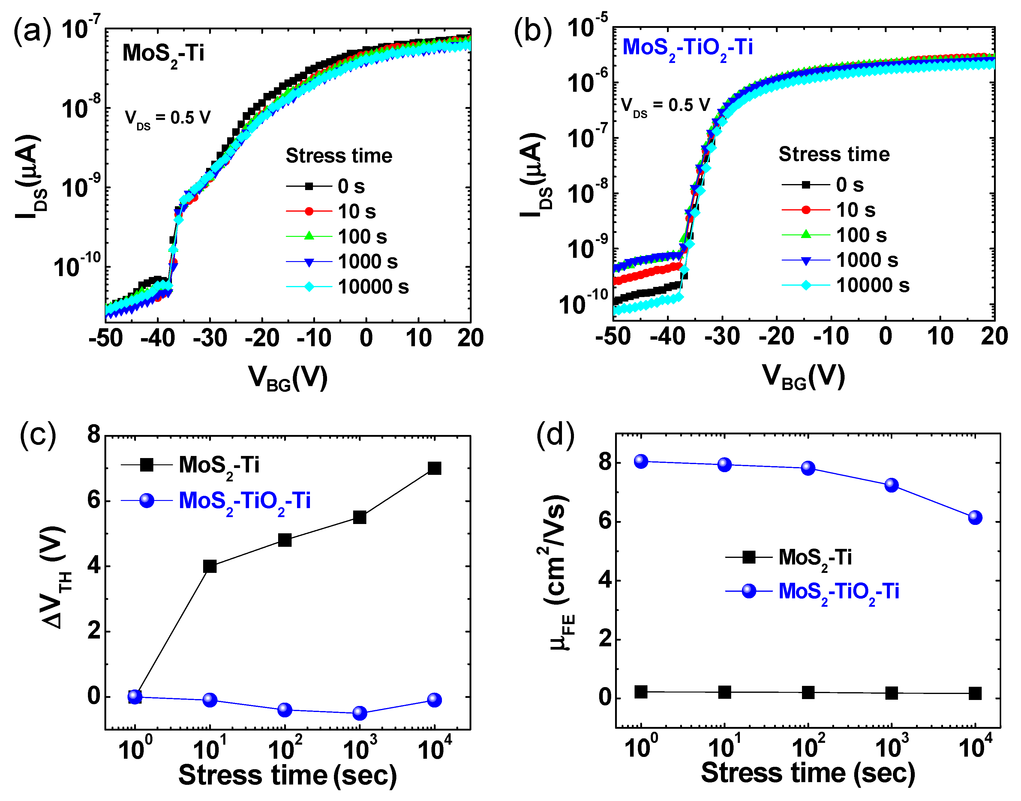
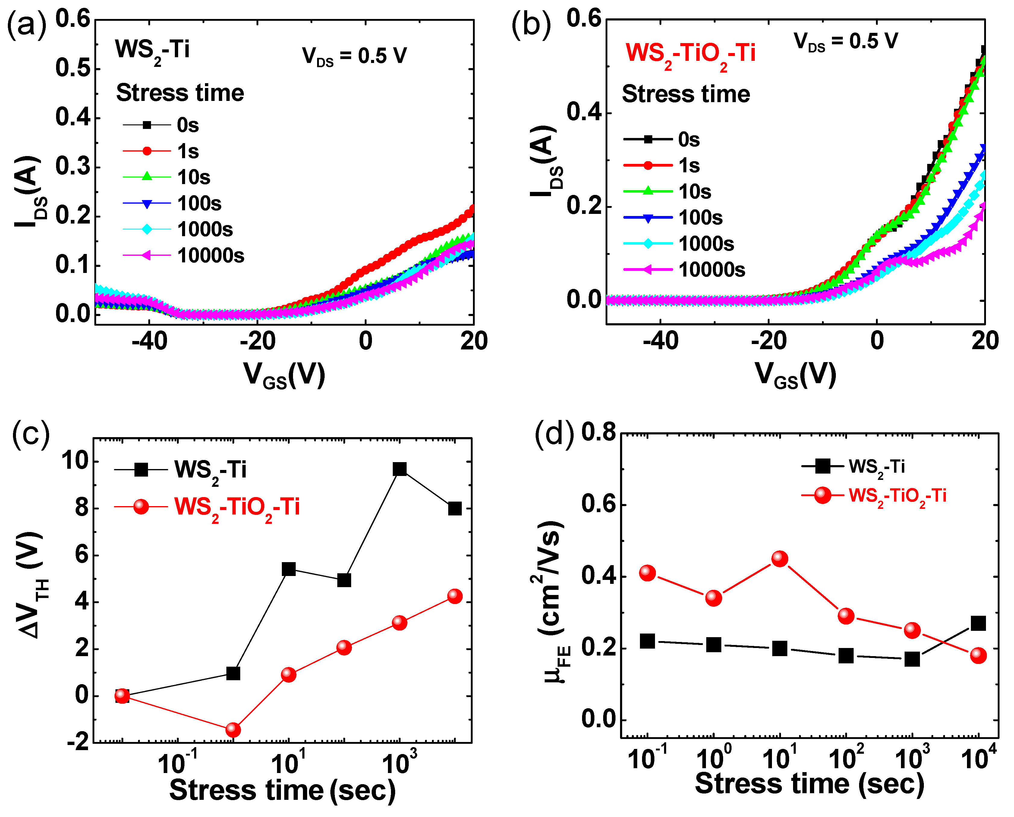
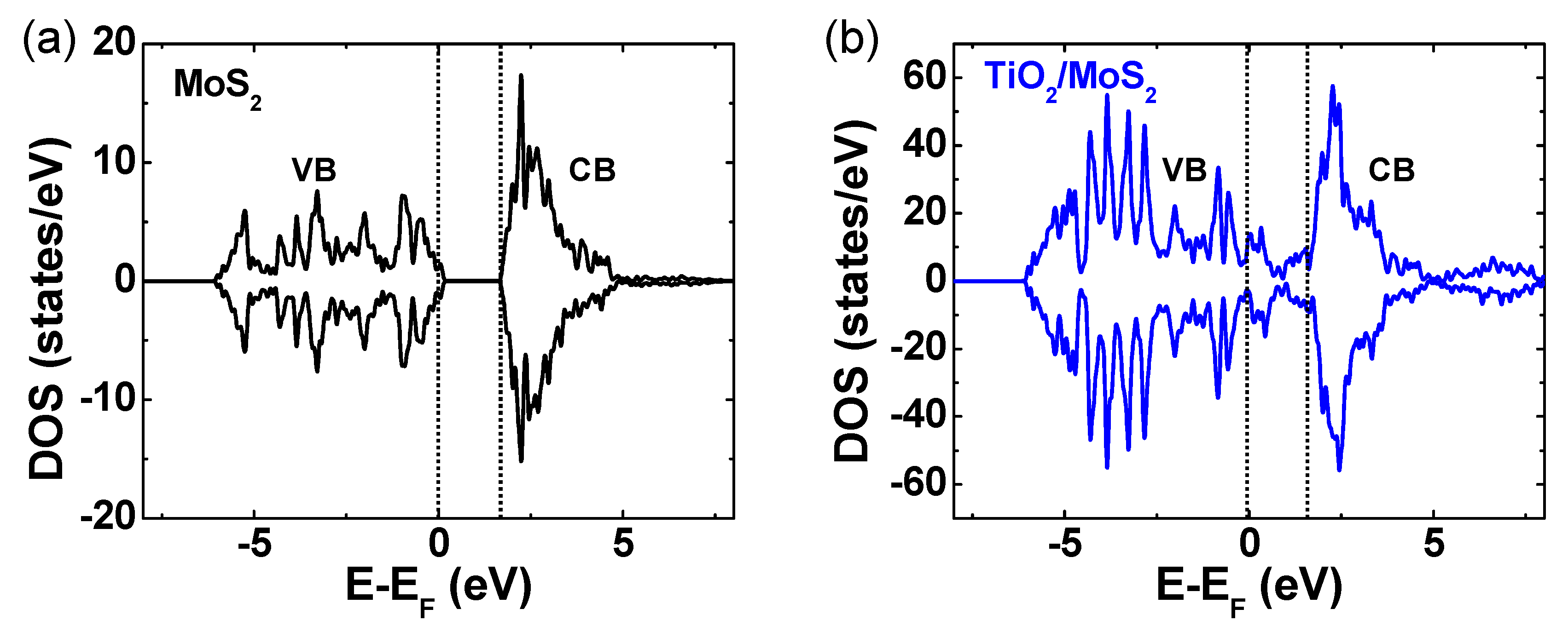
3. Results and Discussion

To investigate the influence of a TiO2 interfacial layer on the MoS2 and WS2 device performance, electrical measurements were performed. Basic electrical characterizations were carried out with a Keithley 4200-SCS (Keithley, Cleveland, OH, US) analyzer. Figure 2a shows a comparison between the transfer characteristics (IDS-VBG) of the MoS2-Ti and MoS2-TiO2-Ti devices. The gate-bias sweeping ranged from −50 to 20 V at a fixed drain voltage of 0.1 V. A typical unipolar n-type behavior and a depletion mode of MoS2 transistor devices were observed. The MoS2-TiO2-Ti device with a TiO2 interfacial layer showed more enhanced performance with a higher drive on current (ION). ION values for devices without and with the TiO2 layer are 0.36 and 1.22 µA, respectively. The field effect mobility (μFE) values for MoS2-Ti and MoS2-TiO2-Ti devices were estimated to be 1.38 and 6.08 cm2/V·s, respectively. The transfer curves at variable drain voltages and output characteristic also confirmed the better performance of the testing devices with the TiO2 layer (Figure S2 in the Supplementary Materials information). The μFE values of the MoS2-TiO2-Ti device as a function of gate voltage were higher than those of the MoS2-Ti device (Figure S3 in the Supplementary Materials information).
A more interesting result was observed on the WS2 FETs. Figure 2b shows a comparison of the IDS-VBG transfer characteristics of the WS2-Ti and WS2-TiO2-Ti structured devices. The bi-polar behavior of the WS2-Ti structured devices was observed, which is consistent with the previous results [34]. It is highly likely that the Fermi-level of the Ti metal exists within the mid-gap of WS2. The transfer curve of the WS2-TiO2-Ti structured device showed stronger n-type unipolar behavior with a higher ION current than that of the WS2-Ti device. As shown in Figure 2c, we also characterized the WS2 devices using Pd metal electrodes with a relatively high work function of ~5.1 eV to understand the mid-gap pinning and the effects of an interfacial layer. The addition of the TiO2 layer on the WS2 caused a change from a weak bipolar to a p-type unipolar behavior. This result indicates that a high Schottky-barrier can be effectively reduced by a contact engineering approach utilizing a very thin TiO2 interfacial layer. The IDS-VBG curves of the WS2 FETs at various drain voltages are also shown in Figure S4 of the Supplementary Materials information. The performance enhancement of the 2D FET devices with the interfacial TiO2 layer is attributed to the considerable reduction in the density of the diverse interface states, resulting from the direct contact between the metal and the 2D semiconductor channel. Comparison of the proposed band diagrams between the 2D TMD-Ti and 2D TMD-TiO2-Ti devices highlights the change in the Schottky-barrier height as shown in Figure S5 in the Supplementary Materials information. In principle, the theoretical Fermi-level alignment between the metal and semiconductor, called Fermi-level depinning, also creates a more effective carrier modulation of the 2D TMD FET device.
For practical transistor applications, the electrical stability of the MoS2 based FET devices was examined under a long-term positive gate-bias stress condition, as shown in Figure 3a–d. Figure 3a,b shows the shift of the IDS-VBG curves during the long-term gate-bias stress test. The transfer I-V curve properties were monitored every logarithmic time interval (1, 10, 100, 1000, and 10,000 s) while continuously applying +10 V to the gate electrode. Schemes to illustrate the stress measurement set up environment and the data checking points are shown in Figure S6 of the Supplementary Materials information. Even if the IDS-VBG curves in all of the MoS2-Ti and MoS2-TiO2-Ti devices were slightly shifted to the positive direction, the device with the TiO2 layer showed less of a shift than that without TiO2, indicating more stable electrical properties compared to the control device without TiO2. Interestingly, in Figure 3b, the variation of IOFF values for the MoS2-TiO2-Ti stack seems more severe than that of the control MoS2-Ti device. The actual differences of the minimum and maximum IOFF values are 4.20 × 10⁻¹² A and 3.68 × 10⁻¹⁰ A for MoS2-Ti and MoS2-TiO2-Ti, respectively. The IOFF fluctuation of all the devices was less than 1 nA, and this fluctuation was negligible in operation. Figure 3c shows a summary of the threshold voltage (VTH) change for MoS2-Ti and MoS2-TiO2-Ti stacked devices as a function of stress time, which was extracted from the raw data from Figure 3a,b. The MoS2 FET without a TiO2 layer showed a more positive VTH shift than that of the MoS2 FET with a TiO2 layer. The VTH shift for the MoS2 FET without and with a TiO2 interfacial layer was 3.1 and 1.1 V, respectively. The TiO2 layer could serve as a buffer layer to mitigate the interfacial damage from electrical stress. As shown in Figure 3d, we also compared the field-effect mobility (μFE) values for the devices without and with a TiO2 layer. The μFE was estimated by following equation:
μ F E = g m L W 1 V D S 1 C o x   and   g m = I D V G
where gm is the maximum transconductance that can be achieved from IDS-VBG, L is the channel length, W is the channel width, VDS is the applied drain bias, and Cox is the gate oxide capacitance.
Overall, the μFE of MoS2-TiO2-Ti device was higher than that of the MoS2-Ti device. After 10,000 s stress time, the μFE was reduced from 0.22 to 0.17 cm2/Vs for the device without a TiO2 layer and from 8.05 to 6.14 cm2/Vs for the device with a TiO2 layer. Approximately, 25% of the μFE reduction was observed for both cases.
Additionally, the stability of the contact region for the WS2-based FET devices was also determined for the effect of the interfacial TiO2 layer on bias stress stability, as shown in Figure 4a,b. As can be seen, the transfer curves of the WS2-Ti contact FET device showed bipolar behavior where both electron and hole carriers contribute to the current flow of the semiconductor channel. Overall, a lower VTH shift was observed for the FET with a TiO2 layer compared to the FET without a TiO2 layer, indicating that the introduction of the TiO2 interfacial layer on the WS2 layered film is also an effective approach for improving the contact reliability of the WS2 device, as well as the case of MoS2 device. Specifically, the VTH shifts for the WS2 FET without and with a TiO2 interfacial layer were 8 and 4.3 V, respectively (Figure 4c). As shown in Figure 4d, the change of μFE as a function of stress time was also fitted: the mobility value was almost unchanged for the control device without a TiO2 layer and from 0.41 to 0.18 cm2/Vs for the testing device with a TiO2 layer.
Indeed, the WS2 FET device was more vulnerable to electrical stress than MoS2, which might be due to greater number of interface states at the metal/semiconductor contact. The metal-induced gap states indispensably exist on the metal/semiconductor interface, which induces the instability of transistor performance. Additionally, there is a quantum mechanically long distance of 2–3 Å between the metal and 2D TMD, which increases the tunneling probability of charge carriers [35]. The more stable performance of the 2D TMD devices with an insulating TiO2 layer might be understood by a mitigation of those gap states and a reduction in physical distance.
To unveil how the TiO2 layer electronically influences the MoS2 semiconductor, we explored a theoretical simulation of electronic states for free-standing MoS2 and MoS2/TiO2 materials via a density functional theory (DFT) calculation (Figure 5). The density of states (DOS) calculation result of the free standing MoS2 showed the existence of a forbidden gap (Figure 5a). Meanwhile, the TiO2/MoS2 hybrid combination featured a spin-polarized metallic behavior. The calculated DOS clearly validates that the addition of the TiO2 layer leads to the modification of the electronical band structure of the junction region, offering the benefit of a doping effect on MoS2.

4. Conclusions

The effect of a TiO2 interfacial layer on metal/TMD (MoS2 and WS2) contact was experimentally and theoretically studied. The advantages of a Schottky-type FET device, possibly implemented according to the value of a metal work function, were achieved in the 2D TMD devices with a TiO2 layer. Furthermore, a more enhanced and stable electrical performance for the 2D TMD FET devices with the TiO2 interfacial layer could be obtained under a gate-bias stress condition. The TiO2 interfacial layer could serve as a Fermi-level de-pinning layer, reducing the density of the interface states. Additionally, the DFT calculation validates the doping effect of the TiO2 interfacial layer on the 2D MoS2. The strategy of inserting a very thin insulating layer into the contact region will be also applied to diverse 2D TMD-based FET devices.

Supplementary Materials

The following are available online at https://www.mdpi.com/2079-4991/9/8/1155/s1, Figure S1: Fabrication process and band diagram for Fermi-level pinning with various metals; Figure S2: Transfer and output curves for MoS2 FETs without and with a TiO2 layer; Figure S3: Field-effect mobility (μFE) for MoS2 FETs without and with a TiO2 layer; Figure S4: Transfer curves for WS2-Ti, WS2-TiO2-Ti, WS2-Pd, and WS2-TiO2-Pd structured FET devices; Figure S5: Energy band diagrams for TMDC-Ti and TMDC-TiO2-Ti stacks; Figure S6: Bias stress measurement sequence.

Author Contributions

W.P. designed and conducted the experiments, and H.Y.J., J.H.N., and S.O. supported the electrical measurement and analysis. T.H.K. set up the experiment system. Y.P., Y.K. and S.M.C. supported the process of experiments and the analysis of data. B.C. supported and guided the experiment and the results. B.C. conceived and advised the publication of paper.

Funding

This work was supported by the National Research Foundation of Korea (NRF) grant funded by the Korean government (MSIT; Ministry of Science and ICT) (No. 2017R1C1B1005076) and Fundamental Research Program (No. PNK6300) of the Korea Institute of Materials Science (KIMS). This research was also financially supported by the Ministry of Trade, Industry and Energy (MOTIE) and Korea Institute for Advancement of Technology (KIAT) through the National Innovation Cluster R & D program (P0006704_Development of energy saving advanced parts).

Conflicts of Interest

The authors declare no conflict of interest.

References

  1. Radisavljevic, B.; Radenovic, A.; Brivio, J.; Giacometti, V.; Kis, A. Single-layer MoS2 transistors. Nat. Nanotechnol. 2011, 6, 147–150. [Google Scholar] [CrossRef] [PubMed]
  2. Bertolazzi, S.; Brivio, J.; Kis, A. Stretching and Breaking of Ultrathin MoS2. ACS Nano 2011, 5, 9703–9709. [Google Scholar] [CrossRef] [PubMed]
  3. Yu, W.J.; Li, Z.; Zhou, H.; Chen, Y.; Wang, Y.; Huang, Y.; Duan, X. Vertically stacked multi-heterostructures of layered materials for logic transistors and complementary inverters. Nat. Mater. 2013, 12, 246–252. [Google Scholar] [CrossRef] [PubMed]
  4. Fang, H.; Tosun, M.; Seol, G.; Chang, T.C.; Takei, K.; Guo, J.; Javey, A. Degenerate n-Doping of Few-Layer Transition Metal Dichalcogenides by Potassium. Nano Lett. 2013, 13, 1991–1995. [Google Scholar] [CrossRef] [PubMed]
  5. Castellanos-Gomez, A.; Poot, M.; Steele, G.A.; van der Zant, H.S.J.; Agraït, N.; Rubio-Bollinger, G. Elastic Properties of Freely Suspended MoS2 Nanosheets. Adv. Mater. 2012, 24, 772–775. [Google Scholar] [CrossRef]
  6. Salvatore, G.A.; Münzenrieder, N.; Barraud, C.; Petti, L.; Zysset, C.; Büthe, L.; Ensslin, K.; Tröster, G. Fabrication and Transfer of Flexible Few-Layers MoS2 Thin Film Transistors to Any Arbitrary Substrate. ACS Nano 2013, 7, 8809–8815. [Google Scholar] [CrossRef]
  7. Li, H.; Yin, Z.; He, Q.; Li, H.; Huang, X.; Lu, G.; Fam, D.W.H.; Tok, A.I.Y.; Zhang, Q.; Zhang, H. Fabrication of Single- and Multilayer MoS2 Film-Based Field-Effect Transistors for Sensing NO at Room Temperature. Small 2012, 8, 63–67. [Google Scholar] [CrossRef]
  8. Radisavljevic, B.; Whitwick, M.B.; Kis, A. Integrated Circuits and Logic Operations Based on Single-Layer MoS2. ACS Nano 2011, 5, 9934–9938. [Google Scholar] [CrossRef]
  9. Li, H.; Lu, G.; Yin, Z.; He, Q.; Li, H.; Zhang, Q.; Zhang, H. Optical Identification of Single- and Few-Layer MoS2 Sheets. Small 2012, 8, 682–686. [Google Scholar] [CrossRef]
  10. Roy, T.; Tosun, M.; Cao, X.; Fang, H.; Lien, D.-H.; Zhao, P.; Chen, Y.-Z.; Chueh, Y.-L.; Guo, J.; Javey, A. Dual-Gated MoS2 /WSe2 van der Waals Tunnel Diodes and Transistors. ACS Nano 2015, 9, 2071–2079. [Google Scholar] [CrossRef]
  11. Wi, S.; Kim, H.; Chen, M.; Nam, H.; Guo, L.J.; Meyhofer, E.; Liang, X. Enhancement of Photovoltaic Response in Multilayer MoS2 Induced by Plasma Doping. ACS Nano 2014, 8, 5270–5281. [Google Scholar] [CrossRef] [PubMed]
  12. Kim, S.; Konar, A.; Hwang, W.-S.; Lee, J.H.; Lee, J.; Yang, J.; Jung, C.; Kim, H.; Yoo, J.-B.; Choi, J.-Y.; et al. High-mobility and low-power thin-film transistors based on multilayer MoS2 crystals. Nat. Commun. 2012, 3, 1011. [Google Scholar] [CrossRef] [PubMed]
  13. Wang, H.; Yu, L.; Lee, Y.-H.; Shi, Y.; Hsu, A.; Chin, M.L.; Li, L.-J.; Dubey, M.; Kong, J.; Palacios, T. Integrated Circuits Based on Bilayer MoS2 Transistors. Nano Lett. 2012, 12, 4674–4680. [Google Scholar] [CrossRef] [PubMed]
  14. Jo, S.; Ubrig, N.; Berger, H.; Kuzmenko, A.B.; Morpurgo, A.F. Mono- and Bilayer WS2 Light-Emitting Transistors. Nano Lett. 2014, 14, 2019–2025. [Google Scholar] [CrossRef] [PubMed]
  15. Lee, H.S.; Min, S.-W.; Park, M.K.; Lee, Y.T.; Jeon, P.J.; Kim, J.H.; Ryu, S.; Im, S. MoS2 Nanosheets for Top-Gate Nonvolatile Memory Transistor Channel. Small 2012, 8, 3111–3115. [Google Scholar] [CrossRef] [PubMed]
  16. Kwon, J.; Ki Hong, Y.; Kwon, H.-J.; Jin Park, Y.; Yoo, B.; Kim, J.; Grigoropoulos, C.P.; Suk Oh, M.; Kim, S. Optically transparent thin-film transistors based on 2D multilayer MoS2 and indium zinc oxide electrodes. Nanotechnology 2015, 26, 035202. [Google Scholar] [CrossRef] [PubMed]
  17. Zhang, W.; Chiu, M.-H.; Chen, C.-H.; Chen, W.; Li, L.-J.; Wee, A.T.S. Role of Metal Contacts in High-Performance Phototransistors Based on WSe2 Monolayers. ACS Nano 2014, 8, 8653–8661. [Google Scholar] [CrossRef] [PubMed]
  18. Yin, Z.; Li, H.; Li, H.; Jiang, L.; Shi, Y.; Sun, Y.; Lu, G.; Zhang, Q.; Chen, X.; Zhang, H. Single-Layer MoS2 Phototransistors. ACS Nano 2012, 6, 74–80. [Google Scholar] [CrossRef] [PubMed]
  19. Park, J.; Kang, D.-H.; Kim, J.-K.; Park, J.-H.; Yu, H.-Y. Efficient Threshold Voltage Adjustment Technique by Dielectric Capping Effect on MoS2 Field-Effect Transistor. IEEE Electron Device Lett. 2017, 38, 1172–1175. [Google Scholar] [CrossRef]
  20. Zheng, H.M.; Gao, J.; Sun, S.M.; Ma, Q.; Wang, Y.P.; Zhu, B.; Liu, W.J.; Lu, H.L.; Ding, S.J.; Zhang, D.W. Effects of Al2O3 Capping and Post-Annealing on the Conduction Behavior in Few-Layer Black Phosphorus Field-Effect Transistors. IEEE J. Electron Devices Soc. 2018, 6, 320–324. [Google Scholar] [CrossRef]
  21. Agrawal, A.; Lin, J.; Zheng, B.; Sharma, S.; Chopra, S.; Wang, K.; Gelatos, A.; Mohney, S.; Datta, S. Barrier Height Reduction to 0.15eV and Contact Resistivity Reduction to 9.1×10⁻⁹ Ω-cm2 Using Ultrathin TiO2-x Interlayer between Metal and Silicon. In Proceedings of the 2013 Symposium on VLSI Technology, Kyoto, Japan, 11–14 June 2013. [Google Scholar]
  22. Yang, L.; Majumdar, K.; Liu, H.; Du, Y.; Wu, H.; Hatzistergos, M.; Hung, P.Y.; Tieckelmann, R.; Tsai, W.; Hobbs, C.; et al. Chloride Molecular Doping Technique on 2D Materials: WS2 and MoS2. Nano Lett. 2014, 14, 6275–6280. [Google Scholar] [CrossRef] [PubMed]
  23. Park, W.; Kim, Y.; Jung, U.; Yang, J.H.; Cho, C.; Kim, Y.J.; Hasan, S.M.N.; Kim, H.G.; Lee, H.B.R.; Lee, B.H. Complementary Unipolar WS2 Field-Effect Transistors Using Fermi-Level Depinning Layers. Adv. Electron. Mater. 2016, 2, 1500278. [Google Scholar] [CrossRef]
  24. Park, W.; Kim, Y.; Lee, S.K.; Jung, U.; Yang, J.H.; Cho, C.; Kim, Y.J.; Lim, S.K.; Hwang, I.S.; Lee, B.H. Contact resistance reduction using Fermi level de-pinning layer for MoS2 FETs. In Proceedings of the 2014 IEEE International Electron Devices Meeting, San Francisco, CA, USA, 15–17 December 2014; 2014; pp. 1–4. [Google Scholar]
  25. Agrawal, A.; Lin, J.; Barth, M.; White, R.; Zheng, B.; Chopra, S.; Gupta, S.; Wang, K.; Gelatos, J.; Mohney, S.E.; et al. Fermi level depinning and contact resistivity reduction using a reduced titania interlayer in n-silicon metal-insulator-semiconductor ohmic contacts. Appl. Phys. Lett. 2014, 104, 112101. [Google Scholar] [CrossRef] [Green Version]
  26. Das, S.; Chen, H.-Y.; Penumatcha, A.V.; Appenzeller, J. High Performance Multilayer MoS2 Transistors with Scandium Contacts. Nano Lett. 2013, 13, 100–105. [Google Scholar] [CrossRef]
  27. Noori, A.M.; Balseanu, M.; Boelen, P.; Cockburn, A.; Demuynck, S.; Felch, S.; Gandikota, S.; Gelatos, A.J.; Khandelwal, A.; Kittl, J.A.; et al. Manufacturable Processes for ≤ 32-nm-node CMOS Enhancement by Synchronous Optimization of Strain-Engineered Channel and External Parasitic Resistances. IEEE Trans. Electron Devices 2008, 55, 1259–1264. [Google Scholar] [CrossRef]
  28. Du, Y.; Liu, H.; Neal, A.T.; Si, M.; Ye, P.D. Molecular Doping of Multilayer MoS2 Field-Effect Transistors: Reduction in Sheet and Contact Resistances. IEEE Electron Device Lett. 2013, 34, 1328–1330. [Google Scholar] [CrossRef]
  29. Park, W.; Min, J.-W.; Shaikh, S.F.; Hussain, M.M. Stable MoS2 Field-Effect Transistors Using TiO2 Interfacial Layer at Metal/MoS2 Contact. Phys. Status Solidi A 2017, 214, 1700534. [Google Scholar] [CrossRef]
  30. Late, D.J.; Liu, B.; Matte, H.S.S.R.; Dravid, V.P.; Rao, C.N.R. Hysteresis in Single-Layer MoS2 Field Effect Transistors. ACS Nano 2012, 6, 5635–5641. [Google Scholar] [CrossRef] [PubMed]
  31. Addou, R.; McDonnell, S.; Barrera, D.; Guo, Z.; Azcatl, A.; Wang, J.; Zhu, H.; Hinkle, C.L.; Quevedo-Lopez, M.; Alshareef, H.N.; et al. Impurities and Electronic Property Variations of Natural MoS2 Crystal Surfaces. ACS Nano 2015, 9, 9124–9133. [Google Scholar] [CrossRef] [PubMed]
  32. Cho, A.-J.; Yang, S.; Park, K.; Namgung, S.D.; Kim, H.; Kwon, J.-Y. Multi-Layer MoS2 FET with Small Hysteresis by Using Atomic Layer Deposition Al2O3 as Gate Insulator. ECS Solid State Lett. 2014, 3, Q67–Q69. [Google Scholar] [CrossRef]
  33. Rehman, A.U.; Khan, M.F.; Shehzad, M.A.; Hussain, S.; Bhopal, M.F.; Lee, S.H.; Eom, J.; Seo, Y.; Jung, J.; Lee, S.H. n-MoS2 /p-Si Solar Cells with Al2O3 Passivation for Enhanced Photogeneration. ACS Appl. Mater. Interfaces 2016, 8, 29383–29390. [Google Scholar] [CrossRef] [PubMed]
  34. Sik Hwang, W.; Remskar, M.; Yan, R.; Protasenko, V.; Tahy, K.; Doo Chae, S.; Zhao, P.; Konar, A.; (Grace) Xing, H.; Seabaugh, A.; et al. Transistors with chemically synthesized layered semiconductor WS2 exhibiting 105 room temperature modulation and ambipolar behavior. Appl. Phys. Lett. 2012, 101, 013107. [Google Scholar] [CrossRef]
  35. Kang, J.; Liu, W.; Banerjee, K. High-performance MoS2 transistors with low-resistance molybdenum contacts. Appl. Phys. Lett. 2014, 104, 093106. [Google Scholar] [CrossRef]
Figure 1. (a) Raman spectrum and (b) atomic force microscopy (AFM) analysis of a multilayer MoS2; (c) 3D schematic image of a transition metal dichalcogenide field effect transistor (TMD FET) device; (d) a high-resolution transmission electron microscopy (HRTEM) image of the MoS2-TiO2-Ti stacked structure.
Nanomaterials 09 01155 g001
Figure 2. Transfer curves (IDS-VBG) for (a) MoS2-Ti and MoS2-TiO2-Ti, (b) WS2-Ti and WS2-TiO2-Ti, (c) and WS2-Pd and WS2-TiO2-Pd.
Nanomaterials 09 01155 g002
Figure 3. Transfer curves (IDS-VBG) of MoS2 FETs (a) without TiO2 and (b) with a TiO2 layer during a 10,000 s gate-bias stress measurement at room temperature. The summary of (c) the ΔVTH shift and (d) the μFE change as function of stress time for MoS2-Ti and MoS2-TiO2-Ti.
Nanomaterials 09 01155 g003
Figure 4. Transfer curves (IDS-VBG) of WS2 FETs (a) without TiO2 and (b) with a TiO2 layer during a 10,000 s gate-bias stress measurement at room temperature. The summary of (c) the ΔVTH shift and (d) the μFE change as a function of the stress time for WS2-Ti and WS2-TiO2-Ti devices.
Nanomaterials 09 01155 g004
Figure 5. Density function theory (DFT)-calculated density of states (DOS) of (a) MoS2 and (b) TiO2/MoS2.
Nanomaterials 09 01155 g005

