Article

Probing the Optical Properties of MoS2 on SiO2/Si and Sapphire Substrates

1
Key Laboratory for Wide-Band Gap Semiconductor Materials and Devices of Education, The School of Microelectronics, Xidian University, Xi’an 710071, China
2
The School of Mathematics and Statistics, Xidian University, Xi’an 710071, China
*
Authors to whom correspondence should be addressed.
Nanomaterials 2019, 9(5), 740; https://doi.org/10.3390/nano9050740
Submission received: 27 March 2019 / Revised: 6 May 2019 / Accepted: 9 May 2019 / Published: 14 May 2019

Abstract

:
As an important supplementary material to graphene in the optoelectronics field, molybdenum disulfide (MoS2) has attracted attention from researchers due to its good light absorption capacity and adjustable bandgap. In this paper, MoS2 layers are respectively grown on SiO2/Si and sapphire substrates by atmospheric pressure chemical vapor deposition (APCVD). Atomic force microscopy, optical microscopy, and Raman and photoluminescence spectroscopy are used to probe the optical properties of MoS2 on SiO2/Si and sapphire substrates systematically. The peak shift between the characteristic A1g and E12g peaks increases, and the I peak of the PL spectrum on the SiO2/Si substrate redshifts slightly when the layer numbers were increased, which can help in obtaining the layer number and peak position of MoS2. Moreover, the difference from monolayer MoS2 on the SiO2/Si substrate is that the B peak of the PL spectrum has a blueshift of 56 meV and the characteristic E12g peak of the Raman spectrum has no blueshift. The 1- and 2-layer MoS2 on a sapphire substrate had a higher PL peak intensity than that of the SiO2/Si substrate. When the laser wavelength is transformed from 532 to 633 nm, the position of I exciton peak has a blueshift of 16 meV, and the PL intensity of monolayer MoS2 on the SiO2/Si substrate increases. The optical properties of MoS2 can be obtained, which is helpful for the fabrication of optoelectronic devices.

1. Introduction

Graphene has been researched extensively due to its many excellent properties, making it one of the most promising two-dimensional materials [1,2,3]. However, the Dirac energy states at the K point of the graphene Benelux region are in contact with each other, which limit the application of graphene in optoelectronics [4,5]. To compensate for the lack of band gap, researchers have focused their attention on the transition metal dichalcogenides (TMDs). Molybdenum disulfide (MoS2) has similar physical properties to graphene, but it contains some advantages that graphene cannot match [6,7,8,9]. The monolayer MoS2 is a “sandwich” structure, whereby the upper and lower layers are the hexagonal planes composed of sulfur atoms, and the middle is a layer of metal molybdenum atoms. Each molybdenum atom in the layer bonds with six sulfur atoms through covalent bonding to form the Mitsubishi columnar coordination structure. Meanwhile, each sulfur atom combines with three molybdenum atoms through covalent bonding. The multilayer or block MoS2 with an interlayer distance of 0.65 nm is made up of monolayer MoS2, which is combined by the weak van der Waals force [10,11]. The band gap of MoS2 increases with its thickness decreases, especially when it is reduced to the monolayer, and the band gap changes from the indirect band gap to the direct band gap [12]. In addition, monolayer MoS2 has a high electron mobility and luminous efficiency, so it can be used in photovoltaic fields, such as in field effect transistors and sensors [13].
MoS2 is a layered semiconductor material with strong light absorption, so it can be applied to photoluminescence, photovoltaic, and photocatalytic research [14]. The layer number and substrate environment would have a great influence on the electronic structure, physical, and optical properties of MoS2, which would also affect the performance of the optical device [15]. At present, there are few studies on the optical properties of MoS2. Therefore, the use of MoS2 on SiO2/Si and sapphire substrates under different laser wavelengths and powers has been researched in an attempt to understand the luminescence laws of MoS2.
In this paper, different layers of MoS2 are grown on SiO2/Si and sapphire substrates by atmospheric pressure chemical vapor deposition (APCVD) [16]. The effects of different laser wavelengths, powers, layer number, and substrate on the optical properties of MoS2 are researched by the optical microscopy (OM), Raman spectroscopy (Raman), photoluminescence spectroscopy (PL), and atomic force microscopy (AFM), systematically, to master the luminescence laws. First, spectral characteristics of monolayer MoS2 on the SiO2/Si and sapphire substrates are each studied; then, spectral characteristics of MoS2 with different layers on the SiO2/Si and sapphire substrates are also tested; subsequently, the spectral properties of MoS2 with different layers under different excitation wavelengths are researched; finally, the optical characteristic laws of MoS2 are summarized, which can help in the fabrication of optoelectronic devices.

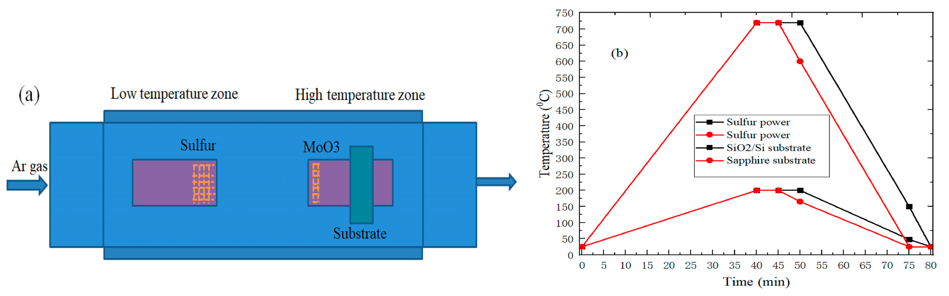
2. Experimental Methods

The specific experiment processes are as follows: single crystal sapphire substrate (C<0001>, 99.999%, and hexagonal lattice structure, 6Carbon Technology, Shenzhen, China), and silicon substrate with a thickness of 285 nm silicon dioxide (6Carbon Technology, Shenzhen, China) are selected in this experiment. Firstly, the SiO2/Si and sapphire substrates were sequentially placed in acetone, deionized water, absolute ethanol, and deionized water for ultrasonic cleaning for 10, 5, 10, and 5 min, respectively, and dried with nitrogen gas gun [17,18]. Then, 100 mg sulfur powder (99.5%, Alfa Aesar, Shanghai, China) and 2 mg molybdenum trioxide powder (MoO3, 99.95%, Alfa Aesar, Shanghai, China) were separately weighed using an electronic analytical balance and each placed into two different quartz boats. The quartz boat containing sulfur powder was placed in the upstream low-temperature zone center of the tube furnace. Subsequently, substrate was placed, face-down, at 5 cm downstream from the MoO3 powder for, and then the quartz boat with face-down substrate and MoO3 powder was placed in the downstream high-temperature zone center of the tube furnace. The specific location of the experimental material is shown in Figure 1a. Afterwards, high-purity argon gas (99.999%) with a flow rate of 200 sccm was introduced into the quartz tube for 10 min to remove the air of the tube furnace [19]. Figure 1b shows the reaction temperature change, and the temperature in the low-temperature zone was set to 200 °C, and the heating rate was 4.38 °C/min. At the same time, the temperature in the high-temperature zone was set to 720 °C, and the heating rate was 17.5 °C/min. The growth time of sapphire and SiO2/Si substrate were maintained for 5 and 10 min under the growth temperature of 720 °C, respectively. Finally, the temperature of the tube furnace was cooled to room temperature naturally after the growth reaction was complete.
Different layer numbers of MoS2 on SiO2/Si and sapphire substrates were systematically characterized by OM, AFM, and Raman and PL spectroscopy [20]. The test characterization experiment of MoS2 was the high-resolution Raman spectroscopy of LabRam HR Evolution model (HORIBA Jobin Yvon, Paris, France) using a high-definition color camera, which can achieve all functions of a standard microscope. Under the premise of maintaining constant room temperature, the specific test conditions of Raman spectroscopy are as follows: laser wavelength of 532 and 633 nm; spot diameter of 1 μm; spectral resolution ≤ 0.65 cm−1; scan time of 5 s; and the accumulation number of 3 s. In addition, the AFM (Dimension Icon, NanoScope8.10, Beijing, China) with 2% scanning accuracy error was also used to explore the size, thickness, surface morphology, and properties of MoS2 grown on sapphire and SiO2/Si substrates [21].

3. Results and Discussion

3.1. Monolayer MoS2 on Sapphire Substrate and SiO2/Si Substrates

The SiO2/Si and sapphire substrates are suitable substrate materials for growing high-quality, large-area, uniform triangles of MoS2. In addition, the surface topography of MoS2 on the SiO2/Si and sapphire substrates can easily be observed by optical microscopy.
Raman spectroscopy can determine the layer number, layer stress, and doping level of MoS2, so the Raman spectrum can further help us to master the structural characteristics of MoS2. In Figure 2a, the Raman spectrum peak of monolayer MoS2 on a sapphire substrate is much weaker than that on the SiO2/Si substrate; the reason is that the sapphire substrate is transparent, and the Raman spectrum collects the reflected light from MoS2. It can be seen from Figure 2b that the PL spectrum of MoS2+sapphire is formed by the combination between monolayer MoS2 and sapphire substrate. The B peak corresponds to the direct jump of B exciter due to the valence band splitting at the K point in the Brillouin zone [22]. The B peak of MoS2+sapphire PL spectrum is much stronger than that of a pure sapphire substrate, which can be explained by the strong coupling between MoS2 and sapphire substrate, and the efficient energy transfer occurs in MoS2 samples on the sapphire substrate.

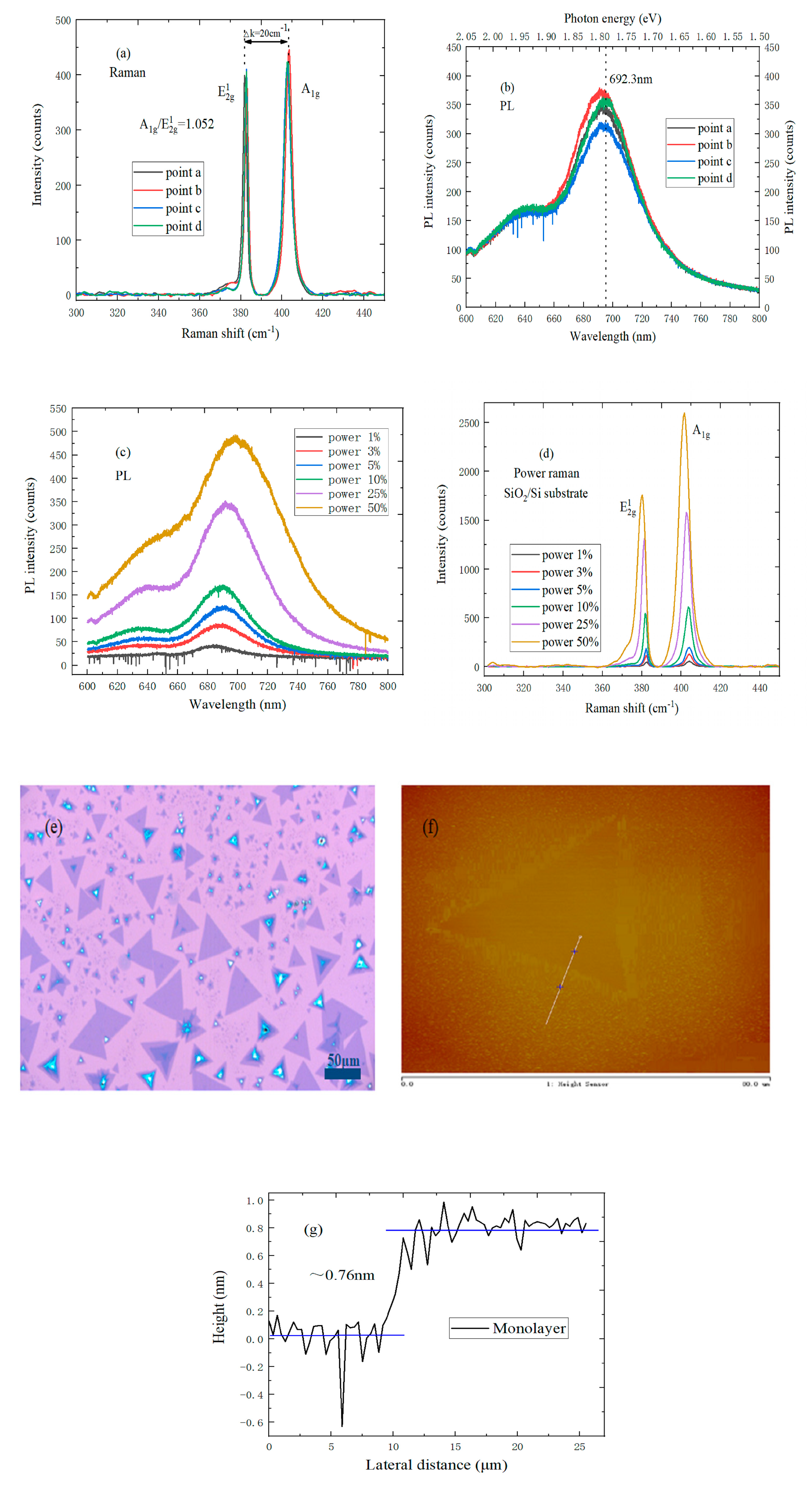
3.2. Characterization of Monolayer MoS2 on SiO2/Si Substrate

In Figure 3a, the Gauss–Lorentz function is used to fit the Raman spectrum. There are two characteristic peaks in the Raman spectrum, the E12g and A1g peak, and the peak shift difference between E12g and A1g was 20 cm−1, and the ratio A1g/E12g = 1.052 ≈ 1, which can help in establishing that the MoS2 sample is monolayer.
There exist I and B exciton peaks on a SiO2/Si substrate, and the PL spectrum of monolayer MoS2 is dominated by free exciton transition luminescence at room temperature.
E = h × H = h k × c λ = 1243 λ
The Planck constant, wavelength, energy, constant, and light speed are respectively represented by the symbols h, λ, E, k, and c in Equation (1), and the units of h, λ, E, k, and c are J.s, nm, eV, J/eV, and nm/s, respectively. According to the conversion relationship between photon energy and laser wavelength [23], it can be found from Figure 3b that the strongest photoluminescence peak is at 692.3 nm, and the corresponding photon energy is about 1.8 eV. In addition, a B exciton peak exists near 2.0 eV due to energy band splitting, which is the same as the reported band gap of monolayer MoS2 [24]. In Figure 3c, the I exciton peak is dominant in PL spectrum intensity under the low excitation power. Meanwhile, the B exciton peak position and I exciton peak shape did not change much when the excitation power increased, but the shape of the B exciton peak changed significantly. Moreover, the relative position between the I exciton peak and B exciton peak was redshifted to some extent when the laser power increases, which can be explained by the introduction of n-type doping MoS2 on the SiO2/Si substrate. Figure 3d shows the Raman spectrum of monolayer MoS2 with different laser power. When the laser power was increased, the Raman spectrum peak intensity increased, and the E12g characteristic peak was blueshifted. The reason is that the MoS2 grown on the SiO2/Si substrate is an n-type doped semiconductor [25]. Figure 3e shows the uniform triangular monolayer MoS2 with a side length of 50 μm on the SiO2/Si substrate, which is much larger than monolayer MoS2 obtained by the mechanical peeling method [26]. In addition, the surface color of monolayer MoS2 is uniform, which is in sharp contrast with the color of the SiO2/Si substrate, so it can be determined that the MoS2 sample is monolayer. It also can be seen from Figure 3f,g that triangular MoS2 has a very uniform color, and the thickness is 0.76 ± 0.015 nm, which can also indicate that the grown MoS2 is monolayer.

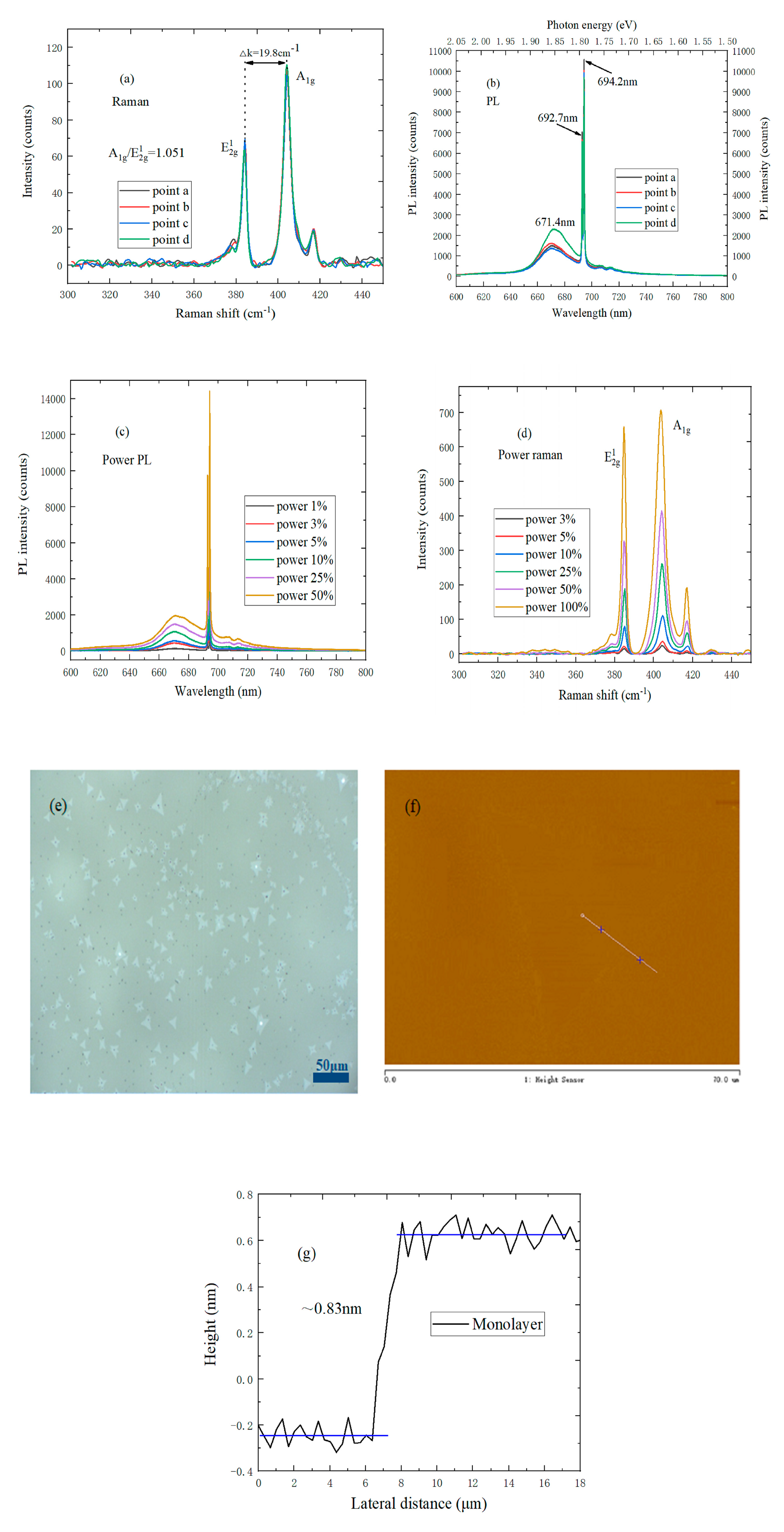
3.3. Characterization of Monolayer MoS2 on Sapphire Substrate

In Figure 4a, the characteristic Raman peak position difference of monolayer MoS2 on a sapphire substrate is 19.8 cm−1, and A1g/E12g ≈ 1.051, which is basically the same as the Raman spectrum of monolayer MoS2 on a SiO2/Si substrate. As shown in Figure 4b, the B peak of the PL spectrum on the sapphire substrate has a blueshift of 56 meV compared to the n-type doped monolayer MoS2 on the SiO2/Si substrate. The reason is that the sapphire substrate does not introduce any doping into the MoS2, and the optical transition process was dominated by neutral exciton radiation. It can be found by observing Figure 4c that the photoluminescence peaks at 671 and 693 nm correspond to the B exciton peak and the sapphire substrate, respectively, and the PL intensity of monolayer MoS2 is proportional to the laser power, which indicates that the monolayer MoS2 on the sapphire substrate did not undergo saturation absorption. This is because there was no charged impurity on the surface of the sapphire substrate, so no doping was introduced into MoS2 [27,28]. Figure 4d shows the Raman spectrum of monolayer MoS2 on the sapphire substrate at different laser powers. The Raman spectrum peak intensity increases with laser power increases. Unlike the SiO2/Si substrate, the characteristic E12g peak does not exist in the blueshift since the sapphire substrate does not introduce any doping into the monolayer MoS2. In Figure 4e, the shape of monolayer MoS2 is triangular, and the size can be up to 30 μm. As shown in Figure 4f,g, the triangular MoS2 has uniform color, and the thickness of MoS2 is about 0.83 ± 0.017 nm, which indicates that the MoS2 sample is monolayer.

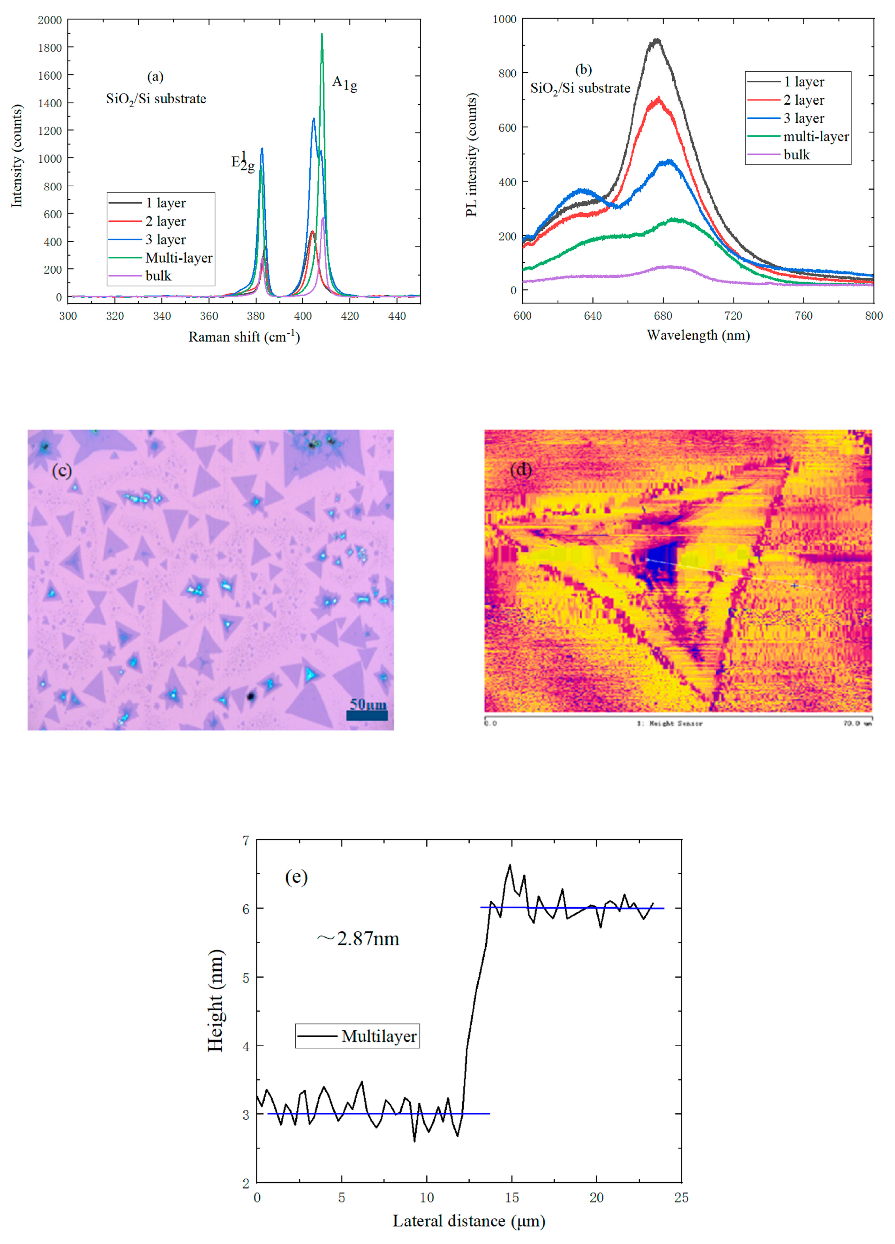
3.4. Characterization of Different Layers of MoS2 on SiO2/Si Substrate

In order to analyze the lattice vibration modes, the Raman and PL spectrums of different layer MoS2 on the SiO2/Si and sapphire substrates were tested. In Figure 5a, the greater the layer number of MoS2, the brighter the color under the microscope, which indicates the presence of MoS2 with different layer numbers on the surface of the SiO2/Si substrate. From bulk to monolayer samples, MoS2 had two distinct characteristic peaks in the range of 300~450 cm−1: E12g and A1g peaks. The E12g peak corresponds to the vibration of Mo atom and S atom parallel to the layer, and the A1g peak corresponds to the vibration of S atom perpendicular to the layer. The E12g peak with in-plane vibration mode is redshifted when the number of layers of MoS2 increase. This is because the short-range van der Waals force is stronger than dielectric shielding of the long-range Coulomb interaction. Meanwhile, the A1g peak of out-of-plane vibration mode has blueshifted with the gradual decrease of van der Waals force [29]. It can be seen from Figure 5b that the photoluminescence of the 2-layer and 3-layer MoS2 can also be observed due to the interaction between the layers. The B peak and I peak of monolayer MoS2 are respectively located at 627 and 677 nm. The I peak of the PL spectrum corresponds to direct exciton transition at the K point of Brillouin zone, and the B peak corresponds to the B exciton peak direct transition, which is caused by the valence band splitting. The I peak exists and is slightly redshifted when the MoS2 layer number increases; this is because the electron band gap at the K point of the Brillouin zone decreases, and the increase in interlayer van der Waals forces. In addition, the PL intensity increases gradually when the MoS2 layer number decreases. Therefore, monolayer MoS2 has the highest PL quantum yield, which is related to the phonon-dependent carrier band relaxation [30].
η L u m K r a d / ( K r a d + K d e f e c t + K r e l a x )
The K r a d , K d e f e c t , and K r e l a x in Formula (2) refer to the radiation recombination rate, defect trapping rate, and carrier relaxation rate, respectively. The K r e l a x decreases as the indirect band gap width increases, which leads to an increase in the luminescence intensity and an essential change in the electronic structure of MoS2. Therefore, the monolayer MoS2 is K r e l a x = 0 . Figure 5c shows the optical micrograph of MoS2 with different layer numbers on the SiO2/Si substrate. The triangular shape of MoS2 has a distinct color contrast with the SiO2/Si substrate, and the size can be up to 30 μm. As shown in Figure 5d,e, the color of triangular MoS2 is not uniform, and the thickness of middle MoS2 is about 2.87 ± 0.057 nm, which indicates that the grown MoS2 is a multilayer.

3.5. Characterization of Different Layers MoS2 on Sapphire Substrate

In Figure 6a, the interlayer van der Waals force increase gradually with the increase of MoS2 layer number, which would result in an increase of the mechanical constant and redshifting of the A1g peak. Meanwhile, the the characteristic E12g peak redshifts to some extent; this is because long-range Coulomb interactions play a more prominent role in the control of the atomic vibration when the MoS2 layer numbers increase. Therefore, the frequency shift difference between the characteristic E12g and A1g peaks on the sapphire substrate increase monotonically with the increase of MoS2 layer number. It is not difficult to find, when observing Figure 6b, that the bulk of the MoS2 on the sapphire substrate does not exist in the PL peak. When the MoS2 layer number decreases, MoS2 change from an indirect band gap to direct band gap, and the PL intensity increases gradually, so the PL intensity of monolayer MoS2 can be up to its maximum value. The B peak of monolayer MoS2 exists in the blueshift region, slightly, due to the annihilation of the phonon-assisted decay channel. The 1- and 2-layer MoS2 on the sapphire substrate has a higher PL peak intensity than that of 1- and 2-layer MoS2 on the SiO2/Si substrate. The reason is that the relative dielectric constant of the sapphire substrate is higher than that of the SiO2/Si substrate, which would result in the higher dielectric shielding effect. Figure 6c shows the optical micrograph of MoS2 with different layers on the sapphire substrate, where the size of MoS2 triangles are mostly 20 μm, and the surface of MoS2 sample is relatively clean and uniform, which is in sharp contrast with the sapphire substrate. As shown in Figure 6d,e, the color and thicknesses of triangular MoS2 are not uniform, and the middle thickness of MoS2 is about 2.93 ± 0.059 nm, which indicates that the MoS2 sample is multilayered.

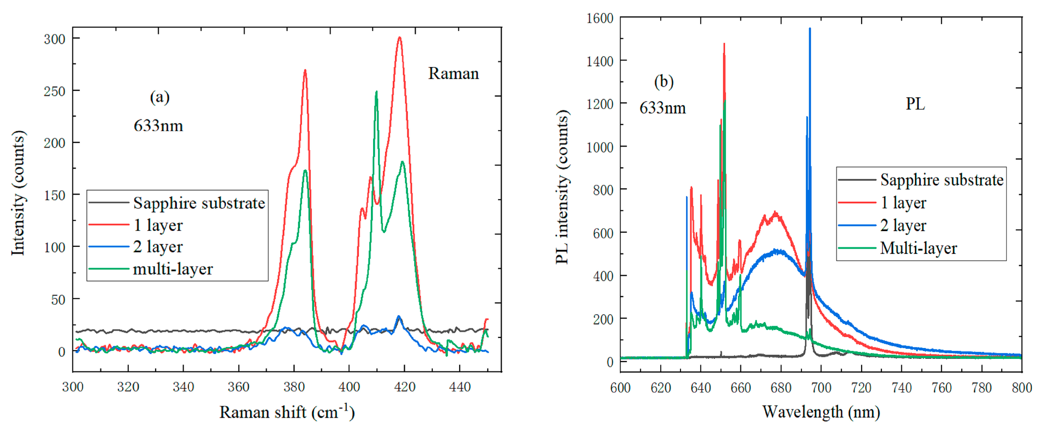
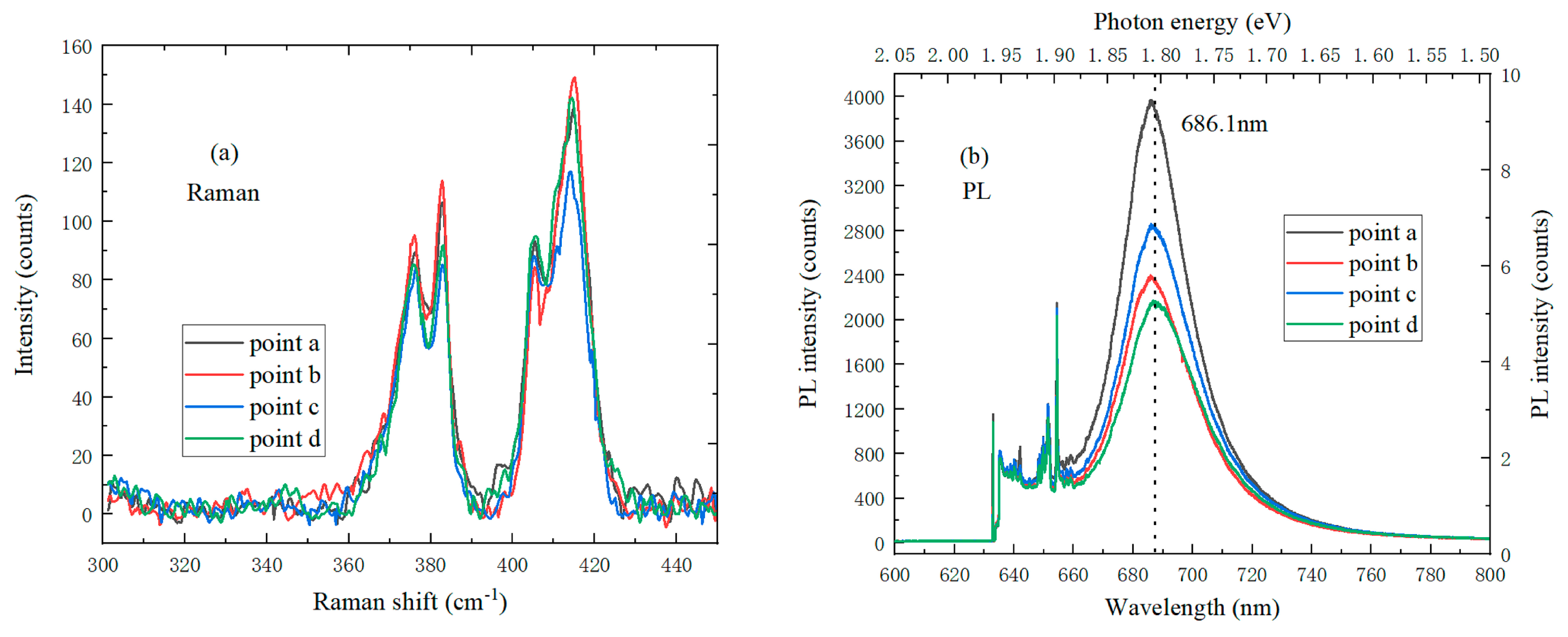
3.6. Characterization of MoS2 with Different Layers on Sapphire Substrate Under the 633 nm Laser Wavelength

In Figure 7a, the Raman spectrum of MoS2 with different layers on the sapphire substrate under the 633 nm laser wavelength, and the peak position of the MoS2 Raman spectrum are closely related to its thickness. Due to the increase in van der Waals forces, the characteristic E12g peak blueshifted while the characteristic A1g peak redshifted when the MoS2 layer number increased. It was possible to determine the layer number of MoS2 according to the wavenumber difference of A1g − E12g. Due to the very small local field effect, monolayer MoS2 had the strongest PL intensity. As shown in Figure 7b, the luminescence quantum efficiency of monolayer MoS2 was much higher than that of multilayer and bulk MoS2. The reason the PL intensity increases with decreasing MoS2 layer number is that the decrease of K r e l a x and the luminescence resonance state can match the direct exciton transfer. The PL phenomenon of monolayer MoS2 is an inherent property which is not caused by external disturbances.

3.7. Characterization of Monolayer MoS2 on SiO2/Si Substrate Under the 633 nm Laser Wavelength

The Raman spectrum of monolayer MoS2 on the SiO2/Si substrate was also tested under 633 nm laser wavelength, and the spectrum curve was fitted using the Gauss–Lorentz function, as shown in Figure 8a. The peak difference of monolayer MoS2 between the characteristic E12g and A1g peaks was 20 cm−1, which preliminarily established that MoS2 was monolayer. It can be seen from Figure 8b that the PL spectrum has its strongest peak intensity at 686.1 nm, and the corresponding photon energy is 1.81 eV, which is consistent with the absorption transition peak of I excitation. Compared to the PL spectrum of monolayer MoS2 at 532 nm, it can be found that the position of the I exciton peak has a blueshift of 16 meV, and the PL intensity of monolayer MoS2 increases when the laser wavelength transforms from 532 to 633 nm. The reason is due to the transition of the upper energy level of spin cleavage valence band to the conduction band.

4. Conclusions

In this paper, large size and high-quality MoS2 layers were grown on the SiO2/Si and sapphire substrates by APCVD. The optical properties of MoS2 on the SiO2/Si and sapphire substrates were researched systematically by atomic force microscopy, optical microscopy, and Raman and photoluminescence spectroscopy under different laser light wavelengths and powers. The peak shift between characteristic A1g and E12g peaks increased monotonously, and the I peak of the PL spectrum on the SiO2/Si substrate redshifted slightly when the layer number of MoS2 was increased, which can help to obtain the layer number and peak position of MoS2. In addition, the effects of layer number and external substrate environment on the optical properties of MoS2 were also studied systematically. The difference from monolayer MoS2 on the SiO2/Si substrate is that the B peak of the PL spectrum had a blueshift of 56 meV and the characteristic E12g peak of the Raman spectrum had no blueshift. The 1- and 2-layer MoS2 on the sapphire substrate has a higher PL peak intensity than that of the SiO2/Si substrate. When the laser wavelength transforms from 532 to 633 nm, the position of the I exciton peak had a blueshift of 16 meV, and the PL intensity of monolayer MoS2 on a SiO2/Si substrate increased. The optical properties of MoS2 can be obtained, which can pave the way for the fabrication of optoelectronic devices.

Author Contributions

Conceptualization and writing—original draft preparation, T.H. and X.Y.; methodology, S.W. and S.C.; validation, T.H., M.C. and K.Y.; writing—review and editing, H.L. and W.L.; funding acquisition, H.L.

Funding

This research was funded by the National Natural Science Foundation of China (Grant No. U1866212), the Foundation for Fundamental Research of China (Grant No. JSZL2016110B003), the Major Fundamental Research Program of Shaanxi (Grant No. 2017ZDJC-26), innovation Foundation of Radiation Application (Grant No.KFZC2018040206), the Fundamental Research Funds for the Central Universities (Grant No. 20101196741) and supported by the Shanghai Aerospace Science and Technology Innovation Fund, the Fundamental Research Funds for the Central Universities, and the Innovation Fund of Xidian University.

Conflicts of Interest

The authors declare no conflict of interest.

References

  1. Jeong, H.; Kim, U.; Kim, H.; Han, G.; Lee, H.; Kim, M.; Jin, Y.; Ly, T.; Lee, S.; Roh, Y. Optical Gain in MoS2 via Coupling with Nanostructured Substrate: Fabry-Perot Interference and Plasmonic Excitation. ACS Nano 2016, 10, 8192. [Google Scholar] [CrossRef]
  2. Kong, L.-J.; Liu, G.-H.; Qiang, L. Electronic and optical properties of O-doped monolayer MoS2. Comput. Mater. Sci. 2016, 111, 416–423. [Google Scholar] [CrossRef]
  3. Li, Z.; Li, Y.; Han, T.; Wang, X.; Yu, Y.; Tay, B.; Liu, Z.; Fang, Z. Tailoring MoS2 exciton–plasmon interaction by optical spin–orbit coupling. ACS Nano 2016, 11, 1165–1171. [Google Scholar] [CrossRef]
  4. Li, D.; Xiao, Z.; Mu, S.; Wang, F.; Liu, Y.; Song, J.; Huang, X.; Jiang, L.; Xiao, J.; Liu, L. A facile space-confined solid-phase sulfurization strategy for growth of high-quality ultrathin molybdenum disulfide single crystals. Nano Lett. 2018, 18, 2021–2032. [Google Scholar] [CrossRef] [PubMed]
  5. Michail, A.; Delikoukos, N.; Parthenios, J.; Galiotis, C.; Papagelis, K. Optical detection of strain and doping inhomogeneities in single layer MoS2. Appl. Phys. Lett. 2016, 108, 173102. [Google Scholar] [CrossRef]
  6. Das, S.; Chen, H.Y.; Penumatcha, A.V.; Appenzeller, J. High Performance Multilayer MoS2 Transistors with Scandium Contacts. Nano Lett. 2013, 13, 100. [Google Scholar] [CrossRef]
  7. Yin, Z.; Li, H.; Li, H.; Jiang, L.; Shi, Y.; Sun, Y.; Lu, G.; Zhang, Q.; Chen, X.; Zhang, H. Single-layer MoS2 phototransistors. ACS Nano 2011, 6, 74–80. [Google Scholar] [CrossRef] [PubMed]
  8. Zobel, A.; Boson, A.; Wilson, P.M.; Muratov, D.S.; Kuznetsov, D.V.; Sinitskii, A. Chemical vapour deposition and characterization of uniform bilayer and trilayer MoS 2 crystals. J. Mater. Chem. C 2016, 4, 11081–11087. [Google Scholar] [CrossRef]
  9. Anbazhagan, R.; Vadivelmurugan, A.; Tsai, H.-C.; Jeng, R.-J. Surface-enhanced Raman scattering of alkyne-conjugated MoS 2: A comparative study between metallic and semiconductor phases. J. Mater. Chem. C 2018, 6, 1071–1082. [Google Scholar] [CrossRef]
  10. Bertolazzi, S.; Krasnozhon, D.; Kis, A. Nonvolatile memory cells based on MoS2/graphene heterostructures. ACS Nano 2013, 7, 3246. [Google Scholar] [CrossRef]
  11. Jiang, L.; Lin, B.; Li, X.; Song, X.; Xia, H.; Li, L.; Zeng, H. Monolayer MoS2–graphene hybrid aerogels with controllable porosity for lithium-ion batteries with high reversible capacity. ACS Appl. Mater. Interfaces 2016, 8, 2680–2687. [Google Scholar] [CrossRef] [PubMed]
  12. Ning, F.; Wang, D.; Feng, Y.-X.; Tang, L.-M.; Zhang, Y.; Chen, K.-Q. Strong interfacial interaction and enhanced optical absorption in graphene/InAs and MoS2/InAs heterostructures. J. Mater. Chem. C 2017, 5, 9429–9438. [Google Scholar] [CrossRef]
  13. Sundaram, R.; Engel, M.; Lombardo, A.; Krupke, R.; Ferrari, A.; Avouris, P.; Steiner, M. Electroluminescence in single layer MoS2. Nano Lett. 2013, 13, 1416–1421. [Google Scholar] [CrossRef] [PubMed]
  14. Jia, G.Y.; Liu, Y.; Gong, J.Y.; Lei, D.Y.; Wang, D.L.; Huang, Z.X. Excitonic quantum confinement modified optical conductivity of monolayer and few-layered MoS2. J. Mater. Chem. C 2016, 4, 8822–8828. [Google Scholar] [CrossRef]
  15. Lopez-Sanchez, O.; Lembke, D.; Kayci, M.; Radenovic, A.; Kis, A. Ultrasensitive photodetectors based on monolayer MoS2. Nat. Nanotechnol. 2013, 8, 497. [Google Scholar] [CrossRef] [PubMed]
  16. Zhang, Y.; Xu, L.; Walker, W.R.; Tittle, C.M.; Backhouse, C.J.; Pope, M.A. Langmuir films and uniform, large area, transparent coatings of chemically exfoliated MoS2 single layers. J. Mater. Chem. C 2017, 5, 11275–11287. [Google Scholar] [CrossRef]
  17. Plechinger, G.; Mann, J.; Preciado, E.; Barroso, D.; Nguyen, A.; Eroms, J.; Schueller, C.; Bartels, L.; Korn, T. A direct comparison of CVD-grown and exfoliated MoS2 using optical spectroscopy. Semicond. Sci. Technol. 2014, 29, 064008. [Google Scholar] [CrossRef]
  18. Xu, W.; Li, S.; Zhou, S.; Lee, J.K.; Wang, S.; Sarwat, S.G.; Wang, X.; Bhaskaran, H.; Pasta, M.; Warner, J.H. Large dendritic monolayer MoS2 grown by atmospheric pressure chemical vapor deposition for electrocatalysis. ACS Appl. Mater. Interfaces 2018, 10, 4630–4639. [Google Scholar] [CrossRef]
  19. Li, Z.; Ye, R.; Feng, R.; Kang, Y.; Zhu, X.; Tour, J.M.; Fang, Z. Graphene quantum dots doping of MoS2 monolayers. Adv. Mater. 2015, 27, 5235–5240. [Google Scholar] [CrossRef] [PubMed]
  20. Fadil, D.; Hossain, R.F.; Saenz, G.A.; Kaul, A.B. On the chemically-assisted excitonic enhancement in environmentally-friendly solution dispersions of two-dimensional MoS2 and WS2. J. Mater. Chem. C 2017, 5, 5323–5333. [Google Scholar] [CrossRef]
  21. Rukelj, Z.; Štrkalj, A.; Despoja, V. Optical absorption and transmission in a molybdenum disulfide monolayer. Phys. Rev. B 2016, 94, 115428. [Google Scholar] [CrossRef]
  22. Choudhury, P.; Ravavarapu, L.; Dekle, R.; Chowdhury, S. Modulating Electronic and Optical Properties of Monolayer MoS2 Using Nonbonded Phthalocyanine Molecules. J. Phys. Chem. C 2017, 121, 2959–2967. [Google Scholar] [CrossRef]
  23. Qiu, D.; Lee, D.U.; Pak, S.W.; Kim, E.K. Structural and optical properties of MoS2 layers grown by successive two-step chemical vapor deposition method. Thin Solid Films 2015, 587, 47–51. [Google Scholar] [CrossRef]
  24. Chow, P.K.; Singh, E.; Viana, B.C.; Gao, J.; Luo, J.; Li, J.; Lin, Z.; Elías, A.L.; Shi, Y.; Wang, Z. Wetting of mono and few-layered WS2 and MoS2 films supported on Si/SiO2 substrates. Acs Nano 2015, 9, 3023–3031. [Google Scholar] [CrossRef] [PubMed]
  25. Late, D.; DJ Late, Y.-K.; Huang, B.; Liu, J.; Acharya, S.N.; Shirodkar, J.; Luo, A.; Yan, D.; Charles, U.V.; Waghmare, V.P. Sensing behavior of atomically thin-layered MoS2 transistors. ACS Nano 2013, 7, 4879. [Google Scholar] [CrossRef] [PubMed]
  26. Vikraman, D.; Akbar, K.; Hussain, S.; Yoo, G.; Jang, J.-Y.; Chun, S.-H.; Jung, J.; Park, H.J. Direct synthesis of thickness-tunable MoS2 quantum dot thin layers: Optical, structural and electrical properties and their application to hydrogen evolution. Nano Energy 2017, 35, 101–114. [Google Scholar] [CrossRef]
  27. Mak, K.F.; Lee, C.; Hone, J.; Shan, J.; Heinz, T.F. Atomically thin MoS2: A new direct-gap semiconductor. Phys. Rev. Lett. 2010, 105, 136805. [Google Scholar] [CrossRef]
  28. Chae, W.H.; Cain, J.D.; Hanson, E.D.; Murthy, A.A.; Dravid, V.P. Substrate-induced strain and charge doping in CVD-grown monolayer MoS2. Appl. Phys. Lett. 2017, 111, 143106. [Google Scholar] [CrossRef]
  29. Zafar, A.; Nan, H.; Zafar, Z.; Wu, Z.; Jiang, J.; You, Y.; Ni, Z. Probing the intrinsic optical quality of CVD grown MoS2. Nano Res. 2017, 10, 1608–1617. [Google Scholar] [CrossRef]
  30. Splendiani, A.; Sun, L.; Zhang, Y.; Li, T.; Kim, J.; Chim, C.Y.; Galli, G.; Wang, F. Emerging photoluminescence in monolayer MoS2. Nano Lett. 2010, 10, 1271–1275. [Google Scholar] [CrossRef]
Figure 1. (a) The schematic diagram of MoS2 growth; (b) The change curve of experimental temperature.
Nanomaterials 09 00740 g001
Figure 2. (a) Raman spectrum of monolayer MoS2 on SiO2/Si and sapphire substrates; (b) PL spectrum of MoS2+sapphire and sapphire substrate at the 532 nm laser wavelength.
Nanomaterials 09 00740 g002
Figure 3. (a) Raman spectrum of four different points in monolayer MoS2 on a SiO2/Si substrate; (b) PL spectrum of four different points in monolayer MoS2 on a SiO2/Si substrate; (c) PL spectrum of monolayer MoS2 on a SiO2/Si substrate with different laser power; (d) Raman spectrum of monolayer MoS2 on a SiO2/Si substrate with different laser power; (e) Optical micrograph of monolayer MoS2 on a SiO2/Si substrate; (f) AFM morphology of monolayer MoS2 on a SiO2/Si substrate; (g) Height profile of monolayer MoS2 on a SiO2/Si substrate.
Nanomaterials 09 00740 g003
Figure 4. (a) Raman spectrum of four different points in monolayer MoS2 on a sapphire substrate; (b) PL spectrum of four different points in monolayer MoS2 on a sapphire substrate; (c) PL spectrum of monolayer MoS2 on a sapphire substrate at different laser powers; (d) Raman spectrum of monolayer MoS2 on a sapphire substrate at different laser powers; (e) Optical micrograph of monolayer MoS2 on a sapphire substrate; (f) AFM morphology of monolayer MoS2 on a sapphire substrate; (g) Height profile of monolayer MoS2 on a sapphire substrate.
Nanomaterials 09 00740 g004
Figure 5. (a) Raman spectrum of MoS2 with different layers on a SiO2/Si substrate; (b) PL spectrum of MoS2 with different layers on a SiO2/Si substrate; (c) Optical micrograph of MoS2 with different layers on a SiO2/Si substrate; (d) AFM morphology of multilayer MoS2 on a SiO2/Si substrate; (e) Height profile of multilayer MoS2 on a SiO2/Si substrate.
Nanomaterials 09 00740 g005
Figure 6. (a) Raman spectrum of MoS2 with different layers on a sapphire substrate; (b) PL spectrum of MoS2 with different layers on a sapphire substrate; (c) Optical micrograph of MoS2 with different layers on a sapphire substrate; (d) AFM morphology of multilayer MoS2 on a sapphire substrate; (e) Height profile of multilayer MoS2 on a sapphire substrate.
Nanomaterials 09 00740 g006
Figure 7. (a) Raman spectrum of MoS2 with different layers on the sapphire substrate; (b) PL spectrum of MoS2 with different layer on the sapphire substrate under the laser wavelength of 633 nm.
Nanomaterials 09 00740 g007
Figure 8. Optical properties of monolayer MoS2 on a SiO2/Si substrate under the laser wavelength of 633 nm (a) Raman spectrum; (b) PL spectrum.
Nanomaterials 09 00740 g008

