Raman Study of Strain Relaxation from Grain Boundaries in Epitaxial Graphene Grown by Chemical Vapor Deposition on SiC

Abstract
:1. Introduction
2. Materials and Methods
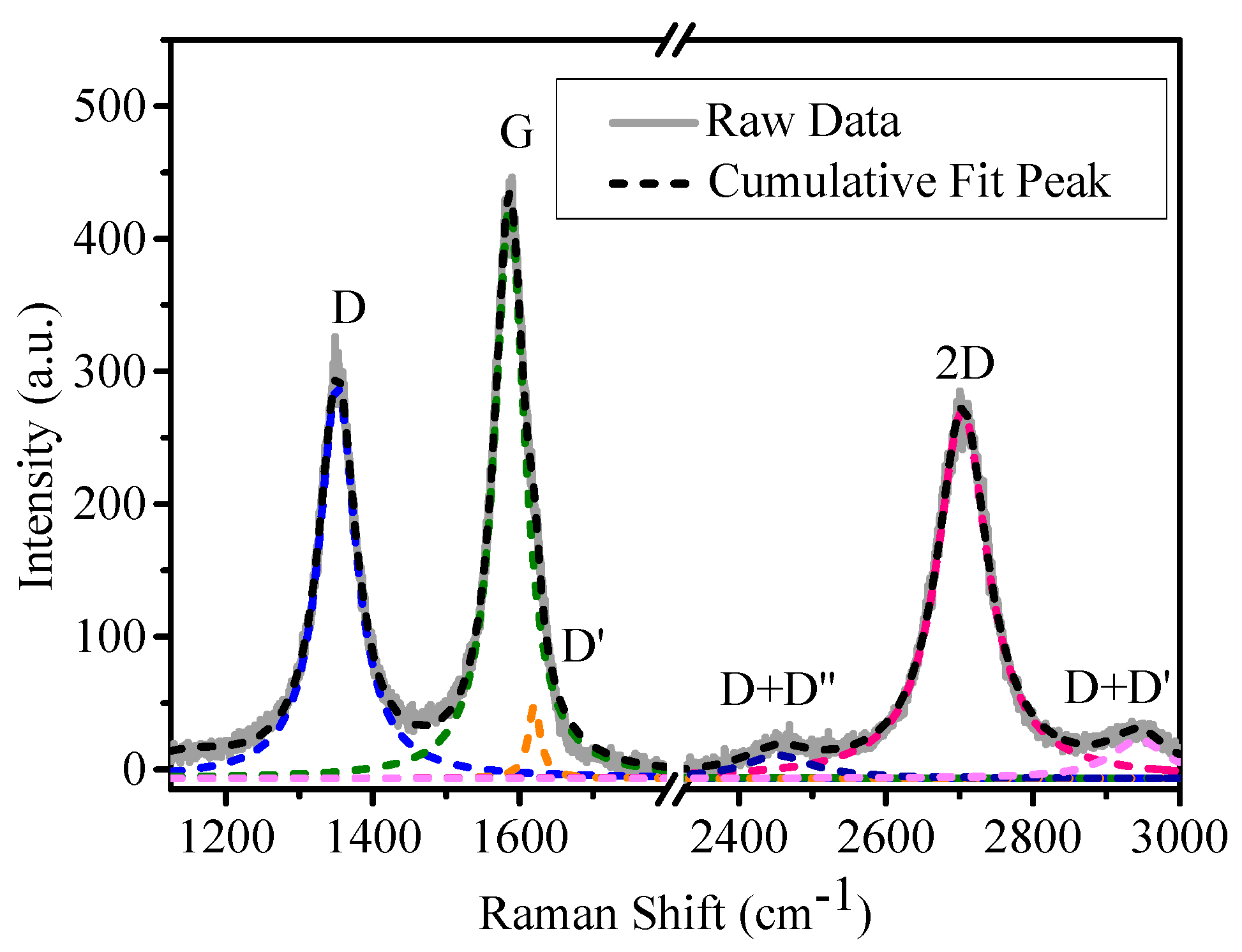
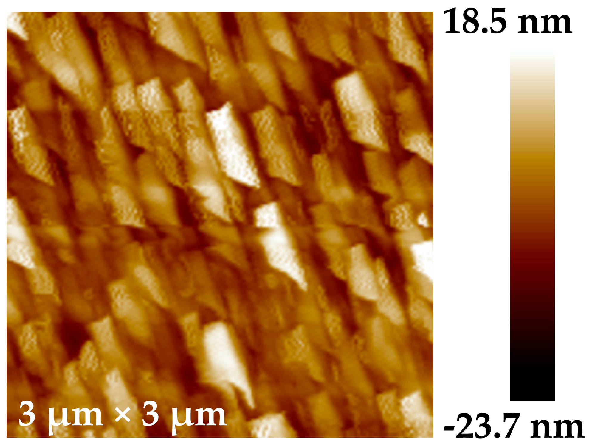
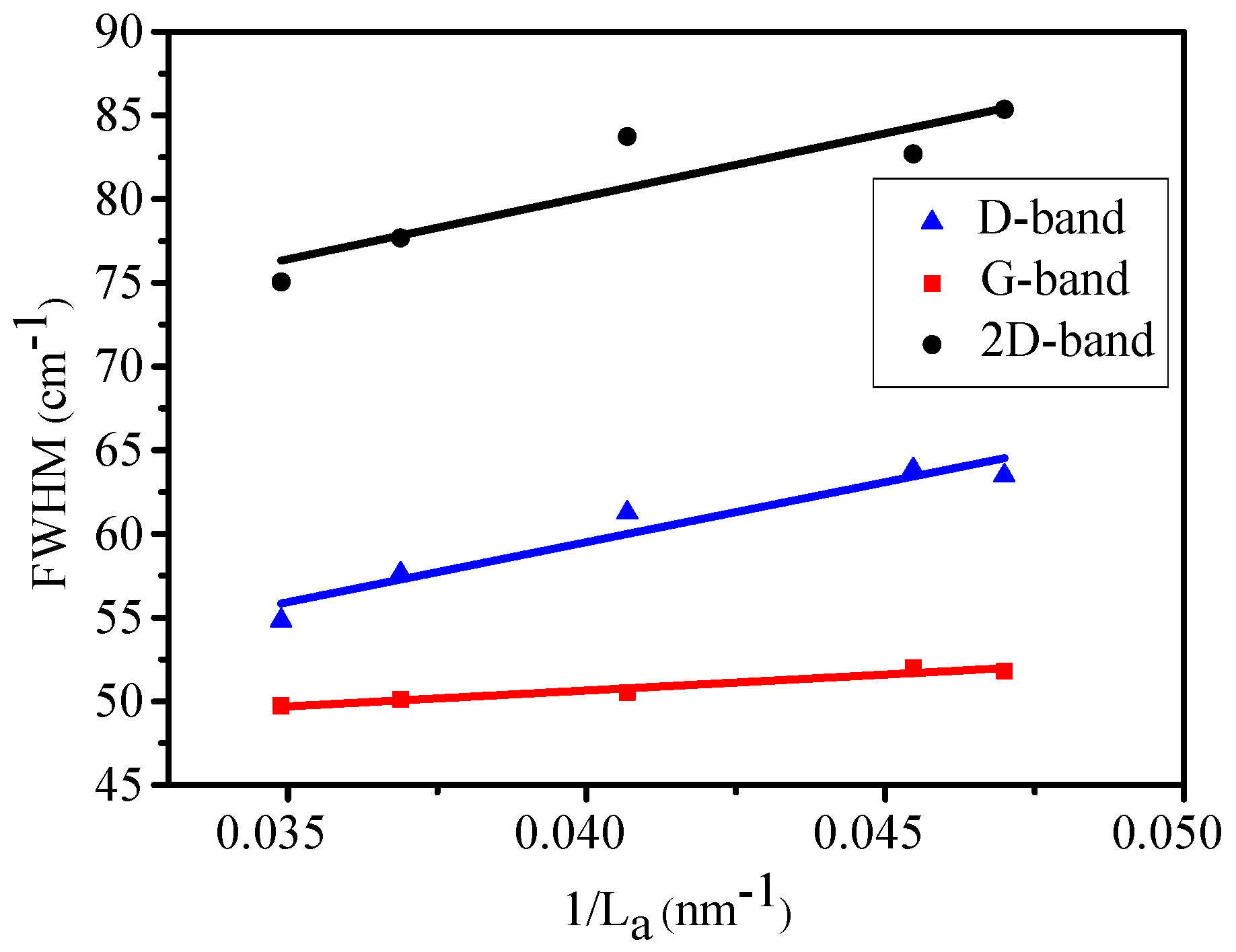
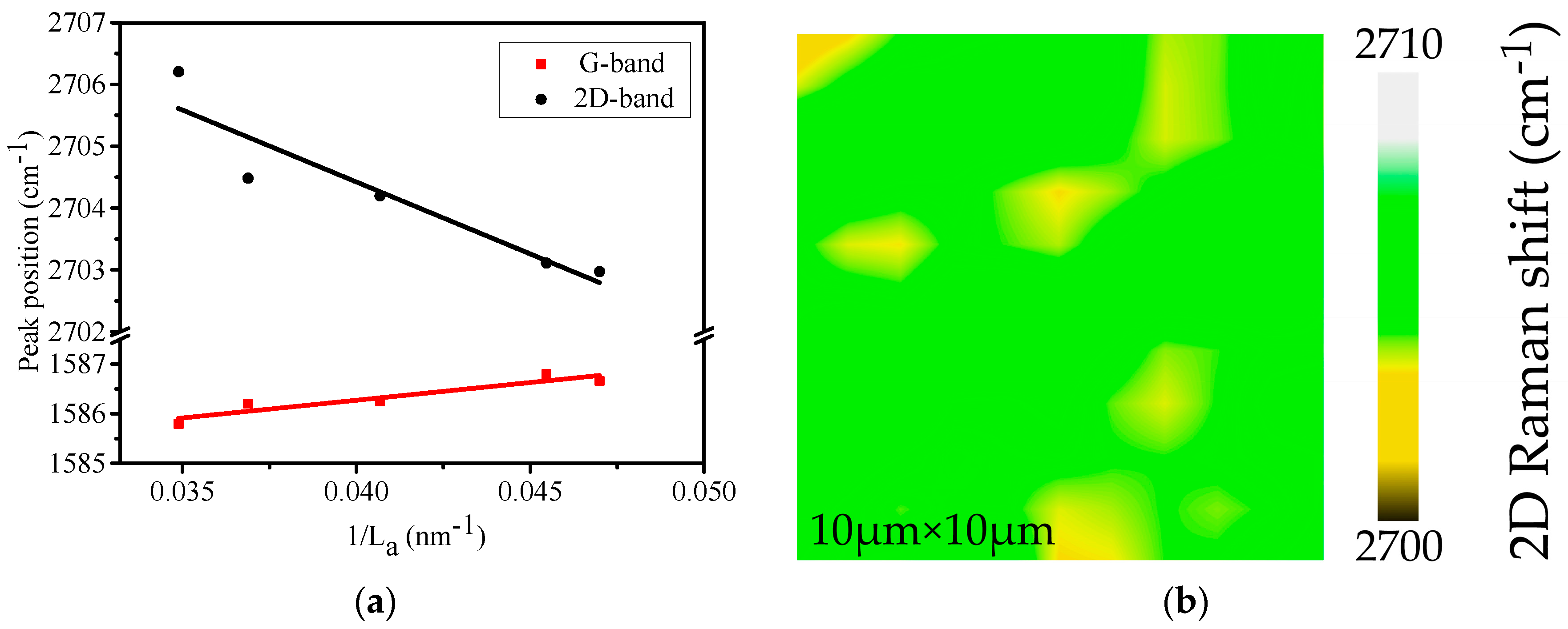
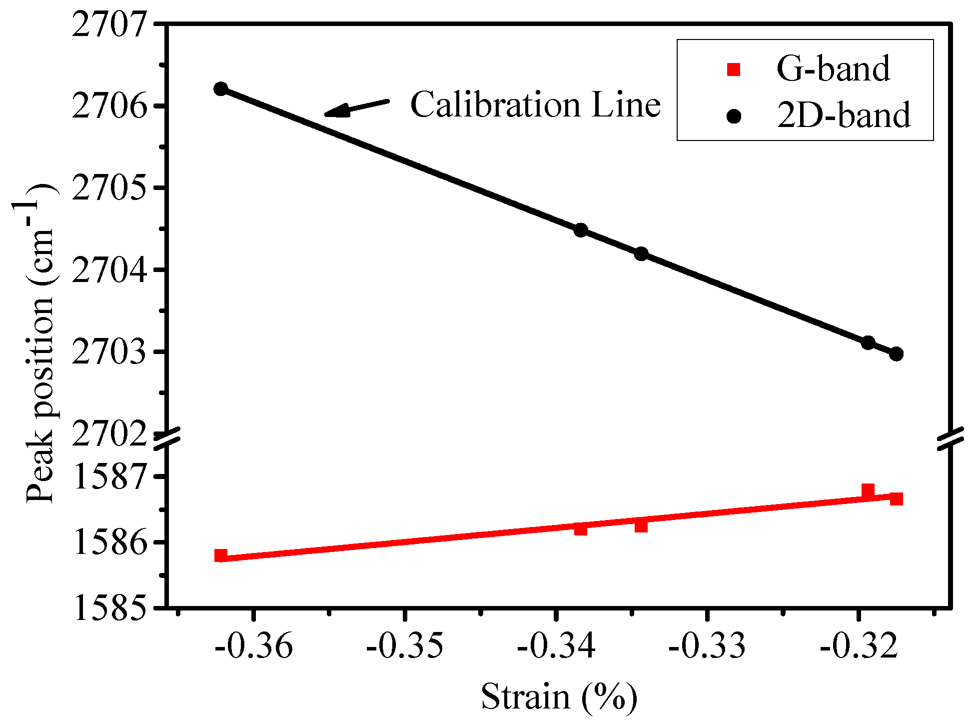
3. Results and Discussion
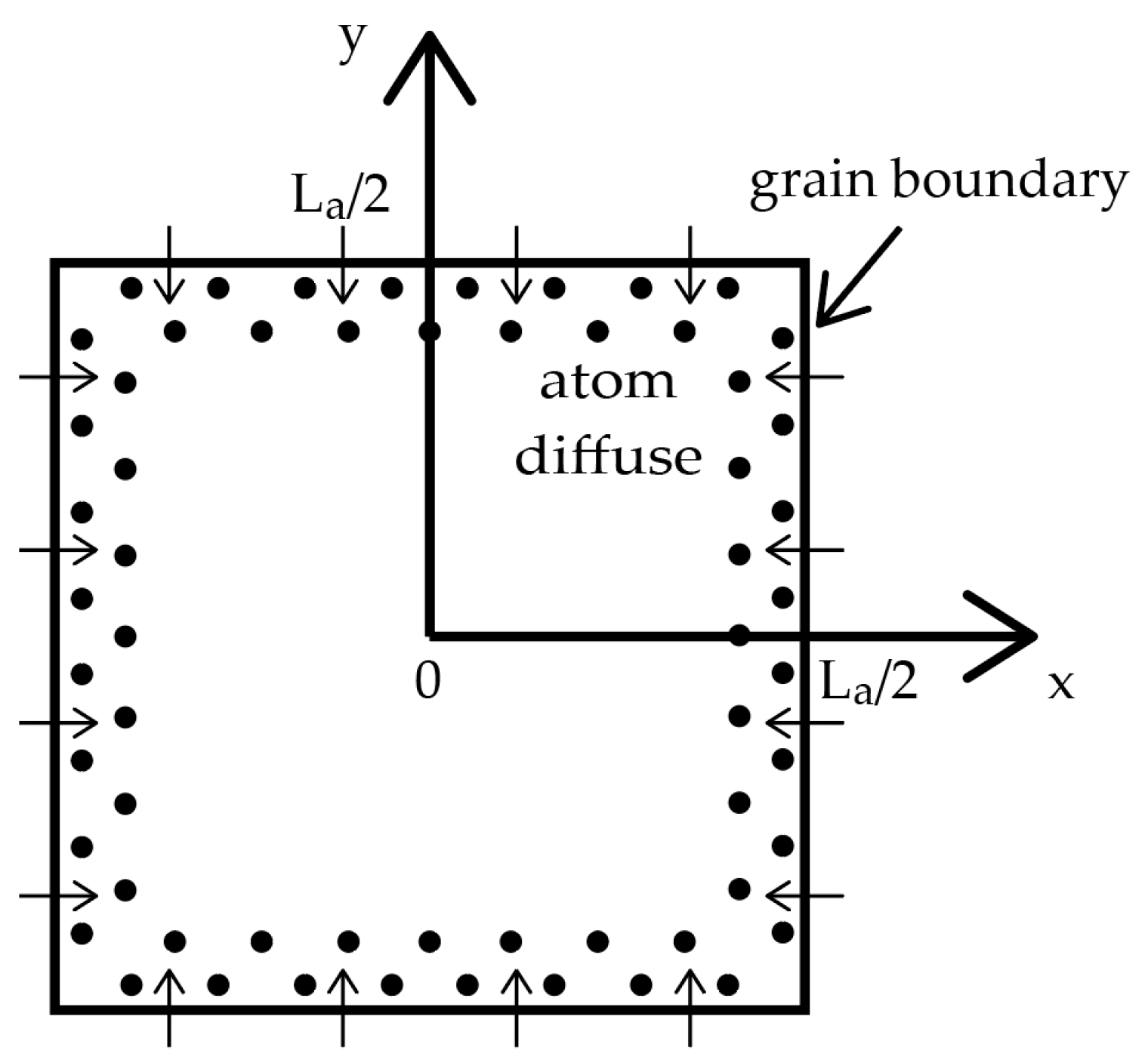
- (1)
- lattice diffusion directly into the grains and
- (2)
- much faster diffusion along the grain boundary.
4. Conclusions
Author Contributions
Funding
Conflicts of Interest
References
- Wu, J.-B.; Lin, M.-L.; Cong, X.; Liu, H.-N.; Tan, P.-H. Raman spectroscopy of graphene-based materials and its applications in related devices. Chem. Soc. Rev. 2018, 47, 1822–1873. [Google Scholar] [CrossRef] [PubMed]
- Bae, S.; Kim, H.; Lee, Y.; Xu, X.; Park, J.-S.; Zheng, Y.; Balakrishnan, J.; Lei, T.; Ri Kim, H.; Song, Y.I.; et al. Roll-to-Roll Production of 30-inch Graphene Films for Transparent Electrodes. Nat. Nanotechnol. 2010, 5, 574–578. [Google Scholar] [CrossRef] [PubMed]
- Wagner, S.; Dieing, T.; Centeno, A.; Zurutuza, A.; Smith, A.D.; Östling, M.; Kataria, S.; Lemme, M.C. Noninvasive Scanning Raman Spectroscopy and Tomography for Graphene Membrane Characterization. Nano Lett. 2017, 17, 1504–1511. [Google Scholar] [CrossRef] [PubMed]
- Xu, W.; Ling, X.; Xiao, J.; Dresselhaus, M.S.; Kong, J.; Xu, H.; Liu, Z.; Zhang, J. Surface enhanced Raman spectroscopy on a flat graphene surface. PNAS 2012, 109, 9281–9286. [Google Scholar] [CrossRef] [PubMed]
- Ling, X.; Xie, L.; Fang, Y.; Xu, H.; Zhang, H.; Kong, J.; Dresselhaus, M.S.; Zhang, J.; Liu, Z. Can Graphene be used as a Substrate for Raman Enhancement? Nano Lett. 2010, 10, 553–561. [Google Scholar] [CrossRef] [PubMed]
- Mueller, N.S.; Heeg, S.; Alvarez, M.P.; Kusch, P.; Wasserroth, S.; Clark, N.; Schedin, F.; Parthenios, J.; Papagelis, K.; Galiotis, C.; et al. Evaluating arbitrary strain configurations and doping in graphene with Raman spectroscopy. 2D Mater. 2018, 5, 015016. [Google Scholar] [CrossRef]
- Kim, S.; Ryu, S. Thickness-dependent native strain in graphene membranes visualized by Raman spectroscopy. Carbon 2016, 100, 283–290. [Google Scholar] [CrossRef]
- Strupinski, W.; Grodecki, K.; Wysmolek, A.; Stepniewski, R.; Szkopek, T.; Gaskell, P.E.; Grüneis, A.; Haberer, D.; Bozek, R.; Krupka, J.; et al. Graphene Epitaxy by Chemical Vapor Deposition on SiC. Nano Lett. 2011, 11, 1786–1791. [Google Scholar] [CrossRef] [PubMed]
- Lim, G.; Kihm, K.D.; Kim, H.G.; Lee, W.; Lee, W.; Pyun, K.R.; Cheon, S.; Lee, P.; Min, J.Y.; Ko, S.H. Enhanced Thermoelectric Conversion Efficiency of CVD Graphene with Reduced Grain Sizes. Nanomaterials 2018, 8, 557. [Google Scholar] [CrossRef] [PubMed]
- Chen, M.Q.; Quek, S.S.; Sha, Z.D.; Chiu, C.H.; Pei, Q.X.; Zhang, Y.W. Effects of grain size, temperature and strain rate on the mechanical properties of polycrystalline graphene—A molecular dynamics study. Carbon 2015, 85, 135–146. [Google Scholar] [CrossRef]
- Wang, B.; Puzyrev, Y.; Pantelides, S.T. Strain enhanced defect reactivity at grain boundaries in polycrystalline graphene. Carbon 2011, 49, 3983–3988. [Google Scholar] [CrossRef]
- Ren, Y.; Cao, G. Effect of geometrical defects on the tensile properties of graphene. Carbon 2016, 103, 125–133. [Google Scholar] [CrossRef]
- Xu, P.; Qi, D.; Schoelz, J.K.; Thompson, J.; Thibado, P.M.; Wheeler, V.D.; Nyakiti, L.O.; Myers-Ward, R.L.; Eddy, C.R., Jr.; Gaskill, D.K.; et al. Multilayer graphene, Moire’ patterns, grain boundaries and defects identified by scanning tunneling microscopy on the m-plane, non-polar surface of SiC. Carbon 2014, 80, 75–81. [Google Scholar] [CrossRef]
- Zhou, X.; Ji, S.H.; Chockalingam, S.P.; Hannon, J.B.; Tromp, R.M.; Heinz, T.F.; Pasupathy, A.N.; Ross, F.M. Electrical transport across grain boundaries in graphene monolayers on SiC(0001¯). 2D Mater. 2018, 5, 031004. [Google Scholar] [CrossRef]
- Tison, Y.; Lagoute, J.; Repain, V.; Chacon, C.; Girard, Y.; Joucken, F.; Sporken, R.; Gargiulo, F.; Yazyev, O.V.; Rousset, S. Grain Boundaries in Graphene on SiC(0001¯) Substrate. Nano Lett. 2014, 14, 6382–6386. [Google Scholar] [CrossRef] [PubMed]
- Bissett, M.A.; Izumida, W.; Saito, R.; Ago, H. Effect of Domain Boundaries on the Raman Spectra of Mechanically Strained Graphene. ACS Nano 2012, 6, 10229–10238. [Google Scholar] [CrossRef] [PubMed]
- Ferrante, C.; Virga, A.; Benfatto, L.; Martinati, M.; De Fazio, D.; Sassi, U.; Fasolato, C.; Ott, A.K.; Postorino, P.; Yoon, D.; et al. Raman spectroscopy of graphene under ultrafast laser excitation. Nat. Commun. 2018, 9, 308. [Google Scholar] [CrossRef] [PubMed]
- Krishna, R.; Wade, J.; Jones, A.N.; Lasithiotakis, M.; Mummery, P.M.; Marsden, B.J. An understanding of lattice strain, defects and disorder in nuclear graphite. Carbon 2017, 124, 314–333. [Google Scholar] [CrossRef]
- Lafont, F.; Ribeiro-Palau, R.; Kazazis, D.; Michon, A.; Couturaud, O.; Consejo, C.; Chassagne, T.; Zielinski, M.; Portail, M.; Jouault, B.; et al. Quantum Hall resistance standards from graphene grown by chemical vapour deposition on silicon carbide. Nat. Commun. 2015, 6, 6806. [Google Scholar] [CrossRef] [PubMed]
- Conrad, M.; Rault, J.; Utsumi, Y.; Garreau, Y.; Vlad, A.; Coati, A.; Rueff, J.-P.; Miceli, P.F.; Conrad, E.H. Structure and evolution of semiconducting buffer graphene grown on SiC(0001). Phys. Rev. B 2017, 96, 195304. [Google Scholar] [CrossRef]
- Fromm, F.; Oliveira, M.H., Jr.; Molina-S’anchez, A.; Hundhausen, M.; Lopes, J.M.J.; Riechert, H.; Wirtz, L.; Seyller, T. Contribution of the buffer layer to the Raman spectrum of epitaxial graphene on SiC(0001). New J. Phys. 2013, 15, 043031. [Google Scholar] [CrossRef]
- Magaud, L.; Hiebel, F.; Varchon, F.; Mallet, P.; Veuillen, J.-Y. Graphene on the C-terminated SiC (0001¯) surface: An ab initio study. Phys. Rev. B 2009, 79, 161405. [Google Scholar] [CrossRef]
- Hiebel, F.; Mallet, P.; Varchon, F.; Magaud, L.; Veuillen, J.-Y. Graphene-substrate interaction on 6H-SiC(0001¯): A scanning tunneling microscopy study. Phys. Rev. B 2008, 78, 153412. [Google Scholar] [CrossRef]
- Graf, D.; Molitor, F.; Ensslin, K.; Stampfer, C.; Jungen, A.; Hierold, C.; Wirtz, L. Spatially resolved Raman spectroscopy of single- and few-layer graphene. Nano Lett. 2007, 7, 238–242. [Google Scholar] [CrossRef] [PubMed]
- Röhrl, J.; Hundhausen, M.; Emtsev, K.V.; Seyller, T.; Graupner, R.; Ley, L. Raman spectra of epitaxial graphene on SiC(0001). Appl. Phys. Lett. 2008, 92, 201918. [Google Scholar] [CrossRef]
- Strudwick, A.J.; Creeth, G.L.; Johansson, N.A.B.; Marrows, C.H. Probing residual strain in epitaxial graphene layers on with Raman spectroscopy. Appl. Phys. Lett. 2011, 98, 051910. [Google Scholar] [CrossRef]
- Cançado, L.G.; Jorio, A.; Pimenta, M.A. Measuring the absolute Raman cross section of nanographites as a function of laser energy and crystallite size. Phys. Rev. B 2007, 76, 064304. [Google Scholar] [CrossRef]
- Lee, D.S.; Riedl, C.; Krauss, B.; von Klitzing, K.; Starke, U.; Smet, J.H. Raman Spectra of Epitaxial Graphene on SiC and of Epitaxial Graphene Transferred to SiO2. Nano Lett. 2008, 8, 4320–4325. [Google Scholar] [CrossRef] [PubMed]
- Robinson, J.A.; Puls, C.P.; Staley, N.E.; Stitt, J.P.; Fanton, M.A.; Emtsev, K.V.; Seyller, T.; Liu, Y. Raman Topography and Strain Uniformity of Large-Area Epitaxial Graphene. Nano Lett. 2009, 9, 964–968. [Google Scholar] [CrossRef] [PubMed]
- Ferrari, A.C.; Meyer, J.C.; Scardaci, V.; Casiraghi, C.; Lazzeri, M.; Mauri, F.; Piscanec, S.; Jiang, D.; Novoselov, K.S.; Roth, S.; et al. Raman Spectrum of Graphene and Graphene Layers. Phys. Rev. Lett. 2006, 97, 187401. [Google Scholar] [CrossRef] [PubMed]
- Wang, Y.Y.; Ni, Z.H.; Yu, T.; Wang, H.M.; Wu, Y.H.; Chen, W.; Wee, A.T.S.; Shen, Z.X. Raman studies of monolayer graphene: The substrate effect. J. Phys. Chem. C 2008, 112, 10637–10640. [Google Scholar] [CrossRef]
- Eckmann, A.; Felten, A.; Mishchenko, A.; Britnell, L.; Krupke, R.; Novoselov, K.S.; Casiraghi, C. Probing the Nature of Defects in Graphene by Raman Spectroscopy. Nano Lett. 2012, 12, 3925–3930. [Google Scholar] [CrossRef] [PubMed]
- Ferrari, A.C.; Basko, D.M. Raman spectroscopy as a versatile tool for studying the properties of graphene. Nat. Nanotechnol. 2013, 8, 235–246. [Google Scholar] [CrossRef] [PubMed]
- Eckmann, A.; Felten, A.; Verzhbitskiy, I.; Davey, R.; Casiraghi, C. Raman study on defective graphene: Effect of the excitation energy, type, and amount of defects. Phys. Rev. B 2013, 88, 035426. [Google Scholar] [CrossRef]
- Vantasin, S.; Tanaka, Y.; Uemura, S.; Suzuki, T.; Kutsuma, Y.; Doujima, D.; Kaneko, T.; Ozaki, Y. Characterization of SiC-grown epitaxial graphene microislands using tip-enhanced Raman spectroscopy. Phys. Chem. Chem. Phys. 2015, 17, 28993–28999. [Google Scholar] [CrossRef] [PubMed]
- Das, A.; Pisana, S.; Chakraborty, B.; Piscanec, S.; Saha, S.K.; Waghmare, U.V.; Novoselov, K.S.; Krishnamurthy, H.R.; Geim, A.K.; Ferrari, A.C.; et al. Monitoring dopants by Raman scattering in an electrochemically top-gated graphene transistor. Nat. Nanotechnol. 2008, 3, 210–215. [Google Scholar] [CrossRef] [PubMed]
- Mehrer, H. Diffusion in Solids; Springer: Berlin, Germany, 2007; pp. 553–582. [Google Scholar]
© 2019 by the authors. Licensee MDPI, Basel, Switzerland. This article is an open access article distributed under the terms and conditions of the Creative Commons Attribution (CC BY) license (http://creativecommons.org/licenses/by/4.0/).
Share and Cite
Chong, L.; Guo, H.; Zhang, Y.; Hu, Y.; Zhang, Y. Raman Study of Strain Relaxation from Grain Boundaries in Epitaxial Graphene Grown by Chemical Vapor Deposition on SiC. Nanomaterials 2019, 9, 372. https://doi.org/10.3390/nano9030372
Chong L, Guo H, Zhang Y, Hu Y, Zhang Y. Raman Study of Strain Relaxation from Grain Boundaries in Epitaxial Graphene Grown by Chemical Vapor Deposition on SiC. Nanomaterials. 2019; 9(3):372. https://doi.org/10.3390/nano9030372
Chicago/Turabian StyleChong, Laiyuan, Hui Guo, Yuming Zhang, Yanfei Hu, and Yimen Zhang. 2019. "Raman Study of Strain Relaxation from Grain Boundaries in Epitaxial Graphene Grown by Chemical Vapor Deposition on SiC" Nanomaterials 9, no. 3: 372. https://doi.org/10.3390/nano9030372
APA StyleChong, L., Guo, H., Zhang, Y., Hu, Y., & Zhang, Y. (2019). Raman Study of Strain Relaxation from Grain Boundaries in Epitaxial Graphene Grown by Chemical Vapor Deposition on SiC. Nanomaterials, 9(3), 372. https://doi.org/10.3390/nano9030372