Nanostructured Perovskite Solar Cells

 , , , and
Abstract

1. Introduction
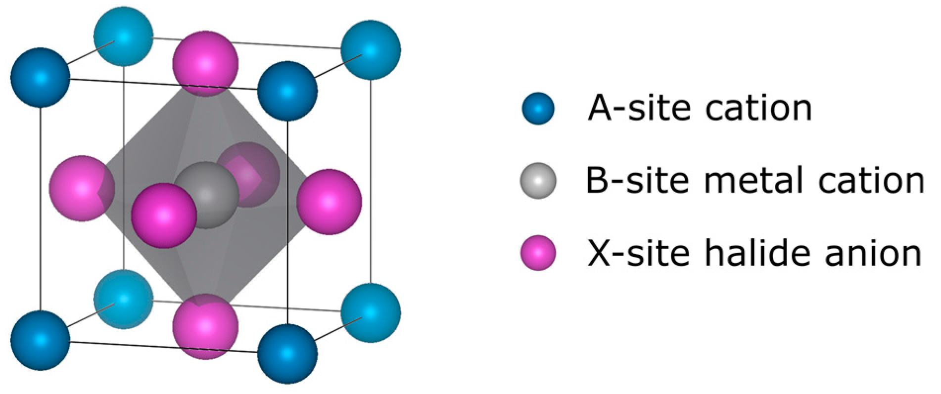
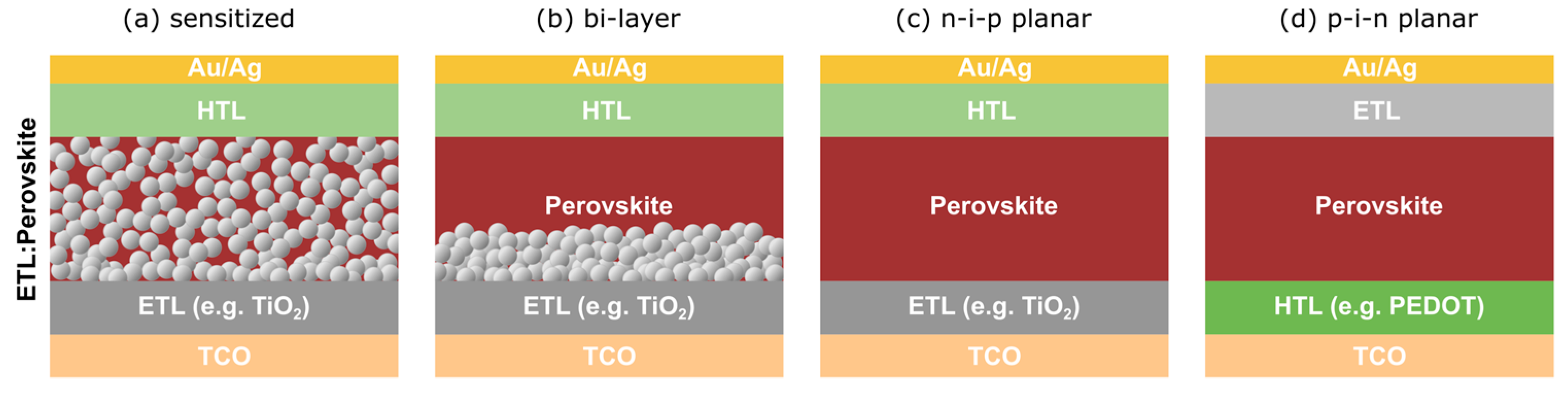
2. Overview of Bulk Perovskite Solar Cells
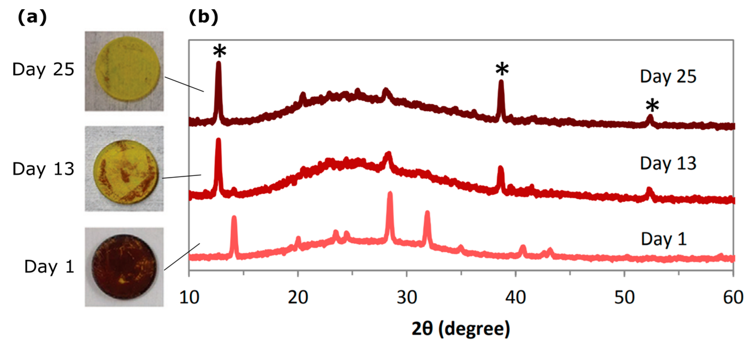
2.1. Stability of Perovskite Solar Cells
2.2. Toxicity of Perovskite Solar Cells
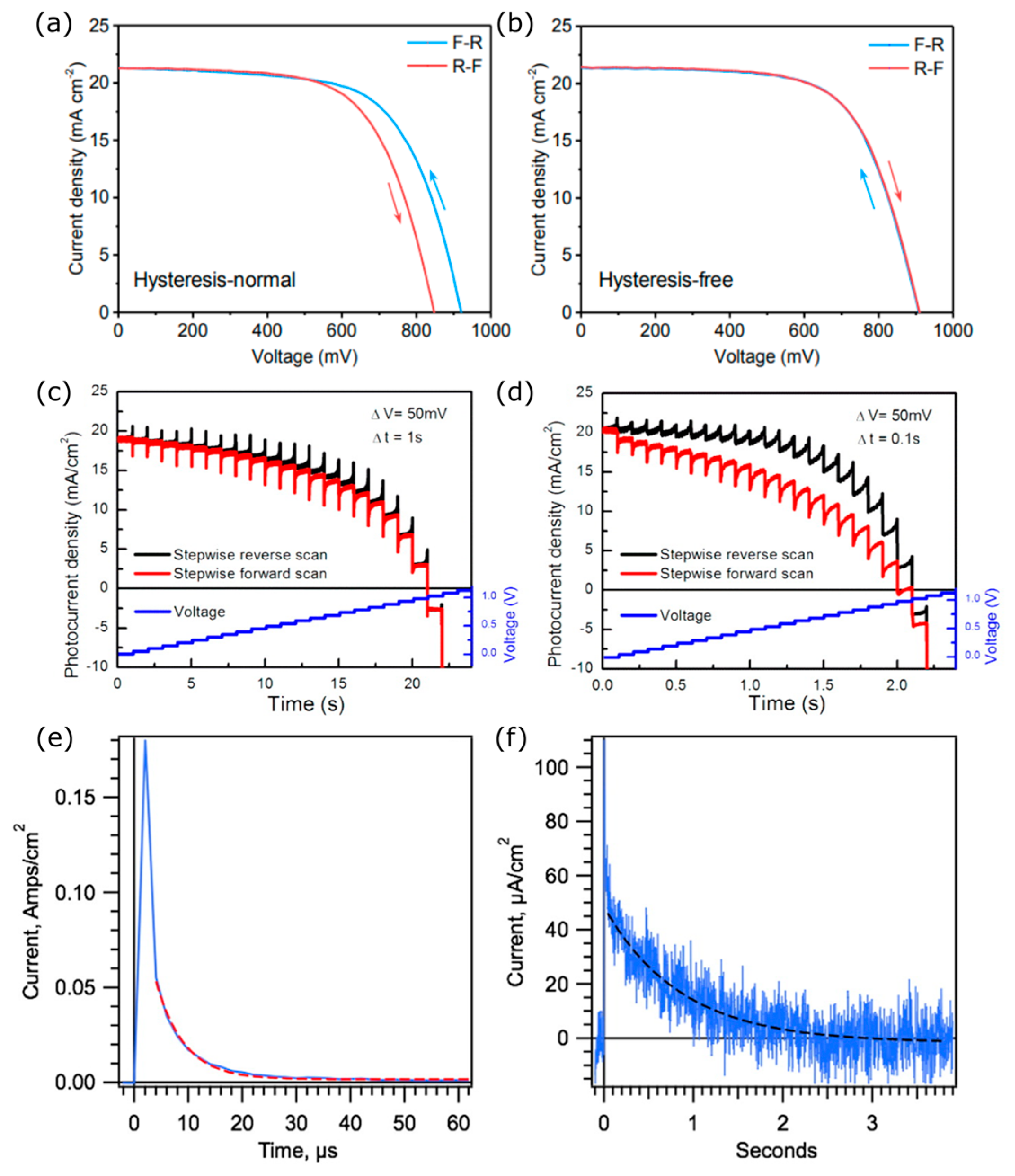
2.3. Hysteresis in PSCs
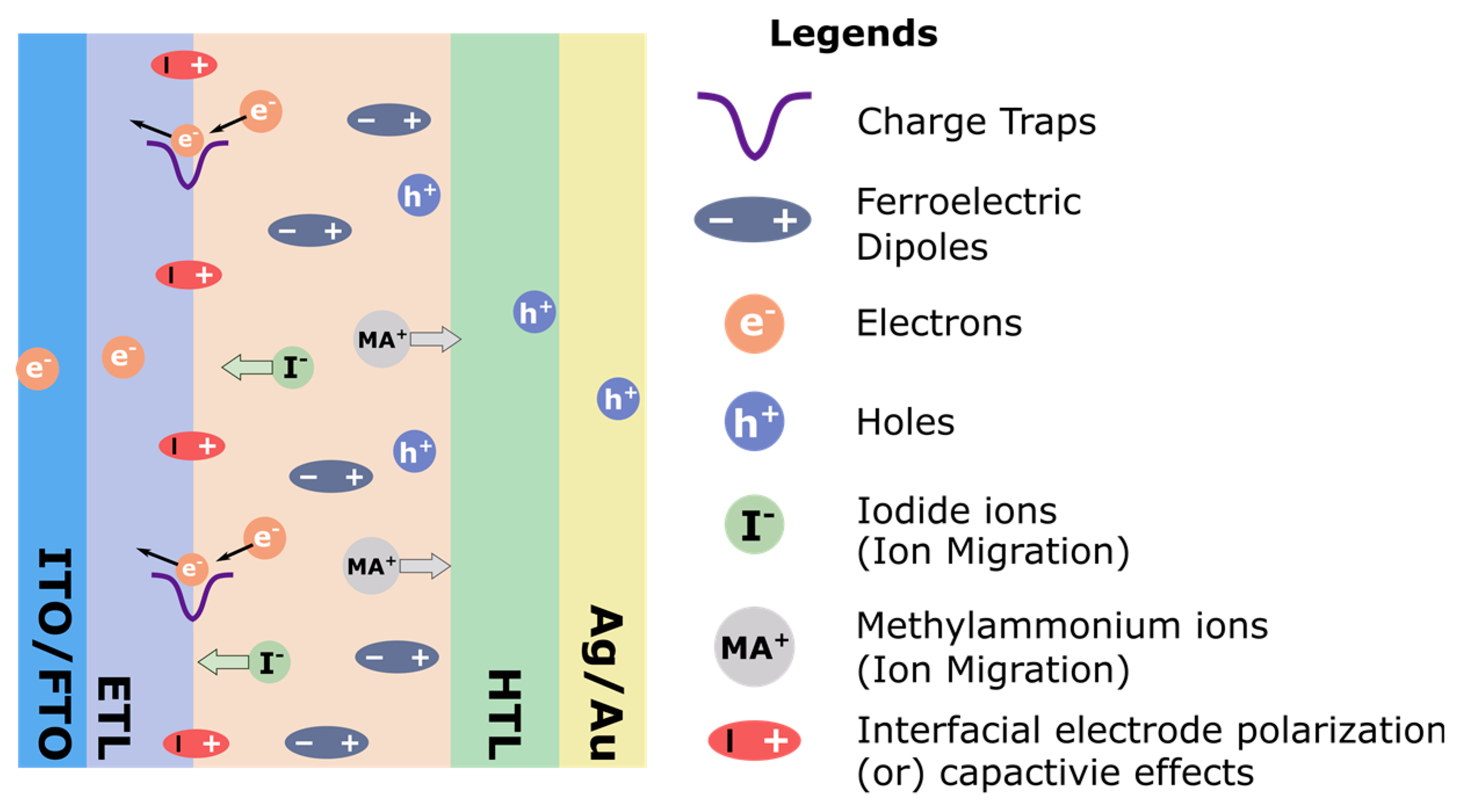
- Charge traps: Charges can become trapped at defects on surfaces or at grain boundaries and induce recombination, reducing the photocurrent.
- Electrons and holes: Similar to charge trapping, electrons and holes can accumulate in transport layers due to defects or imbalances in the carrier mobilities of the electron and hole transport layers.
- Ion migration: Iodide ions and methylammonium ions can migrate to interfaces under applied bias and alter the internal field reducing the efficiency of carrier separation.
- Interfacial electrode polarization: A capacitive polarization may arise due to the accumulation of charges or ions at interfaces and cause an energy barrier to carrier extraction.

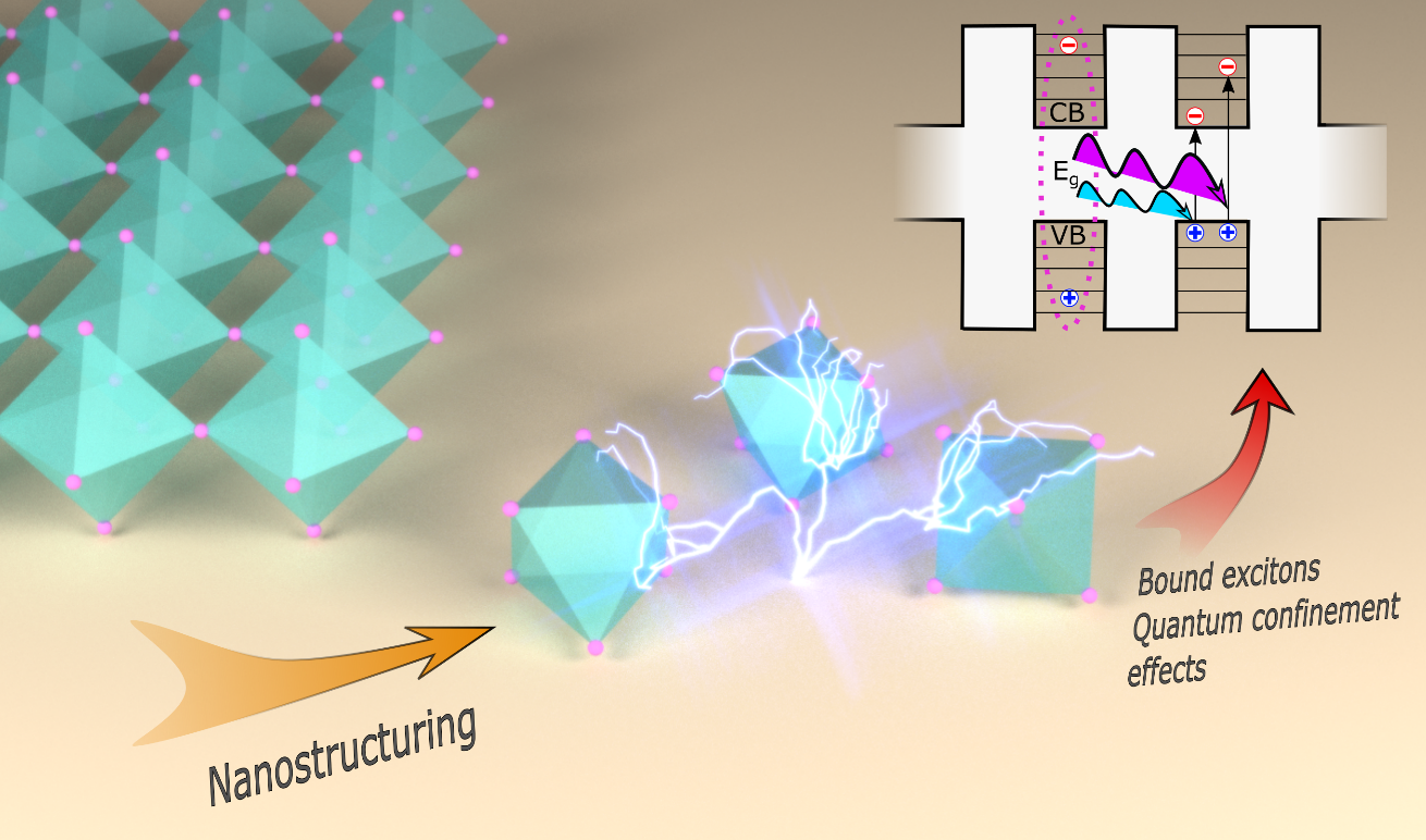
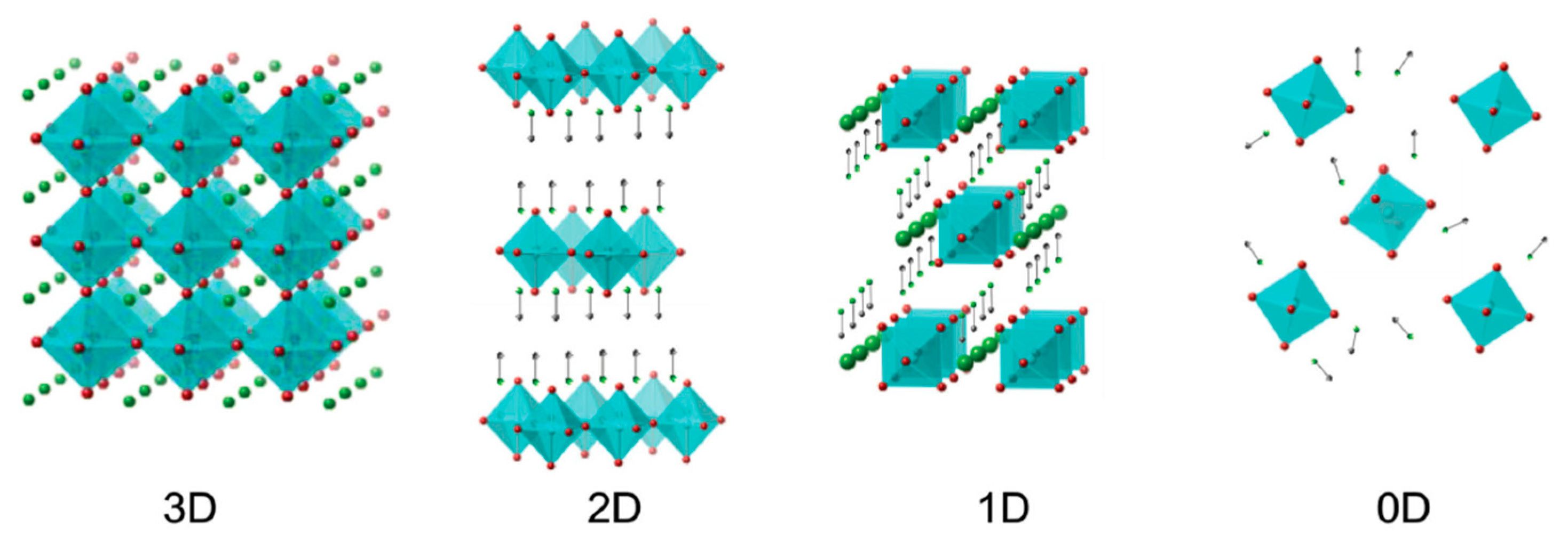
3. Nanostructured Perovskite Absorbers
3.1. Introduction
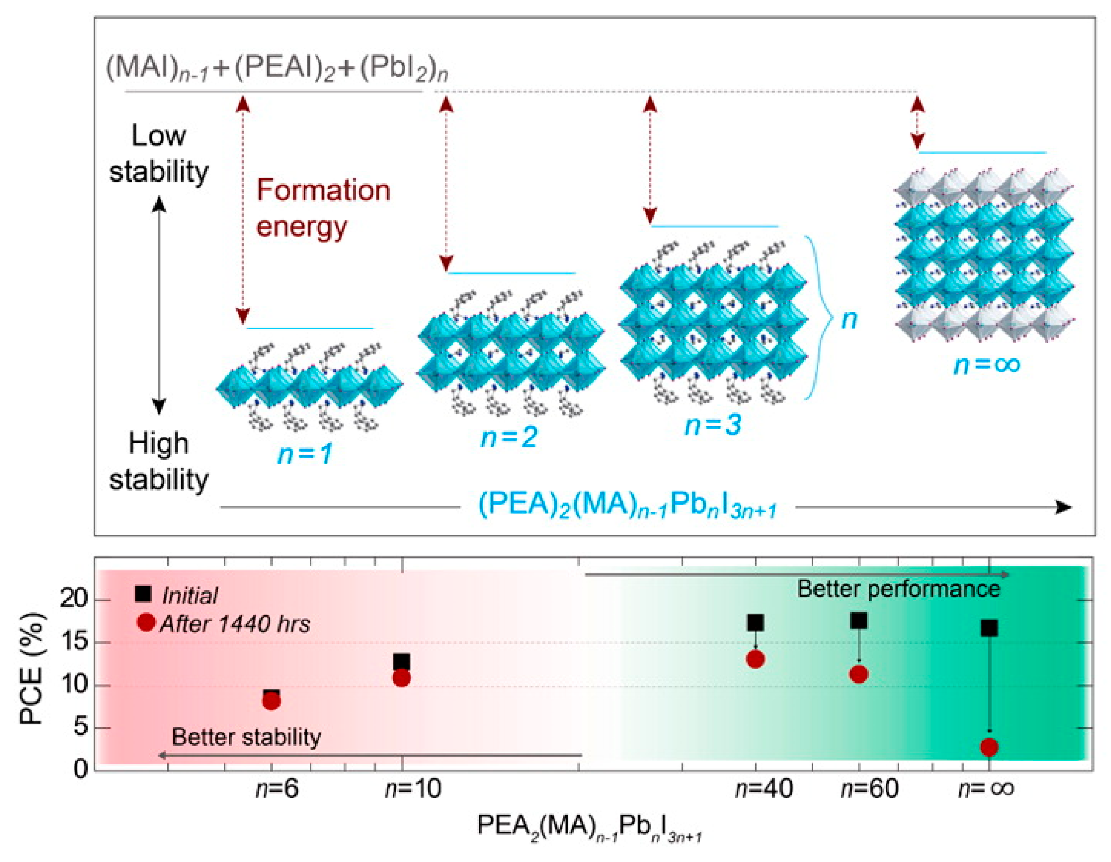
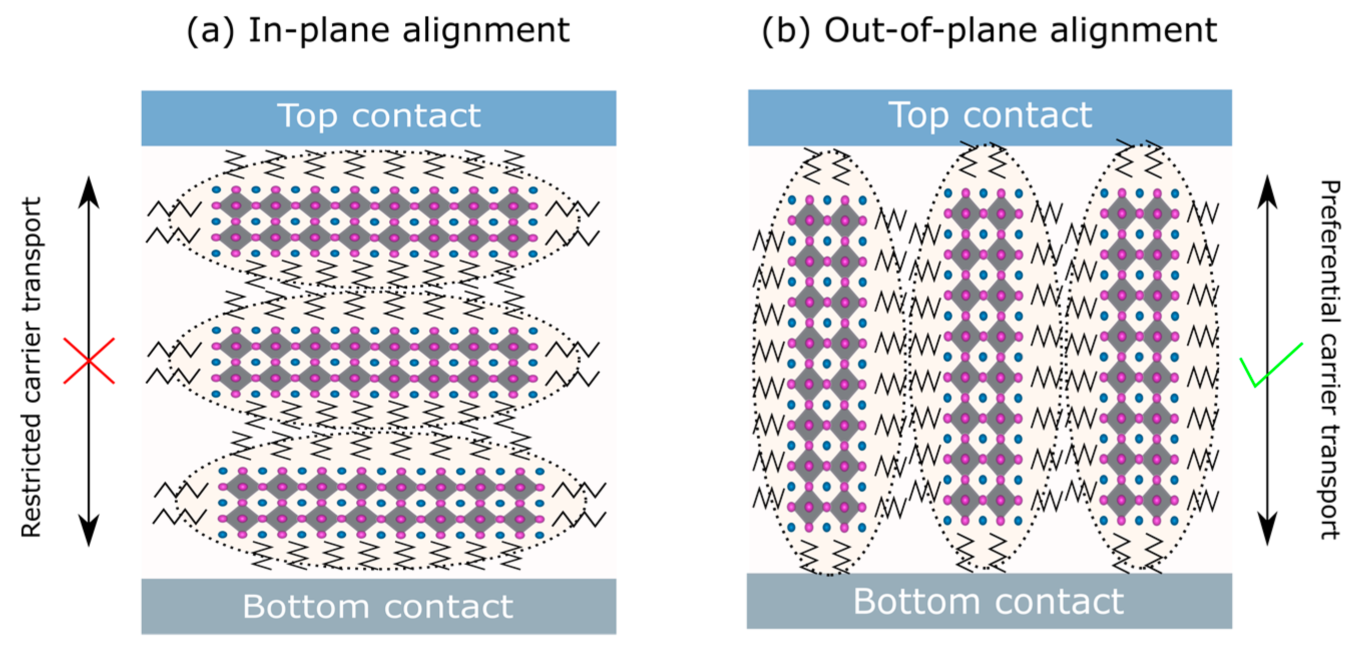
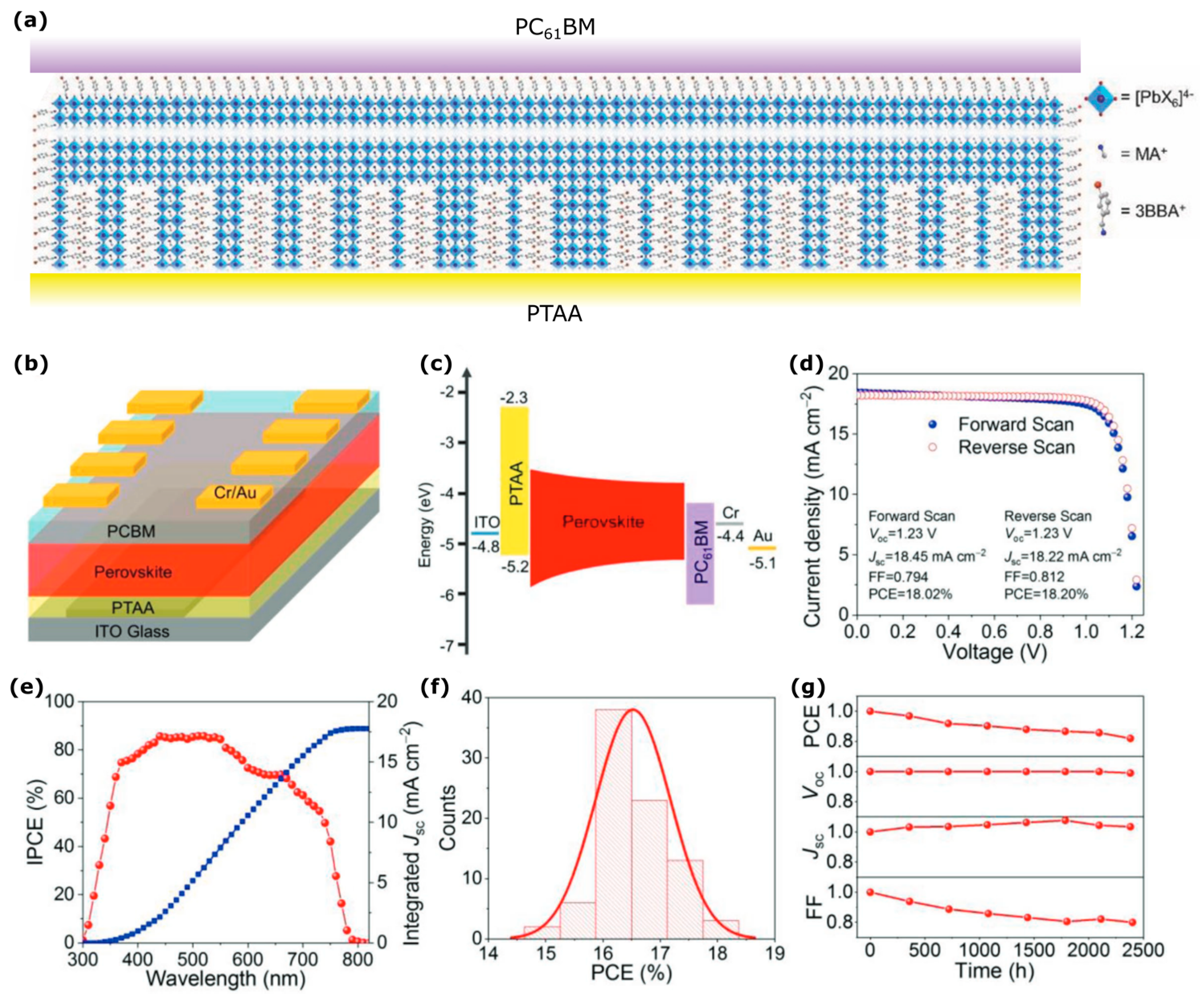
3.2. One- and Two-Dimensional Perovskites
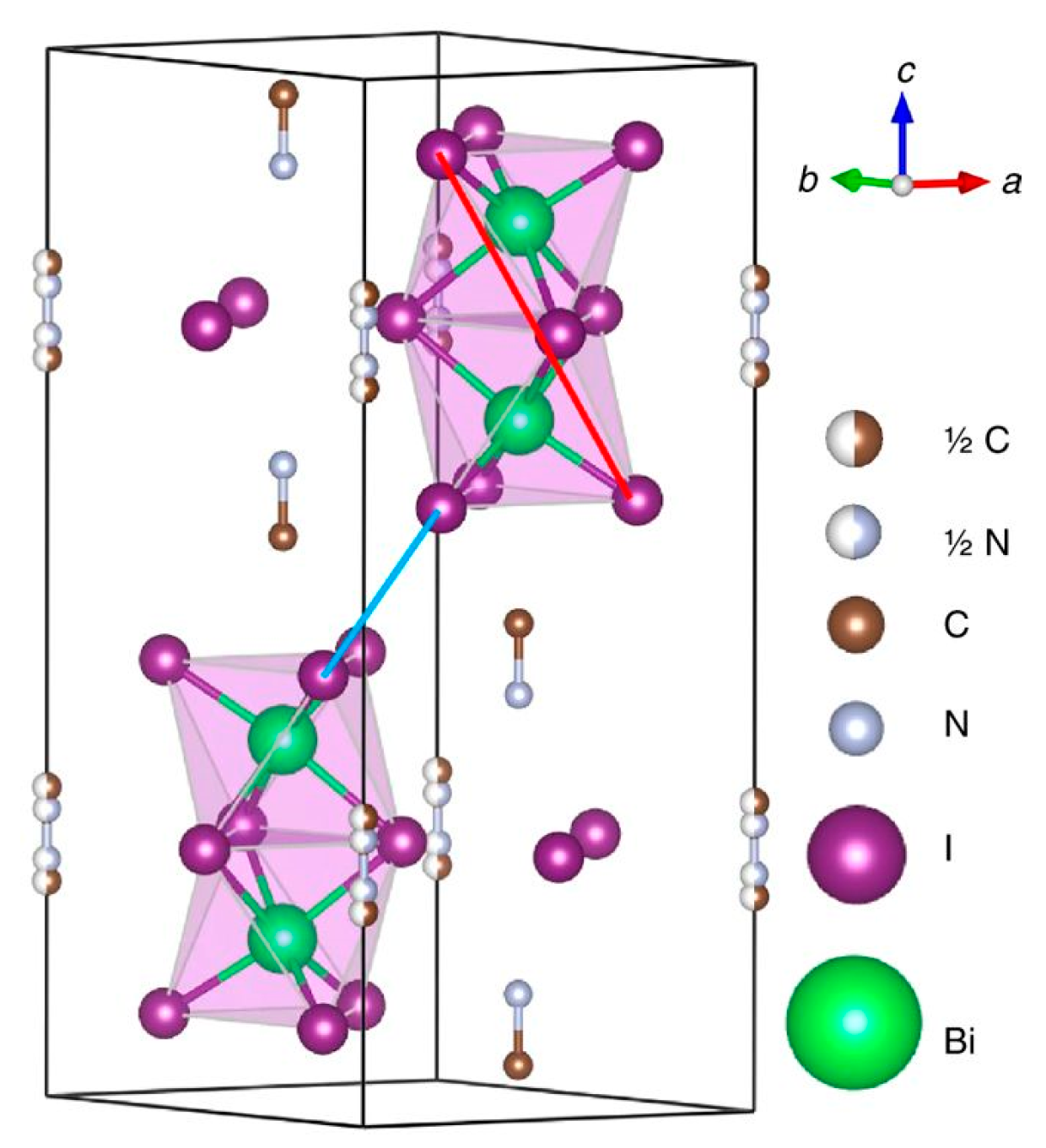
3.3. Zero-Dimensional Perovskites
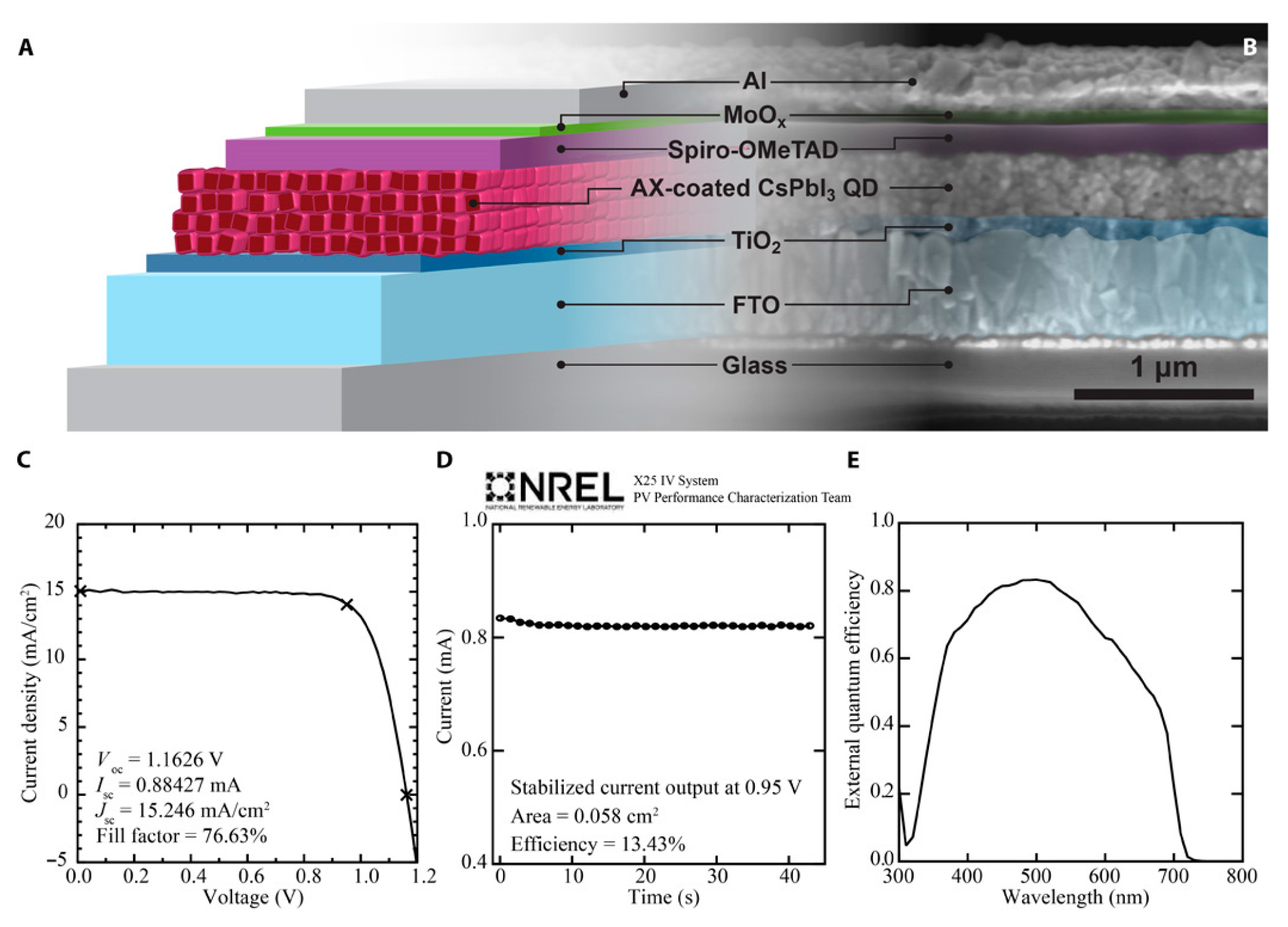
3.4. Perovskite Quantum Dot Solar Cells
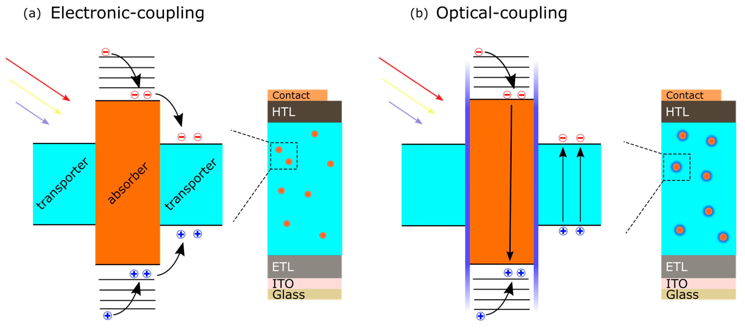
3.5. Perovskite-Nanocrystal Hybrid Devices
3.6. Perovskite Oxide Nanoparticles
4. Conclusions and Outlook
Funding
Conflicts of Interest
References
- National Renewable Energy Laboratory Best Research-Cell Efficiency Chart. Available online: https://www.nrel.gov/pv/assets/pdfs/best-research-cell-efficiencies.20190923.pdf (accessed on 25 September 2019).
- Green, M.A.; Hishikawa, Y.; Dunlop, E.D.; Levi, D.H.; Hohl-Ebinger, J.; Ho-Baillie, A.W.Y. Solar cell efficiency tables (version 52). Prog. Photovolt. Res. Appl. 2018, 26, 427–436. [Google Scholar] [CrossRef]
- Leijtens, T.; Bush, K.A.; Prasanna, R.; McGehee, M.D. Opportunities and challenges for tandem solar cells using metal halide perovskite semiconductors. Nat. Energy 2018, 1–11. [Google Scholar] [CrossRef]
- Jung, H.S.; Park, N.-G. Perovskite Solar Cells: From Materials to Devices. Small 2015, 11, 10–25. [Google Scholar] [CrossRef] [PubMed]
- Xing, G.; Mathews, N.; Sun, S.; Lim, S.S.; Lam, Y.M.; Gratzel, M.; Mhaisalkar, S.; Sum, T.C. Long-Range Balanced Electron- and Hole-Transport Lengths in Organic-Inorganic CH3NH3PbI3. Science 2013, 342, 344–347. [Google Scholar] [CrossRef] [PubMed]
- Stranks, S.D.; Eperon, G.E.; Grancini, G.; Menelaou, C.; Alcocer, M.J.P.; Leijtens, T.; Herz, L.M.; Petrozza, A.; Snaith, H.J. Electron-hole diffusion lengths exceeding 1 micrometer in an organometal trihalide perovskite absorber. Science 2013, 342, 341–344. [Google Scholar] [CrossRef] [PubMed]
- Lin, Q.; Armin, A.; Nagiri, R.C.R.; Burn, P.L.; Meredith, P. Electro-optics of perovskite solar cells. Nat. Photonics 2014, 9, 106–112. [Google Scholar] [CrossRef]
- Xing, G.; Mathews, N.; Lim, S.S.; Yantara, N.; Liu, X.; Sabba, D.; Grätzel, M.; Mhaisalkar, S.; Sum, T.C. Low-temperature solution-processed wavelength-tunable perovskites for lasing. Nat. Mater. 2014, 13, 476–480. [Google Scholar] [CrossRef]
- Xing, J.; Zhao, Y.; Askerka, M.; Quan, L.N.; Gong, X.; Zhao, W.; Zhao, J.; Tan, H.; Long, G.; Gao, L.; et al. Color-stable highly luminescent sky-blue perovskite light-emitting diodes. Nat. Commun. 2018, 9. [Google Scholar] [CrossRef]
- Li, Z.; Moon, J.; Gharajeh, A.; Haroldson, R.; Hawkins, R.; Hu, W.; Zakhidov, A.; Gu, Q. Room-temperature continuous-wave operation of organometal halide perovskite lasers. ACS Nano 2018, 12, 10968–10976. [Google Scholar] [CrossRef]
- Wang, K.; Wang, S.; Xiao, S.; Song, Q. Recent Advances in Perovskite Micro- and Nanolasers. Adv. Opt. Mater. 2018, 6, 1800278. [Google Scholar] [CrossRef]
- Feng, J.; Gong, C.; Gao, H.; Wen, W.; Gong, Y.; Jiang, X.; Zhang, B.; Wu, Y.; Wu, Y.; Fu, H.; et al. Single-crystalline layered metal-halide perovskite nanowires for ultrasensitive photodetectors. Nat. Electron. 2018, 1, 404–410. [Google Scholar] [CrossRef]
- Saliba, M.; Matsui, T.; Seo, J.-Y.; Domanski, K.; Correa-Baena, J.-P.; Mohammad, K.N.; Zakeeruddin, S.M.; Tress, W.; Abate, A.; Hagfeldt, A.; et al. Cesium-containing Triple Cation Perovskite Solar Cells: Improved Stability, Reproducibility and High Efficiency. Energy Environ. Sci. 2016, 9, 1989–1997. [Google Scholar] [CrossRef] [PubMed]
- Jeon, N.J.; Noh, J.H.; Yang, W.S.; Kim, Y.C.; Ryu, S.; Seo, J.; Seok, S. Il Compositional engineering of perovskite materials for high-performance solar cells. Nature 2015, 517, 476–480. [Google Scholar] [CrossRef] [PubMed]
- Li, X.; Bi, D.; Yi, C.; Decoppet, J.-D.; Luo, J.; Zakeeruddin, S.M.; Hagfeldt, A.; Gratzel, M. A vacuum flash-assisted solution process for high-efficiency large-area perovskite solar cells. Science 2016, 353, 58–62. [Google Scholar] [CrossRef] [PubMed]
- Eperon, G.E.; Stranks, S.D.; Menelaou, C.; Johnston, M.B.; Herz, L.M.; Snaith, H.J. Formamidinium lead trihalide: A broadly tunable perovskite for efficient planar heterojunction solar cells. Energy Environ. Sci. 2014, 7, 982–988. [Google Scholar] [CrossRef]
- Seok, S.I.; Grätzel, M.; Park, N.G. Methodologies toward Highly Efficient Perovskite Solar Cells. Small 2018, 14. [Google Scholar] [CrossRef]
- Huang, F.; Li, M.; Siffalovic, P.; Cao, G.; Tian, J. From scalable solution fabrication of perovskite films towards commercialization of solar cells. Energy Environ. Sci. 2019, 12, 518–549. [Google Scholar] [CrossRef]
- Cheacharoen, R.; Rolston, N.; Harwood, D.; Bush, K.A.; Dauskardt, R.H.; McGehee, M.D. Design and understanding of encapsulated perovskite solar cells to withstand temperature cycling. Energy Environ. Sci. 2018, 11, 144–150. [Google Scholar] [CrossRef]
- Fan, X.; Zhang, M.; Wang, X.; Yang, F.; Meng, X.; Chen, C.W.M.; Tang, C.Y.; Chen, C.W.M.; Cao, J.; Wang, Z.G.; et al. Recent progress in organic–inorganic hybrid solar cells. 2013, 1, 8694–8709. J. Mater. Chem. A 2013, 1, 8694–8709. [Google Scholar] [CrossRef]
- Sanehira, E.M.; Marshall, A.R.; Christians, J.A.; Harvey, S.P.; Ciesielski, P.N.; Wheeler, L.M.; Schulz, P.; Lin, L.Y.; Beard, M.C.; Luther, J.M. Enhanced mobility CsPbI3 quantum dot arrays for record-efficiency, high-voltage photovoltaic cells. Sci. Adv. 2017, 3, eaao4204. [Google Scholar] [CrossRef]
- Quan, L.N.; Yuan, M.; Comin, R.; Voznyy, O.; Beauregard, E.M.; Hoogland, S.; Buin, A.; Kirmani, A.R.; Zhao, K.; Amassian, A.; et al. Ligand-Stabilized Reduced-Dimensionality Perovskites. J. Am. Chem. Soc. 2016, 138, 2649–2655. [Google Scholar] [CrossRef] [PubMed]
- Tsai, H.; Nie, W.; Blancon, J.-C.; Stoumpos, C.C.; Asadpour, R.; Harutyunyan, B.; Neukirch, A.J.; Verduzco, R.; Crochet, J.J.; Tretiak, S.; et al. High-efficiency two-dimensional Ruddlesden–Popper perovskite solar cells. Nature 2016, 536, 312–316. [Google Scholar] [CrossRef] [PubMed]
- Yang, R.; Li, R.; Cao, Y.; Wei, Y.; Miao, Y.; Tan, W.L.; Jiao, X.; Chen, H.; Zhang, L.; Chen, Q.; et al. Oriented Quasi-2D Perovskites for High Performance Optoelectronic Devices. Adv. Mater. 2018, 30, 1804771. [Google Scholar] [CrossRef] [PubMed]
- Kim, M.R.; Ma, D. Quantum-Dot-Based Solar Cells: Recent Advances, Strategies, and Challenges. J. Phys. Chem. Lett. 2015, 6, 85–99. [Google Scholar] [CrossRef]
- Lee, M.M.; Teuscher, J.; Miyasaka, T.; Murakami, T.N.; Snaith, H.J. Efficient hybrid solar cells based on meso-superstructured organometal halide perovskites. Science 2012, 338, 643–647. [Google Scholar] [CrossRef]
- Kim, H.-S.; Lee, C.-R.; Im, J.-H.; Lee, K.-B.; Moehl, T.; Marchioro, A.; Moon, S.-J.; Humphry-Baker, R.; Yum, J.-H.; Moser, J.E.; et al. Lead Iodide Perovskite Sensitized All-Solid-State Submicron Thin Film Mesoscopic Solar Cell with Efficiency Exceeding 9%. Sci. Rep. 2012, 2, 591. [Google Scholar] [CrossRef]
- Xiong, L.; Guo, Y.; Wen, J.; Liu, H.; Yang, G.; Qin, P.; Fang, G. Review on the Application of SnO2 in Perovskite Solar Cells. Adv. Funct. Mater. 2018, 28. [Google Scholar] [CrossRef]
- Yang, W.S.; Park, B.-W.; Jung, E.H.; Jeon, N.J.; Kim, Y.C.; Lee, D.U.; Shin, S.S.; Seo, J.; Kim, E.K.; Noh, J.H.; et al. Iodide management in formamidinium-lead-halide-based perovskite layers for efficient solar cells. Science 2017, 356, 1376–1379. [Google Scholar] [CrossRef]
- Hoye, R.L.Z.; Brandt, R.E.; Osherov, A.; Stevanovic, V.; Stranks, S.D.; Wilson, M.W.B.; Kim, H.; Akey, A.J.; Perkins, J.D.; Kurchin, R.C.; et al. Methylammonium Bismuth Iodide as a Lead-Free, Stable Hybrid Organic-Inorganic Solar Absorber. Chem. A Eur. J. 2016, 22, 2605–2610. [Google Scholar] [CrossRef]
- Zhang, L.; Ju, M.-G.; Liang, W. The effect of moisture on the structures and properties of lead halide perovskites: A first-principles theoretical investigation. Phys. Chem. Chem. Phys. 2016, 18, 23174–23183. [Google Scholar] [CrossRef]
- Rocks, C.; Svrcek, V.; Maguire, P.; Mariotti, D. Understanding Surface Chemistry During MAPbI3 Spray Deposition and its Effect on Photovoltaic Performance. J. Mater. Chem. C 2017, 5, 902–916. [Google Scholar] [CrossRef]
- Ahn, N.; Kwak, K.; Jang, M.S.; Yoon, H.; Lee, B.Y.; Lee, J.-K.; Pikhitsa, P.V.; Byun, J.; Choi, M. Trapped charge-driven degradation of perovskite solar cells. Nat. Commun. 2016, 7, 13422. [Google Scholar] [CrossRef] [PubMed]
- Hoke, E.T.; Slotcavage, D.J.; Dohner, E.R.; Bowring, A.R.; Karunadasa, H.I.; McGehee, M.D. Reversible photo-induced trap formation in mixed-halide hybrid perovskites for photovoltaics. Chem. Sci. 2015, 6, 613–617. [Google Scholar] [CrossRef] [PubMed]
- Wu, B.; Fu, K.; Yantara, N.; Xing, G.; Sun, S.; Sum, T.C.; Mathews, N. Charge Accumulation and Hysteresis in Perovskite-Based Solar Cells: An Electro-Optical Analysis. Adv. Energy Mater. 2015, 5, 1500829. [Google Scholar] [CrossRef]
- deQuilettes, D.W.; Zhang, W.; Burlakov, V.M.; Graham, D.J.; Leijtens, T.; Osherov, A.; Bulović, V.; Snaith, H.J.; Ginger, D.S.; Stranks, S.D. Photo-induced halide redistribution in organic–inorganic perovskite films. Nat. Commun. 2016, 7, 11683. [Google Scholar] [CrossRef]
- Choi, J.J.; Yang, X.; Norman, Z.M.; Billinge, S.J.L.; Owen, J.S. Structure of Methylammonium Lead Iodide Within Mesoporous Titanium Dioxide: Active Material in High-Performance Perovskite Solar Cells. Nano Lett. 2014, 14, 127–133. [Google Scholar] [CrossRef]
- Jeon, N.J.; Noh, J.H.; Kim, Y.C.; Yang, W.S.; Ryu, S.; Seok, S. Il Solvent engineering for high-performance inorganic–organic hybrid perovskite solar cells. Nat. Mater. 2014, 13, 897–903. [Google Scholar] [CrossRef]
- Misra, R.K.; Aharon, S.; Li, B.; Mogilyansky, D.; Visoly-Fisher, I.; Etgar, L.; Katz, E.A. Temperature- and Component-Dependent Degradation of Perovskite Photovoltaic Materials under Concentrated Sunlight. J. Phys. Chem. Lett. 2015, 6, 326–330. [Google Scholar] [CrossRef]
- Bush, K.A.; Palmstrom, A.F.; Yu, Z.J.; Boccard, M.; Cheacharoen, R.; Mailoa, J.P.; McMeekin, D.P.; Hoye, R.L.Z.; Bailie, C.D.; Leijtens, T.; et al. 23.6%-efficient monolithic perovskite/silicon tandem solar cells with improved stability. Nat. Energy 2017, 2, 17009. [Google Scholar] [CrossRef]
- Wang, S.; Jiang, Y.; Juarez-Perez, E.J.; Ono, L.K.; Qi, Y. Accelerated degradation of methylammonium lead iodide perovskites induced by exposure to iodine vapour. Nat. Energy 2016, 2, 395–398. [Google Scholar] [CrossRef]
- Juarez-Perez, E.J.; Ono, L.K.; Maeda, M.; Jiang, Y.; Hawash, Z.; Qi, Y. Photodecomposition and thermal decomposition in methylammonium halide lead perovskites and inferred design principles to increase photovoltaic device stability. J. Mater. Chem. A 2018, 6, 9604–9612. [Google Scholar] [CrossRef]
- Babayigit, A.; Ethirajan, A.; Muller, M.; Conings, B. Toxicity of organometal halide perovskite solar cells. Nat. Mater. 2016, 15, 247–251. [Google Scholar] [CrossRef] [PubMed]
- Park, N.-G.; Grätzel, M.; Miyasaka, T.; Zhu, K.; Emery, K. Towards stable and commercially available perovskite solar cells. Nat. Energy 2016, 1, 16152. [Google Scholar] [CrossRef]
- Clever, H.L.; Johnston, F.J. The solubility of some sparingly soluble lead salts: An evaluation of the solubility in water and aqueous electrolyte solution. J. Phys. Chem. Ref. Data 1982, 9, 751–784. [Google Scholar] [CrossRef]
- Filip, M.R.; Giustino, F. Computational Screening of Homovalent Lead Substitution in Organic-Inorganic Halide Perovskites. J. Phys. Chem. C 2016, 120, 166–173. [Google Scholar] [CrossRef]
- Yin, W.J.; Shi, T.; Yan, Y. Unique properties of halide perovskites as possible origins of the superior solar cell performance. Adv. Mater. 2014, 26, 4653–4658. [Google Scholar] [CrossRef] [PubMed]
- Lee, S.J.; Shin, S.S.; Kim, Y.C.; Kim, D.; Ahn, T.K.; Noh, J.H.; Seo, J.; Seok, S. Il Fabrication of Efficient Formamidinium Tin Iodide Perovskite Solar Cells through SnF2–Pyrazine Complex. J. Am. Chem. Soc. 2016, 138, 3974–3977. [Google Scholar] [CrossRef]
- Leijtens, T.; Prasanna, R.; Gold-Parker, A.; Toney, M.F.; McGehee, M.D. Mechanism of Tin Oxidation and Stabilization by Lead Substitution in Tin Halide Perovskites. ACS Energy Lett. 2017, 2, 2159–2165. [Google Scholar] [CrossRef]
- Muscarella, L.A.; Petrova, D.; Jorge Cervasio, R.; Farawar, A.; Lugier, O.; McLure, C.; Slaman, M.J.; Wang, J.; Ehrler, B.; Von Hauff, E.; et al. Air-Stable and Oriented Mixed Lead Halide Perovskite (FA/MA) by the One-Step Deposition Method Using Zinc Iodide and an Alkylammonium Additive. ACS Appl. Mater. Interfaces 2019, 11, 17555–17562. [Google Scholar] [CrossRef]
- Chen, R.; Hou, D.; Lu, C.; Zhang, J.; Liu, P.; Tian, H.; Zeng, Z.; Xiong, Q.; Hu, Z.; Zhu, Y.; et al. Zinc ion as effective film morphology controller in perovskite solar cells. Sustain. Energy Fuels 2018, 2, 1093–1100. [Google Scholar] [CrossRef]
- Kooijman; Muscarella; Williams Perovskite Thin Film Materials Stabilized and Enhanced by Zinc(II) Doping. Appl. Sci. 2019, 9, 1678. [CrossRef]
- Shai, X.; Wang, J.; Sun, P.; Huang, W.; Liao, P.; Cheng, F.; Zhu, B.; Chang, S.Y.; Yao, E.P.; Shen, Y.; et al. Achieving ordered and stable binary metal perovskite via strain engineering. Nano Energy 2018, 48, 117–127. [Google Scholar] [CrossRef]
- Eames, C.; Frost, J.M.; Barnes, P.R.F.; O’Regan, B.C.; Walsh, A.; Islam, M.S. Ionic transport in hybrid lead iodide perovskite solar cells. Nat. Commun. 2015, 6, 7497. [Google Scholar] [CrossRef] [PubMed]
- Meloni, S.; Moehl, T.; Tress, W.; Franckevičius, M.; Saliba, M.; Lee, Y.H.; Gao, P.; Nazeeruddin, M.K.; Zakeeruddin, S.M.; Rothlisberger, U.; et al. Ionic polarization-induced current–voltage hysteresis in CH3NH3PbX3 perovskite solar cells. Nat. Commun. 2016, 7, 10334. [Google Scholar] [CrossRef]
- Tress, W.; Marinova, N.; Moehl, T.; Zakeeruddin, S.M.; Nazeeruddin, M.K.; Grätzel, M. Understanding the rate-dependent J–V hysteresis, slow time component, and aging in CH3NH3PbI3 perovskite solar cells: The role of a compensated electric field. Energy Environ. Sci. 2015, 8, 995–1004. [Google Scholar] [CrossRef]
- Cao, X.; Li, Y.; Li, C.; Fang, F.; Yao, Y.; Cui, X.; Wei, J. Modulating Hysteresis of Perovskite Solar Cells by a Poling Voltage. J. Phys. Chem. C 2016, 120, 22784–22792. [Google Scholar] [CrossRef]
- Yuan, Y.; Huang, J. Ion Migration in Organometal Trihalide Perovskite and Its Impact on Photovoltaic Efficiency and Stability. Acc. Chem. Res. 2016, 49, 286–293. [Google Scholar] [CrossRef]
- Levine, I.; Nayak, P.K.; Wang, J.T.-W.; Sakai, N.; Van Reenen, S.; Brenner, T.M.; Mukhopadhyay, S.; Snaith, H.J.; Hodes, G.; Cahen, D. Temperature-dependent Hysteresis in MAPbI3 Solar Cells. J. Phys. Chem. C 2016. [Google Scholar] [CrossRef]
- Mei, A.; Li, X.; Liu, L.; Ku, Z.; Liu, T.; Rong, Y.; Xu, M.; Hu, M.; Chen, J.; Yang, Y.; et al. A hole-conductor-free, fully printable mesoscopic perovskite solar cell with high stability. Science 2014, 345, 295–298. [Google Scholar] [CrossRef]
- Ko, Y.; Kim, Y.; Lee, C.; Kim, Y.; Jun, Y. Investigation of Hole-Transporting Poly(triarylamine) on Aggregation and Charge Transport for Hysteresisless Scalable Planar Perovskite Solar Cells. ACS Appl. Mater. Interfaces 2018, 10, 11633–11641. [Google Scholar] [CrossRef]
- Wei, J.; Zhao, Y.; Li, H.; Li, G.; Pan, J.; Xu, D.; Zhao, Q.; Yu, D. Hysteresis Analysis Based on the Ferroelectric Effect in Hybrid Perovskite Solar Cells. J. Phys. Chem. Lett. 2014, 5, 3937–3945. [Google Scholar] [CrossRef] [PubMed]
- Unger, E.L.; Hoke, E.T.; Bailie, C.D.; Nguyen, W.H.; Bowring, A.R.; Heumüller, T.; Christoforo, M.G.; McGehee, M.D.; Pullerits, T.; Stepanov, A.; et al. Hysteresis and transient behavior in current–voltage measurements of hybrid-perovskite absorber solar cells. Energy Environ. Sci. 2014, 7, 3690–3698. [Google Scholar] [CrossRef]
- Kim, H.S.; Park, N.G. Parameters affecting I-V hysteresis of CH3NH3PbI3 perovskite solar cells: Effects of perovskite crystal size and mesoporous TiO2 layer. J. Phys. Chem. Lett. 2014, 5, 2927–2934. [Google Scholar] [CrossRef] [PubMed]
- Sanchez, R.S.; Gonzalez-Pedro, V.; Lee, J.-W.; Park, N.-G.; Kang, Y.S.; Mora-Sero, I.; Bisquert, J. Slow Dynamic Processes in Lead Halide Perovskite Solar Cells. Characteristic Times and Hysteresis. J. Phys. Chem. Lett. 2014, 5, 2357–2363. [Google Scholar] [CrossRef]
- Rong, Y.; Hu, Y.; Ravishankar, S.; Liu, H.; Hou, X.; Sheng, Y.; Mei, A.; Wang, Q.; Li, D.; Xu, M.; et al. Tunable hysteresis effect for perovskite solar cells. Energy Environ. Sci. 2017, 10, 2383–2391. [Google Scholar] [CrossRef]
- Chen, B.; Yang, M.; Zheng, X.; Wu, C.; Li, W.; Yan, Y.; Bisquert, J.; Garcia-Belmonte, G.; Zhu, K.; Priya, S. Impact of Capacitive Effect and Ion Migration on the Hysteretic Behavior of Perovskite Solar Cells. J. Phys. Chem. Lett. 2015, 6, 4693–4700. [Google Scholar] [CrossRef]
- O’Regan, B.C.; Barnes, P.R.F.; Li, X.; Law, C.; Palomares, E.; Marin-Beloqui, J.M. Optoelectronic studies of methylammonium lead iodide perovskite solar cells with mesoporous TiO2: Separation of electronic and chemical charge storage, understanding two recombination lifetimes, and the evolution of band offsets during J–V hysteresis. J. Am. Chem. Soc. 2015, 137, 5087–5099. [Google Scholar] [CrossRef]
- Richardson, G.; O’Kane, S.E.J.; Niemann, R.G.; Peltola, T.A.; Foster, J.M.; Cameron, P.J.; Walker, A.B.; Pace, G.; Manna, L.; Caironi, M.; et al. Can slow-moving ions explain hysteresis in the current–voltage curves of perovskite solar cells? Energy Environ. Sci. 2016, 9, 1476–1485. [Google Scholar] [CrossRef]
- Shao, Y.; Xiao, Z.; Bi, C.; Yuan, Y.; Huang, J. Origin and elimination of photocurrent hysteresis by fullerene passivation in CH3NH3PbI3 planar heterojunction solar cells. Nat. Commun. 2014, 5, 5784. [Google Scholar] [CrossRef]
- Zheng, F.; Xin, Y.; Huang, W.; Zhang, J.; Wang, X.; Shen, M.; Dong, W.; Fang, L.; Bai, Y.; Shen, X.; et al. Above 1% Efficiency of a Ferroelectric Solar Cell Based on the Pb({Zr,Ti)O3} Film. J. Mater. Chem. A 2013, 2, 1363–1368. [Google Scholar] [CrossRef]
- Frost, J.M.; Butler, K.T.; Brivio, F.; Hendon, C.H.; van Schilfgaarde, M.; Walsh, A. Atomistic Origins of High-Performance in Hybrid Halide Perovskite Solar Cells. Nano Lett. 2014, 14, 2584–2590. [Google Scholar] [CrossRef] [PubMed]
- Chen, B.; Zheng, X.; Yang, M.; Zhou, Y.; Kundu, S.; Shi, J.; Zhu, K.; Priya, S. Interface band structure engineering by ferroelectric polarization in perovskite solar cells. Nano Energy 2015, 13, 582–591. [Google Scholar] [CrossRef]
- Kutes, Y.; Ye, L.; Zhou, Y.; Pang, S.; Huey, B.D.; Padture, N.P. Direct observation of ferroelectric domains in solution-processed CH3NH3PbI3 perovskite thin films. J. Phys. Chem. Lett. 2014, 5, 3335–3339. [Google Scholar] [CrossRef] [PubMed]
- Kim, H.; Kim, S.K.; Kim, B.J.; Shin, K.; Gupta, M.K.; Jung, H.S.; Kim, S.; Park, N. Ferroelectric Polarization in CH3NH3PbI3 Perovskite. J. Phys. Chem. Lett. 2015, 6, 1729–1735. [Google Scholar] [CrossRef] [PubMed]
- Elumalai, N.K.; Uddin, A. Hysteresis in organic-inorganic hybrid perovskite solar cells. Sol. Energy Mater. Sol. Cells 2016, 157, 476–509. [Google Scholar] [CrossRef]
- Zhang, X.; Wu, G.; Gu, Z.; Guo, B.; Liu, W.; Yang, S.; Ye, T.; Chen, C.; Tu, W.; Chen, H. Active-layer evolution and efficiency improvement of (CH3NH3)3Bi2I9-based solar cell on TiO2-deposited ITO substrate. Nano Res. 2016, 9, 2921–2930. [Google Scholar] [CrossRef]
- Giustino, F.; Snaith, H.J. Towards Lead-free Perovskite Solar Cells. ACS Energy Lett. 2016, 1, 1233–1240. [Google Scholar] [CrossRef]
- González-Carrero, S.; Galian, R.E.; Pérez-Prieto, J. Organometal Halide Perovskites: Bulk Low-Dimension Materials and Nanoparticles. Part. Part. Syst. Charact. 2015, 32, 709–720. [Google Scholar] [CrossRef]
- Müller, M.F.; Freunek, M.; Reindl, L.M. Maximum efficiencies of indoor photovoltaic devices. IEEE J. Photovoltaics 2013, 3, 59–64. [Google Scholar]
- de Weerd, C.; Gomez, L.; Capretti, A.; Lebrun, D.M.; Matsubara, E.; Lin, J.; Ashida, M.; Spoor, F.C.M.; Siebbeles, L.D.A.; Houtepen, A.J.; et al. Efficient carrier multiplication in CsPbI3 perovskite nanocrystals. Nat. Commun. 2018, 9. [Google Scholar] [CrossRef]
- Ni, C.; Hedley, G.; Payne, J.; Svrcek, V.; McDonald, C.; Jagadamma, L.K.; Edwards, P.; Martin, R.; Jain, G.; Carolan, D.; et al. Charge carrier localised in zero-dimensional (CH3NH3)3Bi2I9 clusters. Nat. Commun. 2017, 8. [Google Scholar] [CrossRef]
- Nozik, A.J. Nanoscience and nanostructures for photovoltaics and solar fuels. Nano Lett. 2010, 10, 2735–2741. [Google Scholar] [CrossRef] [PubMed]
- Shockley, W.; Queisser, H.J. Detailed Balance Limit of Efficiency of p-n Junction Solar Cells. J. Appl. Phys. 1961, 32, 510. [Google Scholar] [CrossRef]
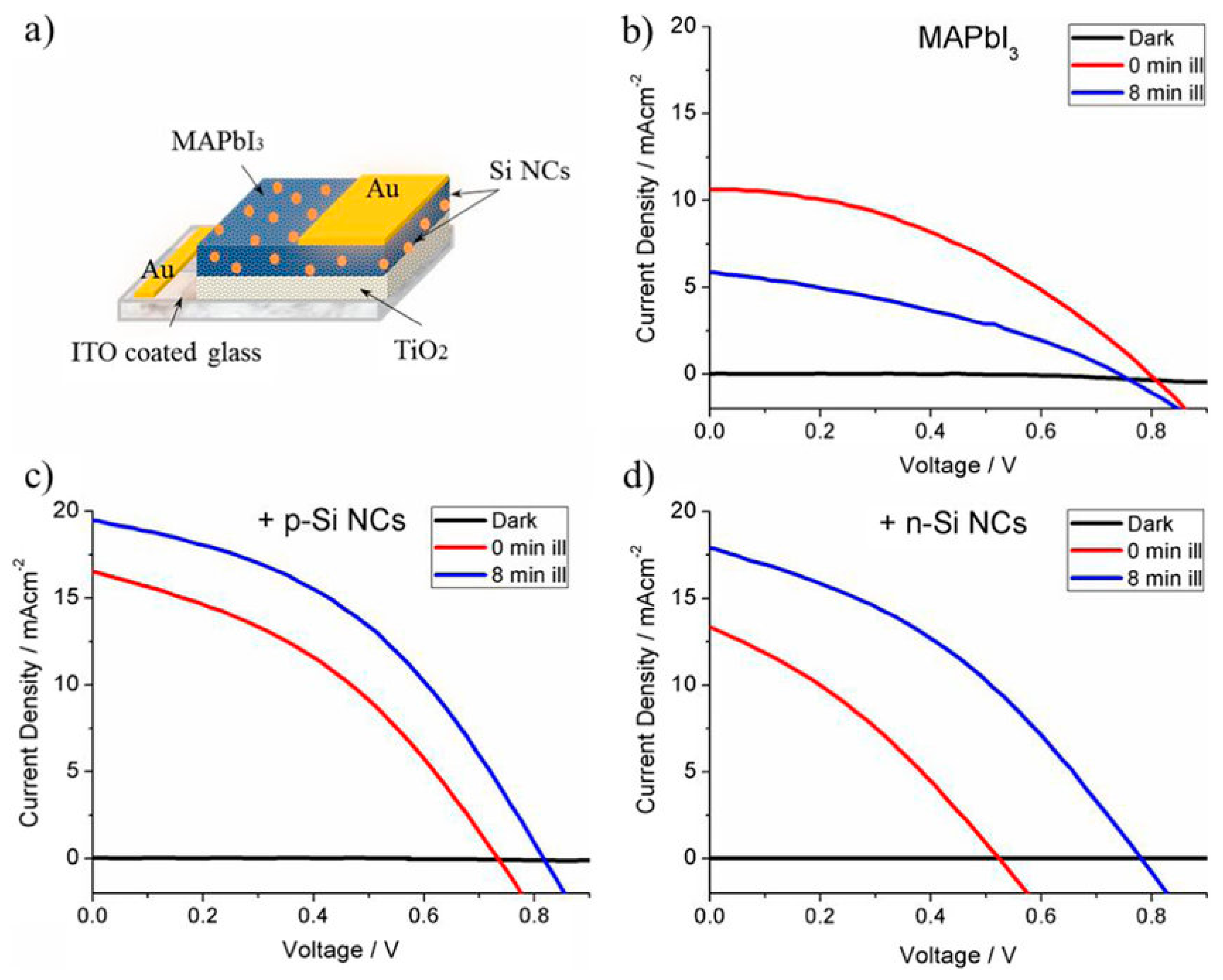
- Rocks, C.; Svrcek, V.; Velusamy, T.; Macias-Montero, M.; Maguire, P.; Mariotti, D. Type-I alignment in MAPbI3 based solar devices with doped-silicon nanocrystals. Nano Energy 2018, 50, 245–255. [Google Scholar] [CrossRef]
- McDonald, C.; Ni, C.; Švrček, V.; Lozac’H, M.; Connor, P.A.; Maguire, P.; Irvine, J.T.S.; Mariotti, D. Zero-dimensional methylammonium iodo bismuthate solar cells and synergistic interactions with silicon nanocrystals. Nanoscale 2017, 9. [Google Scholar] [CrossRef] [PubMed]
- Kawai, T.; Shimanuki, S. Optical Studies of (CH3NH3)3Bi2I9 Single Crystals. Phys. Status Solidi 1993, 177, 43–45. [Google Scholar] [CrossRef]
- Pazoki, M.; Johansson, M.B.; Zhu, H.; Broqvist, P.; Edvinsson, T.; Boschloo, G.; Johansson, E.M.J. Bismuth Iodide Perovskite Materials for Solar Cell Applications: Electronic Structure, Optical Transitions, and Directional Charge Transport. J. Phys. Chem. C 2016, 120, 29039–29046. [Google Scholar] [CrossRef]
- Cao, D.H.; Stoumpos, C.C.; Farha, O.K.; Hupp, J.T.; Kanatzidis, M.G. 2D Homologous Perovskites as Light-Absorbing Materials for Solar Cell Applications. J. Am. Chem. Soc. 2015, 137, 7843–7850. [Google Scholar] [CrossRef]
- Koh, T.M.; Shanmugam, V.; Schlipf, J.; Oesinghaus, L.; Müller-Buschbaum, P.; Ramakrishnan, N.; Swamy, V.; Mathews, N.; Boix, P.P.; Mhaisalkar, S.G. Nanostructuring Mixed-Dimensional Perovskites: A Route Toward Tunable, Efficient Photovoltaics. Adv. Mater. 2016, 28, 3653–3661. [Google Scholar] [CrossRef]
- Yao, K.; Wang, X.; Xu, Y.X.; Li, F.; Zhou, L. Multilayered Perovskite Materials Based on Polymeric-Ammonium Cations for Stable Large-Area Solar Cell. Chem. Mater. 2016, 28, 3131–3138. [Google Scholar] [CrossRef]
- Lai, H.; Kan, B.; Liu, T.; Zheng, N.; Xie, Z.; Zhou, T.; Wan, X.; Zhang, X.; Liu, Y.; Chen, Y. Two-Dimensional Ruddlesden–Popper Perovskite with Nanorod-like Morphology for Solar Cells with Efficiency Exceeding 15%. J. Am. Chem. Soc. 2018, 140, 11639–11646. [Google Scholar] [CrossRef] [PubMed]
- Cohen, B.E.; Wierzbowska, M.; Etgar, L. High efficiency quasi 2D lead bromide perovskite solar cells using various barrier molecules. Sustain. Energy Fuels 2017, 1, 1935–1943. [Google Scholar] [CrossRef]
- Ma, C.; Shen, D.; Ng, T.W.; Lo, M.F.; Lee, C.S. 2D Perovskites with Short Interlayer Distance for High-Performance Solar Cell Application. Adv. Mater. 2018, 30, 1800710. [Google Scholar] [CrossRef] [PubMed]
- Smith, I.C.; Hoke, E.T.; Solis-Ibarra, D.; McGehee, M.D.; Karunadasa, H.I. A Layered Hybrid Perovskite Solar-Cell Absorber with Enhanced Moisture Stability. Angew. Chem. Int. Ed. 2014, 53, 11232–11235. [Google Scholar] [CrossRef]
- Blancon, J.C.; Tsai, H.; Nie, W.; Stoumpos, C.C.; Pedesseau, L.; Katan, C.; Kepenekian, M.; Soe, C.M.M.; Appavoo, K.; Sfeir, M.Y.; et al. Extremely efficient internal exciton dissociation through edge states in layered 2D perovskites. Science 2017, 355, 1288–1292. [Google Scholar] [CrossRef]
- Zhang, X.; Ren, X.; Liu, B.; Munir, R.; Zhu, X.; Yang, D.; Li, J.; Liu, Y.; Smilgies, D.M.; Li, R.; et al. Stable high efficiency two-dimensional perovskite solar cells via cesium doping. Energy Environ. Sci. 2017, 10, 2095–2102. [Google Scholar] [CrossRef]
- Liu, G.; Zheng, H.; Xu, X.; Zhu, L.; Alsaedi, A.; Hayat, T.; Pan, X.; Dai, S. Efficient solar cells with enhanced humidity and heat stability based on benzylammonium–caesium–formamidinium mixed-dimensional perovskites. J. Mater. Chem. A 2018, 6, 18067–18074. [Google Scholar] [CrossRef]
- Liu, Y.; Akin, S.; Pan, L.; Uchida, R.; Arora, N.; Milić, J.V.; Hinderhofer, A.; Schreiber, F.; Uhl, A.R.; Zakeeruddin, S.M.; et al. Ultrahydrophobic 3D/2D fluoroarene bilayer-based water-resistant perovskite solar cells with efficiencies exceeding 22%. Sci. Adv. 2019, 5, eaaw2543. [Google Scholar] [CrossRef]
- Alharbi, E.A.; Alyamani, A.Y.; Kubicki, D.J.; Uhl, A.R.; Walder, B.J.; Alanazi, A.Q.; Luo, J.; Burgos-Caminal, A.; Albadri, A.; Albrithen, H.; et al. Atomic-level passivation mechanism of ammonium salts enabling highly efficient perovskite solar cells. Nat. Commun. 2019. [Google Scholar] [CrossRef]
- Takeoka, Y.; Asai, K.; Rikukawa, M.; Sanui, K. Hydrothermal Synthesis and Structure of Zero-dimensional Organic–inorganic Perovskites. Chem. Lett. 2005, 34, 602–603. [Google Scholar] [CrossRef]
- Akkerman, Q.A.; Abdelhady, A.L.; Manna, L. Zero-Dimensional Cesium Lead Halides: History, Properties, and Challenges. J. Phys. Chem. Lett. 2018, 9, 2326–2337. [Google Scholar] [CrossRef] [PubMed]
- Park, B.W.; Philippe, B.; Zhang, X.; Rensmo, H.; Boschloo, G.; Johansson, E.M.J. Bismuth Based Hybrid Perovskites A3Bi2I9 (A: Methylammonium or Cesium) for Solar Cell Application. Adv. Mater. 2015, 27, 6806–6813. [Google Scholar] [CrossRef] [PubMed]
- Qiu, X.; Jiang, Y.; Zhang, H.; Qiu, Z.; Yuan, S.; Wang, P.; Cao, B. Lead-free mesoscopic Cs2SnI6 perovskite solar cells using different nanostructured ZnO nanorods as electron transport layers. Phys. Status Solidi - Rapid Res. Lett. 2016, 10, 587–591. [Google Scholar] [CrossRef]
- Zhang, Z.; Li, X.; Xia, X.; Wang, Z.; Huang, Z.; Lei, B.; Gao, Y. High-Quality (CH3NH3)3Bi2I9Film-Based Solar Cells: Pushing Efficiency up to 1.64%. J. Phys. Chem. Lett. 2017, 8, 4300–4307. [Google Scholar] [CrossRef] [PubMed]
- Zhu, H.; Pan, M.; Johansson, M.B.; Johansson, E.M.J. High Photon-to-Current Conversion in Solar Cells Based on Light-Absorbing Silver Bismuth Iodide. ChemSusChem 2017, 10, 2592–2596. [Google Scholar] [CrossRef]
- Vigneshwaran, M.; Ohta, T.; Iikubo, S.; Kapil, G.; Ripolles, T.S.; Ogomi, Y.; Ma, T.; Pandey, S.S.; Shen, Q.; Toyoda, T.; et al. Facile synthesis and characterization of sulfur doped low bandgap bismuth based perovskites by soluble precursor route. Chem. Mater. 2016, 28, 6436–6440. [Google Scholar] [CrossRef]
- Kim, Y.; Yang, Z.; Jain, A.; Voznyy, O.; Kim, G.-H.; Liu, M.; Quan, L.N.; García de Arquer, F.P.; Comin, R.; Fan, J.Z.; et al. Pure Cubic-Phase Hybrid Iodobismuthates AgBi2I7 for Thin-Film Photovoltaics. Angew. Chem. 2016, 128, 9738–9742. [Google Scholar] [CrossRef]
- Karuppuswamy, P.; Boopathi, K.M.; Mohapatra, A.; Chen, H.C.; Wong, K.T.; Wang, P.C.; Chu, C.W. Role of a hydrophobic scaffold in controlling the crystallization of methylammonium antimony iodide for efficient lead-free perovskite solar cells. Nano Energy 2018, 45, 330–336. [Google Scholar] [CrossRef]
- Chatterjee, S.; Pal, A.J. Tin(IV) Substitution in (CH3NH3)3Sb2I9: Toward Low-Band-Gap Defect-Ordered Hybrid Perovskite Solar Cells. ACS Appl. Mater. Interfaces 2018, 10, acsami.8b12018. [Google Scholar] [CrossRef]
- Correa-Baena, J.P.; Nienhaus, L.; Kurchin, R.C.; Shin, S.S.; Wieghold, S.; Putri Hartono, N.T.; Layurova, M.; Klein, N.D.; Poindexter, J.R.; Polizzotti, A.; et al. A-Site Cation in Inorganic A3Sb2I9 Perovskite Influences Structural Dimensionality, Exciton Binding Energy, and Solar Cell Performance. Chem. Mater. 2018, 30, 3734–3742. [Google Scholar] [CrossRef]
- Ghosh, B.; Wu, B.; Mulmudi, H.K.; Guet, C.; Weber, K.; Sum, T.C.; Mhaisalkar, S.; Mathews, N. Limitations of Cs3Bi2I9 as Lead-Free Photovoltaic Absorber Materials. ACS Appl. Mater. Interfaces 2018, 10, 35000–35007. [Google Scholar] [CrossRef] [PubMed]
- Ha, S.T.; Su, R.; Xing, J.; Zhang, Q.; Xiong, Q. Metal halide perovskite nanomaterials: Synthesis and applications. Chem. Sci. 2017, 8, 2522–2536. [Google Scholar] [CrossRef] [PubMed]
- Swarnkar, A.; Marshall, A.R.; Sanehira, E.M.; Chernomordik, B.D.; Moore, D.T.; Christians, J.A.; Chakrabarti, T.; Luther, J.M. Quantum dot–induced phase stabilization of α-CsPbI3 perovskite for high-efficiency photovoltaics. Science 2016, 354, 92–95. [Google Scholar] [CrossRef] [PubMed]
- Eperon, G.E.; Paternò, G.M.; Sutton, R.J.; Zampetti, A.; Haghighirad, A.A.; Cacialli, F.; Snaith, H.J. Inorganic caesium lead iodide perovskite solar cells. J. Mater. Chem. A 2015, 3, 19688–19695. [Google Scholar] [CrossRef]
- Ling, X.; Zhou, S.; Yuan, J.; Shi, J.; Qian, Y.; Larson, B.W.; Zhao, Q.; Qin, C.; Li, F.; Shi, G.; et al. 14.1% CsPbI3 Perovskite Quantum Dot Solar Cells via Cesium Cation Passivation. Adv. Energy Mater. 2019, 9, 1900721. [Google Scholar] [CrossRef]
- Zhao, Q.; Hazarika, A.; Chen, X.; Harvey, S.P.; Larson, B.W.; Teeter, G.R.; Liu, J.; Song, T.; Xiao, C.; Shaw, L.; et al. High efficiency perovskite quantum dot solar cells with charge separating heterostructure. Nat. Commun. 2019, 10, 2842. [Google Scholar] [CrossRef]
- Umar, F.; Zhang, J.; Jin, Z.; Muhammad, I.; Yang, X.; Deng, H.; Jahangeer, K.; Hu, Q.; Song, H.; Tang, J. Dimensionality Controlling of Cs3Sb2I9 for Efficient All-Inorganic Planar Thin Film Solar Cells by HCl-Assisted Solution Method. Adv. Opt. Mater. 2019, 7, 1801368. [Google Scholar] [CrossRef]
- Singh, A.; Boopathi, K.M.; Mohapatra, A.; Chen, Y.F.; Li, G.; Chu, C.W. Photovoltaic Performance of Vapor-Assisted Solution-Processed Layer Polymorph of Cs 3 Sb 2 I 9. ACS Appl. Mater. Interfaces 2018, 10, 2566–2573. [Google Scholar] [CrossRef]
- Ma, C.; Shen, D.; Huang, B.; Li, X.; Chen, W.C.; Lo, M.F.; Wang, P.; Hon-Wah Lam, M.; Lu, Y.; Ma, B.; et al. High performance low-dimensional perovskite solar cells based on a one dimensional lead iodide perovskite. J. Mater. Chem. A 2019, 7, 8811–8817. [Google Scholar] [CrossRef]
- Zhang, F.; Kim, D.H.; Lu, H.; Park, J.S.; Larson, B.W.; Hu, J.; Gao, L.; Xiao, C.; Reid, O.G.; Chen, X.; et al. Enhanced Charge Transport in 2D Perovskites via Fluorination of Organic Cation. J. Am. Chem. Soc. 2019, 141, 5972–5979. [Google Scholar] [CrossRef]
- Cohen, B.E.; Li, Y.; Meng, Q.; Etgar, L. Dion-Jacobson Two-Dimensional Perovskite Solar Cells Based on Benzene Dimethanammonium Cation. Nano Lett. 2019, 19, 2588–2597. [Google Scholar] [CrossRef] [PubMed]
- Zheng, H.; Liu, G.; Zhu, L.; Ye, J.; Zhang, X.; Alsaedi, A.; Hayat, T.; Pan, X.; Dai, S. The Effect of Hydrophobicity of Ammonium Salts on Stability of Quasi-2D Perovskite Materials in Moist Condition. Adv. Energy Mater. 2018, 8. [Google Scholar] [CrossRef]
- Liu, J.J.; Erogbogbo, F.; Yong, K.-T.; Ye, L.; Liu, J.J.; Hu, R.; Chen, H.; Hu, Y.; Yang, Y.; Yang, J.; et al. Assessing clinical prospects of silicon quantum dots: Studies in mice and monkeys. ACS Nano 2013, 7, 7303–7310. [Google Scholar] [CrossRef] [PubMed]
- Mariotti, D.; Mitra, S.; Švrček, V.; Svrček, V. Surface-engineered silicon nanocrystals. Nanoscale 2013, 5, 1385. [Google Scholar] [CrossRef]
- Dasog, M.; Bader, K.; Veinot, J.G.C. Influence of Halides on the Optical Properties of Silicon Quantum Dots. Chem. Mater. 2015, 27, 1153–1156. [Google Scholar] [CrossRef]
- Ramos, E.; Monroy, B.M.; Alonso, J.C.; Sansores, L.E.; Salcedo, R.; Mart, A. Theoretical Study of the Electronic Properties of Silicon Nanocrystals Partially Passivated with Cl and F. J. Phys. Chem. C 2012, 36, 3988–3994. [Google Scholar] [CrossRef]
- Ding, Y.; Sugaya, M.; Liu, Q.; Zhou, S.; Nozaki, T. Oxygen passivation of silicon nanocrystals: Influences on trap states, electron mobility, and hybrid solar cell performance. Nano Energy 2014, 10, 322–328. [Google Scholar] [CrossRef]
- Liu, C.-Y.; Holman, Z.C.; Kortshagen, U.R. Hybrid solar cells from P3HT and silicon nanocrystals. Nano Lett. 2009, 9, 449–452. [Google Scholar] [CrossRef]
- Nie, W.; Blancon, J.-C.; Neukirch, A.J.; Appavoo, K.; Tsai, H.; Chhowalla, M.; Alam, M.A.; Sfeir, M.Y.; Katan, C.; Even, J.; et al. Light-activated photocurrent degradation and self-healing in perovskite solar cells. Nat. Commun. 2016, 7, 11574. [Google Scholar] [CrossRef]
- Rühle, S.; Anderson, A.Y.; Barad, H.N.; Kupfer, B.; Bouhadana, Y.; Rosh-Hodesh, E.; Zaban, A. All-oxide photovoltaics. J. Phys. Chem. Lett. 2012, 3, 3755–3764. [Google Scholar] [CrossRef]
- Nechache, R.; Harnagea, C.; Li, S.; Cardenas, L.; Huang, W.; Chakrabartty, J.; Rosei, F. Bandgap tuning of multiferroic oxide solar cells. Nat. Photonics 2014, 9, 61–67. [Google Scholar] [CrossRef]
- Fan, Z.; Sun, K.; Wang, J. Perovskites for photovoltaics: A combined review of organic–inorganic halide perovskites and ferroelectric oxide perovskites. J. Mater. Chem. A 2015, 3, 18809–18828. [Google Scholar] [CrossRef]
- Lv, M.; Xie, Y.; Wang, Y.; Sun, X.; Wu, F.; Chen, H.; Wang, S.; Shen, C.; Chen, Z.; Ni, S.; et al. Bismuth and chromium co-doped strontium titanates and their photocatalytic properties under visible light irradiation. Phys. Chem. Chem. Phys. 2015, 17, 26320–26329. [Google Scholar] [CrossRef] [PubMed]
- Xu, X.; Randorn, C.; Efstathiou, P.; Irvine, J.T.S. A red metallic oxide photocatalyst. Nat. Mater. 2012, 11, 595–598. [Google Scholar] [CrossRef] [PubMed]
- Yashima, M.; Fumi, U.; Nakano, H.; Omoto, K.; Hester, J.R. Crystal Structure, Optical Properties, and Electronic Structure of Calcium Strontium Tungsten Oxynitrides CaxSr1-xWO2N. J. Phys. Chem. C 2013, 117, 18529–18539. [Google Scholar] [CrossRef]
- Shi, J.; Ye, J.; Zhou, Z.; Li, M.; Guo, L. Hydrothermal Synthesis of Na0.5La0.5TiO3-LaCrO3 Solid-Solution Single-Crystal Nanocubes for Visible-Light-Driven Photocatalytic H2 Evolution. Chem. A Eur. J. 2011, 17, 7858–7867. [Google Scholar] [CrossRef]
- Grinberg, I.; West, D.V.; Torres, M.; Gou, G.; Stein, D.M.; Wu, L.; Chen, G.; Gallo, E.M.; Akbashev, A.R.; Davies, P.K.; et al. Perovskite Oxides for Visible-Light-Absorbing Ferroelectric and Photovoltaic Materials. Nature 2013, 503, 509–512. [Google Scholar] [CrossRef]
- Peña, M.A.; Fierro, J.L.G. Chemical Structures and Performance of Perovskite Oxides. Chem. Rev. 2001, 101, 1981–2018. [Google Scholar]
- Sun, C.; Searles, D.J. Electronics, Vacancies, Optical Properties, and Band Engineering of Red Photocatalyst SrNbO3: A Computational Investigation. J. Phys. Chem. C 2014, 118, 11267–11270. [Google Scholar] [CrossRef]
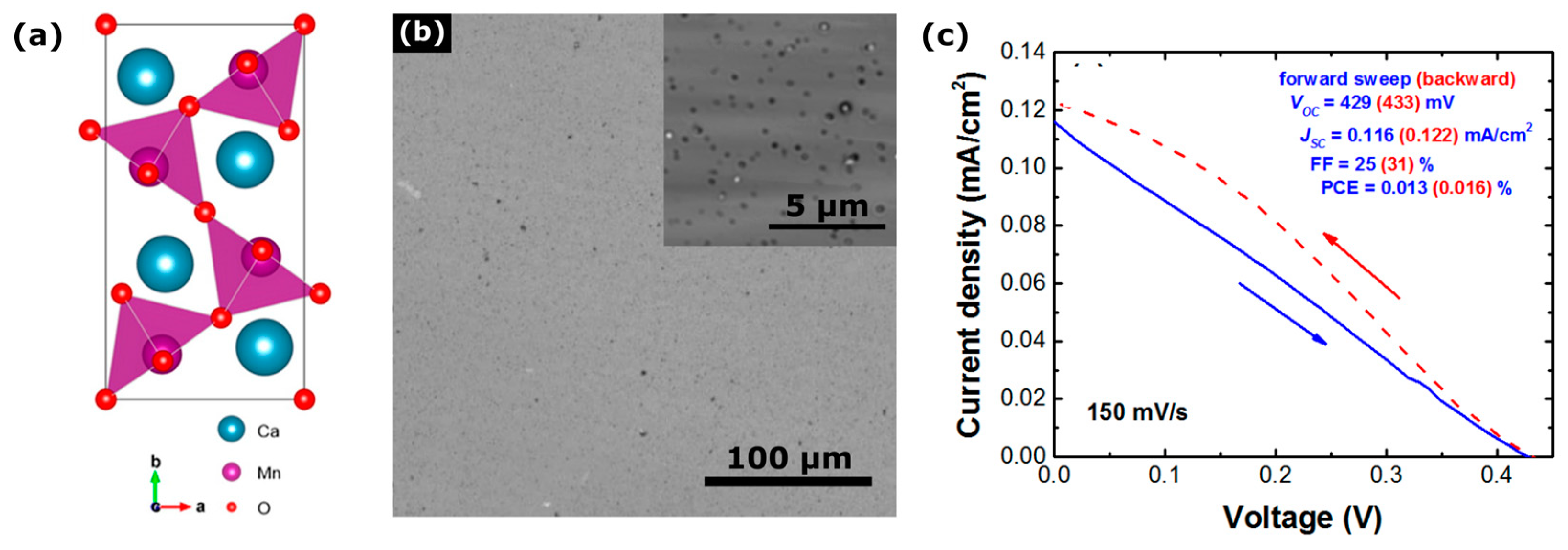
- Kim, J.; Yin, X.; Tsao, K.C.; Fang, S.; Yang, H. Ca2Mn2O5 as Oxygen-Deficient Perovskite Electrocatalyst for Oxygen Evolution Reaction. J. Am. Chem. Soc. 2014, 136, 14646–14649. [Google Scholar] [CrossRef]


| Dimensionality | Material (n Value) 1 | PCE (%) | Stability | Reference (Year) |
|---|---|---|---|---|
| 0D | (CH3NH3)3Sb2I9 | 2.77 | Retained 80% of initial PCE after 3 h under constant illumination, ambient conditions, encapsulated. | [109] (2018) |
| 0D | Cs3Sb2I9 | 1.21 | Retained 95% of initial PCE after 60 days, intermittent measurements, stored at RT, 50% RH, unencapsulated. | [118] (2019) |
| 0D | Cs3Sb2I9 | 1.49 | Retained >80% of initial PCE after 30 days, intermittent measurements, storage conditions unspecified. | [119] (2018) |
| 1D | (ThMA)2(MA)n−1PbnI3n+1 (n = 3) | 15.42 | Retained 90% of initial PCE after 100 h, intermittent, stored in N2 in the dark, unencapsulated. | [92] (2018) |
| 1D, mixed with 3D MAPbI3 | 1,4-benzene diammonium (BDA)-PbI4 (n = 1) | 14.1 | Retained 95% of original PCE after >1000 h, intermittent measurement, stored in dark at RT, 85% RH, encapsulated. | [120] (2019) |
| 1D/3D heterostructure | ethylammonium iodide (EAI)-treated FA0.93Cs0.07PbI3 | 22.3 | Retained 95% of initial PCE after 550 h, continuous measurement under constant illumination in N2 atmosphere at RT, unencapsulated. | [100] (2019) |
| 2D | (FPEA)2MA4Pb5I16 (n = 5) | 13.64 | Retained 65% of initial PCE after 576 h, ambient air at 70 °C unencapsulated. | [121] (2019) |
| 2D | (BzDA)A9Pb10 (I0.93Br0.07)31 (n = 10) | 15.6 | Retained 80% of initial PCE after 84 h, intermittent measurements, kept in dark at RT in ambient air, RH = 20–50% unencapsulated. | [122] (2019) |
| Quasi-2D | 3-bromobenzylammonium iodide (BBAI)- (n = 2) | 18.2 | Retained 82% of initial PCE after 2400 h, intermittent measurements, stored in dark at RT, ~40% RH, unencapsulated. | [24] (2018) |
| Quasi-2D | (BE)2 (FA)8Pb9I28 (n value not reported) | 17.4 | Retained 80% of initial PCE after 50 h, stored in the dark at RT, RH = 80%, unencapsulated. | [123] (2018) |
| QDs | CsPbI3 | 14.1 | Retained 70% of initial PCE after 50 h, intermittent measurements, stored in the dark at RT and 40% RH, unencapsulated. | [116] (2019) |
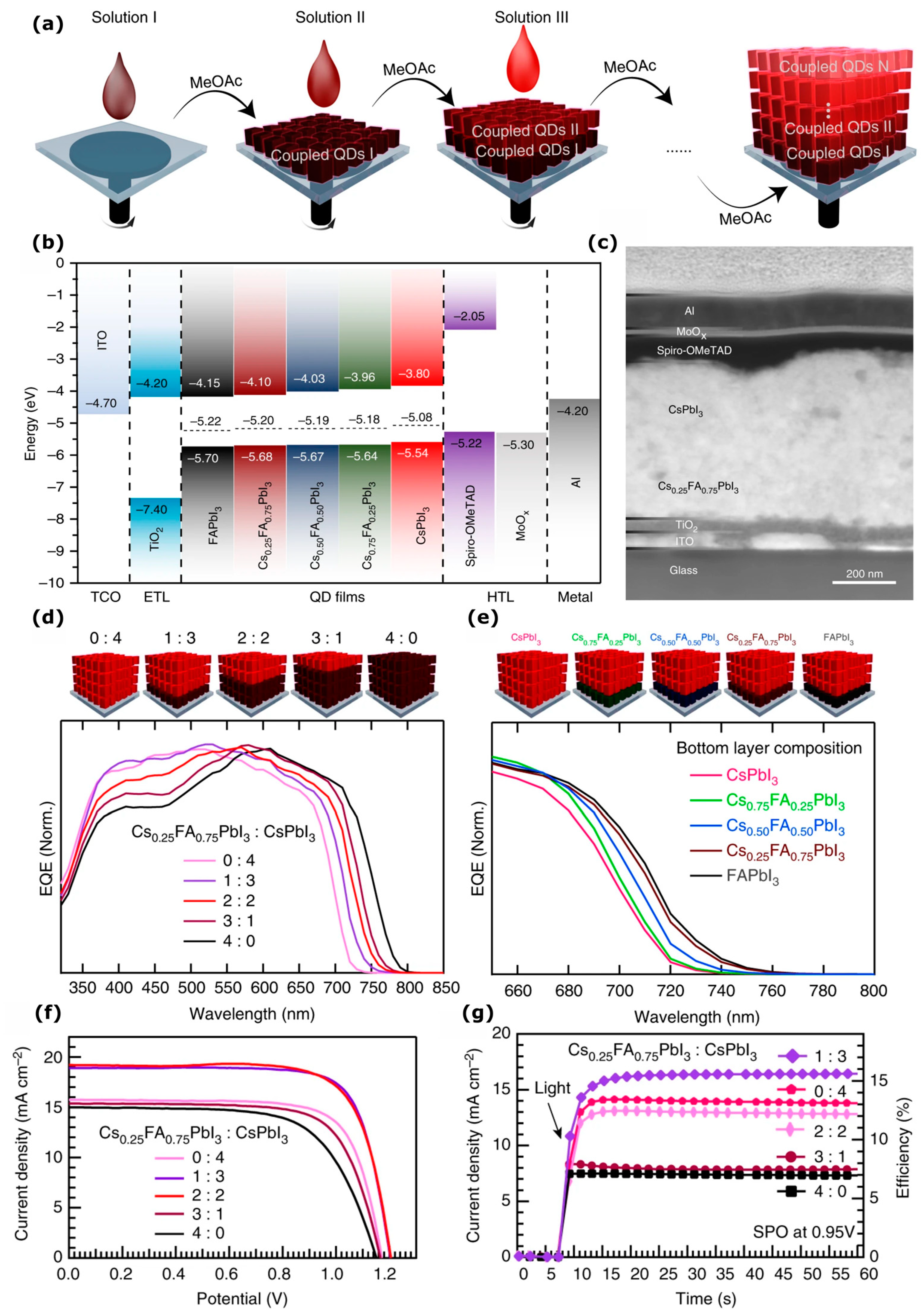
| QDs | CsPbI3:Cs0.25FA0.75PbI3 | 17.4 | Retained 80% of initial PCE after 10 h, intermittent measurements under constant illumination at 40 °C and 25% RH, encapsulated. | [117] (2019) |
© 2019 by the authors. Licensee MDPI, Basel, Switzerland. This article is an open access article distributed under the terms and conditions of the Creative Commons Attribution (CC BY) license (http://creativecommons.org/licenses/by/4.0/).
Share and Cite
McDonald, C.; Ni, C.; Maguire, P.; Connor, P.; Irvine, J.T.S.; Mariotti, D.; Svrcek, V. Nanostructured Perovskite Solar Cells. Nanomaterials 2019, 9, 1481. https://doi.org/10.3390/nano9101481
McDonald C, Ni C, Maguire P, Connor P, Irvine JTS, Mariotti D, Svrcek V. Nanostructured Perovskite Solar Cells. Nanomaterials. 2019; 9(10):1481. https://doi.org/10.3390/nano9101481
Chicago/Turabian StyleMcDonald, Calum, Chengsheng Ni, Paul Maguire, Paul Connor, John T. S. Irvine, Davide Mariotti, and Vladimir Svrcek. 2019. "Nanostructured Perovskite Solar Cells" Nanomaterials 9, no. 10: 1481. https://doi.org/10.3390/nano9101481
APA StyleMcDonald, C., Ni, C., Maguire, P., Connor, P., Irvine, J. T. S., Mariotti, D., & Svrcek, V. (2019). Nanostructured Perovskite Solar Cells. Nanomaterials, 9(10), 1481. https://doi.org/10.3390/nano9101481