Review on Quasi One-Dimensional CdSe Nanomaterials: Synthesis and Application in Photodetectors


Abstract
1. Introduction
2. Synthesis of One-Dimensional (1D) Cadmium Selenide (CdSe) Nanomaterials
2.1. Vapor-Liquid-Solid Method
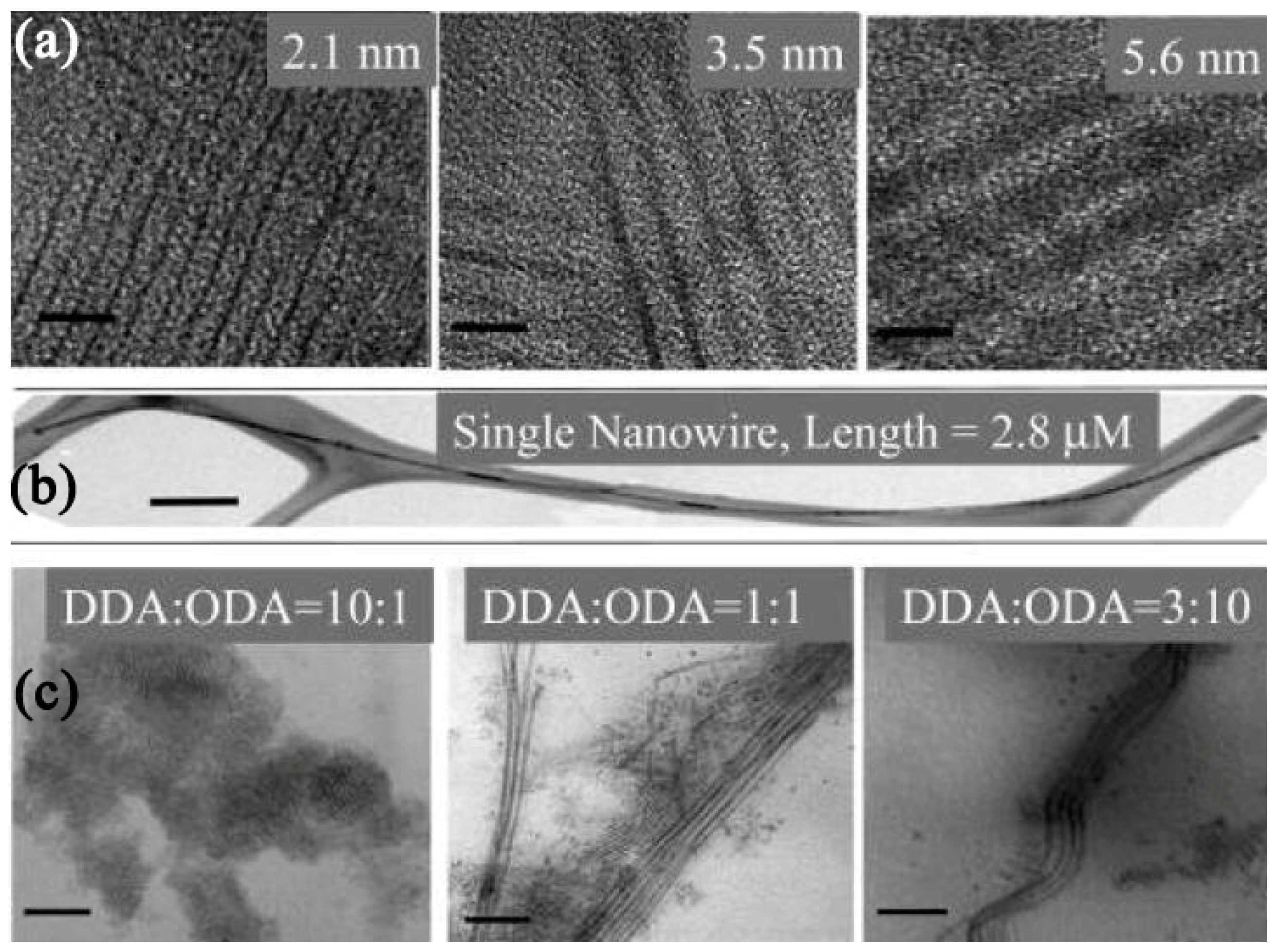
2.2. Solution-Liquid-Solid Method
2.3. Electrochemical Deposition
2.4. Other Methods
3. Application of 1D CdSe Nanomaterials in Photodetectors
3.1. Performance Parameters of Photodetectors
- (1)
- Photocurrent (Iph): defined as the current contribution due to the absorption of signal light.
- (2)
- Dark current (Id): defined as the output current of photodetectors in the absence of illumination.
- (3)
- Responsivity (R): defined as the photocurrent generated per unit power of incident light on the effective area of a photodetector. , in which Iph is the photocurrent, and Pin is the power of incident light. The unit of R is A/W.
- (4)
- External quantum efficiency (η): defined as the ratio of the number of photogenerated electron-hole pairs per second to the number of incident photons per second. , in which h is the Planck constant, ʋ is the frequency of signal light, and q is the elementary charge.
- (5)
- Gain (G): defined as the number of charges collected by the electrodes for each absorbed incident photon. , in which τ is the lifetime of excess carrier, l is the channel length, τtr is the carrier transit time across the channel, V is the applied voltage bias, and μ is the carrier mobility.
- (6)
- Response time: defined as the time for the photocurrent of a photodetector to increase (decay) from 10% (90%) to 90% (10%) after receiving (removing) signal light, which is also named as rising/falling time.
- (7)
- Specific detectivity (D*): used to evaluate the capability of a photodetector in weak light detection. , in which A is the effective area of a photodetector, B is the electrical bandwidth, and NEP is the signal power that produces a signal-to-noise ratio to be equal to 1. The unit of D* is cm·Hz·0.5·W–1 (Jones).
3.2. Photodetectors Based on 1D CdSe Nanomaterials
3.2.1. Photodiodes
3.2.2. Photoconductors
3.2.3. Phototransistors
3.2.4. Some New Mechanisms
4. Summary and Outlook
Author Contributions
Funding
Conflicts of Interest
References
- Tolbert, S.H.; Alivisatos, A.P. The wurtzite to rock salt structural transformation in CdSe nanocrystals under high pressure. J. Chem. Phys. 1995, 102, 4642–4656. [Google Scholar] [CrossRef]
- Kobayashi, A.; Sankey, O.F.; Dow, J.D. Deep energy levels of defects in the wurtzite semiconductors AIN, CdS, CdSe, ZnS, and ZnO. Phys. Rev. B 1983, 28, 946–956. [Google Scholar] [CrossRef]
- Rosen, D.L.; Li, Q.X.; Alfano, R.R. Native defects in undoped semi-insulating CdSe studied by photoluminescence and absorption. Phys. Rev. B 1985, 31, 2396–2403. [Google Scholar] [CrossRef] [PubMed]
- An, Q.; Meng, X.; Xiong, K.; Qiu, Y. A high-performance fully nanostructured individual CdSe nanotube photodetector with enhanced responsivity and photoconductive gain. J. Mate. Chem. C 2017, 5, 7057–7066. [Google Scholar] [CrossRef]
- Jin, W.; Mu, X.; Zhang, K.; Shang, Z.; Dai, L. Influence of interface inhomogeneity on the electrical transport mechanism of CdSe nanowire/Au Schottky junctions. Phys. Chem. Chem. Phys. 2018, 20, 19932–19937. [Google Scholar] [CrossRef] [PubMed]
- Jin, W.; Liu, Y.; Yuan, K.; Zhang, K.; Ye, Y.; Wei, W.; Dai, L. Barrier height inhomogeneity in mixed-dimensional graphene/single CdSe nanobelt Schottky junctions. IEEE Electron. Device Lett. 2019, 40, 119–122. [Google Scholar] [CrossRef]
- Choi, H.; Radich, J.G.; Kamat, P.V. Sequentially layered CdSe/CdS nanowire architecture for improved nanowire solar cell performance. J. Phys. Chem. C 2014, 118, 206–213. [Google Scholar] [CrossRef]
- Ye, Y.; Gan, L.; Dai, L.; Dai, Y.; Guo, X.; Meng, H.; Yu, B.; Shi, Z.; Shang, K.; Qin, G. A simple and scalable graphene patterning method and its application in CdSe nanobelt/graphene Schottky junction solar cells. Nanoscale 2011, 3, 1477–1481. [Google Scholar] [CrossRef]
- Li, J.; Meng, C.; Liu, Y.; Wu, X.; Lu, Y.; Ye, Y.; Dai, L.; Tong, L.; Liu, X.; Yang, Q. Wavelength tunable CdSe nanowire lasers based on the absorption-emission-absorption process. Adv. Mater. 2013, 25, 833–837. [Google Scholar] [CrossRef]
- Li, P.; Yuan, K.; Lin, D.Y.; Xu, X.; Wang, Y.; Wan, Y.; Yu, H.; Zhang, K.; Ye, Y.; Dai, L. A mixed-dimensional light-emitting diode based on a p-MoS2 nanosheet and an n-CdSe nanowire. Nanoscale 2017, 9, 18175–18179. [Google Scholar] [CrossRef]
- Jin, W.; Gao, Z.; Zhou, Y.; Yu, B.; Zhang, H.; Peng, H.; Liu, Z.; Dai, L. Novel graphene–oxide–semiconductor nanowire phototransistors. J. Mater. Chem. C 2014, 2, 1592–1596. [Google Scholar] [CrossRef]
- Wu, D.; Jiang, Y.; Yao, X.; Chang, Y.; Zhang, Y.; Yu, Y.; Zhu, Z.; Zhang, Y.; Lan, X.; Zhong, H. Construction of crossed heterojunctions from p-ZnTe and n-CdSe nanoribbons and their photoresponse properties. J. Mater. Chem. C 2014, 2, 6547–6553. [Google Scholar] [CrossRef]
- Fang, X.; Wu, P.; Dai, Y.; Yu, B.; Dai, L. Photoconductive enhancement of CdSe nanobelts through Au nanodots decoration. Sci. Adv. Mater. 2012, 4, 322–326. [Google Scholar] [CrossRef]
- Singh, A.; Li, X.; Protasenko, V.; Galantai, G.; Kuno, M.; Xing, H.; Jena, D. Polarization-sensitive nanowire photodetectors based on solution-synthesized CdSe quantum-wire solids. Nano Lett. 2007, 7, 2999–3006. [Google Scholar] [CrossRef] [PubMed]
- Yu, H.; Li, J.; Loomis, R.A.; Gibbons, P.C.; Wang; Buhro, W.E. Cadmium selenide quantum wires and the transition from 3D to 2D confinement. J. Am. Chem. Soc. 2003, 125, 16168–16169. [Google Scholar] [CrossRef] [PubMed]
- Gao, Z.; Jin, W.; Zhou, Y.; Dai, Y.; Yu, B.; Liu, C.; Xu, W.; Li, Y.; Peng, H.; Liu, Z.; et al. Self-powered flexible and transparent photovoltaic detectors based on CdSe nanobelt/graphene Schottky junctions. Nanoscale 2013, 5, 5576–5581. [Google Scholar] [CrossRef] [PubMed]
- Jin, W.; Zhang, K.; Gao, Z.; Li, Y.; Yao, L.; Wang, Y.; Dai, L. CdSe nanowire-based flexible devices: Schottky diodes, metal–semiconductor field-effect transistors, and inverters. ACS Appl. Mater. Interfaces 2015, 7, 13131–13136. [Google Scholar] [CrossRef]
- Ebothé, J.; Michel, J.; Kityk, I.V.; Lakshminarayana, G.; Yanchuk, O.M.; Marchuk, O.V. Influence of CdS nanoparticles grain morphology on laser-induced absorption. Phys. E 2018, 100, 69–72. [Google Scholar] [CrossRef]
- Ye, Y.; Dai, L.; Gan, L.; Meng, H.; Dai, Y.; Guo, X.; Qin, G. Novel optoelectronic devices based on single semiconductor nanowires (nanobelts). Nanoscale Res. Lett. 2012, 7, 218. [Google Scholar] [CrossRef]
- Zhai, T.; Li, L.; Wang, X.; Fang, X.; Bando, Y.; Golberg, D. Recent developments in one-dimensional inorganic nanostructures for photodetectors. Adv. Funct. Mater. 2010, 20, 4233–4248. [Google Scholar] [CrossRef]
- Hobbs, R.G.; Petkov, N.; Holmes, J.D. Semiconductor nanowire fabrication by bottom-up and top-down paradigms. Chem. Mater. 2012, 24, 1975–1991. [Google Scholar] [CrossRef]
- Cai, J.; Ruffieux, P.; Jaafar, R.; Bieri, M.; Braun, T.; Blankenburg, S.; Muoth, M.; Seitsonen, A.P.; Saleh, M.; Feng, X.; et al. Atomically precise bottom-up fabrication of graphene nanoribbons. Nature 2010, 466, 470. [Google Scholar] [CrossRef] [PubMed]
- Wagner, R.S.; Ellis, W.C. Vapor-liquid-solid mechanism of single crystal growth. Appl. Phys. Lett. 1964, 4, 89–90. [Google Scholar] [CrossRef]
- Heo, K.; Lee, H.; Kim, T.; Lee, B.Y. Structural control of photoconductive CdSe nanostructures through a Bi-assisted VLS process. Mater. Lett. 2016, 182, 129–133. [Google Scholar] [CrossRef]
- Shalev, E.; Oksenberg, E.; Rechav, K.; Popovitz-Biro, R.; Joselevich, E. Guided CdSe nanowires parallelly integrated into fast visible-range photodetectors. ACS Nano 2017, 11, 213–220. [Google Scholar] [CrossRef] [PubMed]
- Wang, F.; Dong, A.; Buhro, W.E. Solution–liquid–solid synthesis, properties, and applications of one-dimensional colloidal semiconductor nanorods and nanowires. Chem. Rev. 2016, 116, 10888–10933. [Google Scholar] [CrossRef] [PubMed]
- Sun, J.; Liu, C.; Yang, P. Surfactant-free, large-scale, solution–liquid–solid growth of gallium phosphide nanowires and their use for visible-light-driven hydrogen production from water reduction. J. Am. Chem. Soc. 2011, 133, 19306–19309. [Google Scholar] [CrossRef] [PubMed]
- Fanfair, D.D.; Korgel, B.A. Bismuth nanocrystal-seeded III-V semiconductor nanowire synthesis. Cryst. Growth Des. 2005, 5, 1971–1976. [Google Scholar] [CrossRef]
- Yu, H.; Buhro, W.E. Solution–liquid–solid growth of soluble GaAs nanowires. Adv. Mater. 2003, 15, 416–419. [Google Scholar] [CrossRef]
- Lu, X.; Hessel, C.M.; Yu, Y.; Bogart, T.D.; Korgel, B.A. Colloidal luminescent silicon nanorods. Nano Lett. 2013, 13, 3101–3105. [Google Scholar] [CrossRef] [PubMed]
- Li, Z.; Kornowski, A.; Myalitsin, A.; Mews, A. Formation and function of bismuth nanocatalysts for the solution–liquid–solid synthesis of CdSe nanowires. Small 2008, 4, 1698–1702. [Google Scholar] [CrossRef] [PubMed]
- Grebinski, J.W.; Richter, K.L.; Zhang, J.; Kosel, T.H.; Kuno, M. Synthesis and characterization of Au/Bi core/shell nanocrystals: a precursor toward II−VI nanowires. J. Phys. Chem. B 2004, 108, 9745–9751. [Google Scholar] [CrossRef]
- Wang, F.; Buhro, W.E. An easy shortcut synthesis of size-controlled bismuth nanoparticles and their use in the SLS growth of high-quality colloidal cadmium selenide quantum wires. Small 2010, 6, 573–581. [Google Scholar] [CrossRef] [PubMed]
- Puthussery, J.; Kosel, T.H.; Kuno, M. Facile synthesis and size control of II–VI nanowires using bismuth salts. Small 2009, 5, 1112–1116. [Google Scholar] [CrossRef] [PubMed]
- Kowalik, R.; Kazimierczak, H.; Żabiński, P. Electrodeposition of cadmium selenide. Mater. Sci. Semicond. Process. 2016, 50, 43–48. [Google Scholar] [CrossRef]
- Sun, H.; Li, X.; Chen, Y.; Guo, D.; Xie, Y.; Li, W.; Liu, B.; Zhang, X. Diameter- and current-density-dependent growth orientation of hexagonal CdSe nanowire arrays via electrodeposition. Nanotechnology 2009, 20, 425603. [Google Scholar] [CrossRef] [PubMed]
- Gu, X.W.; Shadmi, N.; Yarden, T.S.; Cohen, H.; Joselevich, E. Photoconductive CdSe nanowire arrays, serpentines, and loops formed by electrodeposition on self-organized carbon nanotubes. J. Phys. Chem. C 2012, 116, 20121–20126. [Google Scholar] [CrossRef]
- Demazeau, G. Solvothermal reactions: An original route for the synthesis of novel materials. J. Mater. Sci. 2008, 43, 2104–2114. [Google Scholar] [CrossRef]
- Peng, Q.; Dong, Y.; Deng, Z.; Li, Y. Selective synthesis and characterization of CdSe nanorods and fractal nanocrystals. Inorg. Chem. 2002, 41, 5249–5254. [Google Scholar] [CrossRef]
- Yang, Q.; Tang, K.; Wang, C.; Qian, Y.; Zhang, S. PVA-assisted synthesis and characterization of CdSe and CdTe nanowires. J. Phys. Chem. B 2002, 106, 9227–9230. [Google Scholar] [CrossRef]
- Ramalingam, G.; Melikechi, N.; Dennis Christy, P.; Selvakumar, S.; Sagayaraj, P. Structural and optical property studies of CdSe crystalline nanorods synthesized by a solvothermal method. J. Cryst. Growth 2009, 311, 3138–3142. [Google Scholar] [CrossRef]
- Tang, K.B.; Qian, Y.T.; Zeng, J.H.; Yang, X.G. Solvothermal route to semiconductor nanowires. Adv. Mater. 2003, 15, 448–450. [Google Scholar] [CrossRef]
- Tang, Z.; Kotov, N.A.; Giersig, M. Spontaneous organization of single CdTe nanoparticles into luminescent nanowires. Science 2002, 297, 237. [Google Scholar] [CrossRef] [PubMed]
- Pradhan, N.; Xu, H.; Peng, X. Colloidal CdSe quantum wires by oriented attachment. Nano Lett. 2006, 6, 720–724. [Google Scholar] [CrossRef] [PubMed]
- Cho, K.-S.; Talapin, D.V.; Gaschler, W.; Murray, C.B. Designing PbSe nanowires and nanorings through oriented attachment of nanoparticles. J. Am. Chem. Soc. 2005, 127, 7140–7147. [Google Scholar] [CrossRef] [PubMed]
- Ye, Y.; Dai, Y.; Dai, L.; Shi, Z.; Liu, N.; Wang, F.; Fu, L.; Peng, R.; Wen, X.; Chen, Z.; et al. High-performance single CdS nanowire (nanobelt) Schottky junction solar cells with Au/graphene Schottky electrodes. ACS Appl. Mater. Interfaces 2010, 2, 3406–3410. [Google Scholar] [CrossRef] [PubMed]
- Ye, Y.; Dai, L.; Wu, P.C.; Liu, C.; Sun, T.; Ma, R.M.; Qin, G.G. Schottky junction photovoltaic devices based on CdS single nanobelts. Nanotechnology 2009, 20, 375202. [Google Scholar] [CrossRef]
- Meng, X.Q.; Peng, H.; Gai, Y.Q.; Li, J. Influence of ZnS and MgO shell on the photoluminescence properties of ZnO core/shell nanowires. J. Phys. Chem. C 2010, 114, 1467–1471. [Google Scholar] [CrossRef]
- Meng, L.; Li, Y.; Yao, B.; Ding, Z.; Yang, G.; Liu, R.; Deng, R.; Liu, L. Visible-blind ultraviolet photodetector based on p-Cu2CdSnS4/n-ZnS heterojunction with a type-I band alignment. J. Appl. Phys. 2016, 120, 235306. [Google Scholar] [CrossRef]
- Roy, T.; Tosun, M.; Cao, X.; Fang, H.; Lien, D.H.; Zhao, P.; Chen, Y.Z.; Chueh, Y.L.; Guo, J.; Javey, A. Dual-gated MoS2/WSe2 van der Waals tunnel diodes and transistors. ACS Nano 2015, 9, 2071–2079. [Google Scholar] [CrossRef]
- Liu, X.; Qu, D.; Li, H.M.; Moon, I.; Ahmed, F.; Kim, C.; Lee, M.; Choi, Y.; Cho, J.H.; Hone, J.C.; et al. Modulation of quantum tunneling via a vertical two-dimensional black phosphorus and molybdenum disulfide p–n junction. ACS Nano 2017, 11, 9143–9150. [Google Scholar] [CrossRef] [PubMed]
- Roy, T.; Tosun, M.; Hettick, M.; Ahn, G.H.; Hu, C.; Javey, A. 2D-2D tunneling field-effect transistors using WSe2/SnSe2 heterostructures. Appl. Phys. Lett. 2016, 108, 083111. [Google Scholar] [CrossRef]
- Wu, P.; Sun, T.; Dai, Y.; Sun, Y.; Ye, Y.; Dai, L. Novel type-II Zn3P2/ZnO core/shell nanowires: Synthesis, characteristic, and photoluminescence properties. Cryst. Growth Des. 2011, 11, 1417–1421. [Google Scholar] [CrossRef]
- Resasco, J.; Zhang, H.; Kornienko, N.; Becknell, N.; Lee, H.; Guo, J.; Briseno, A.L.; Yang, P. TiO2/BiVO4 nanowire heterostructure photoanodes based on type II band alignment. ACS Cent. Sci. 2016, 2, 80–88. [Google Scholar] [CrossRef] [PubMed]
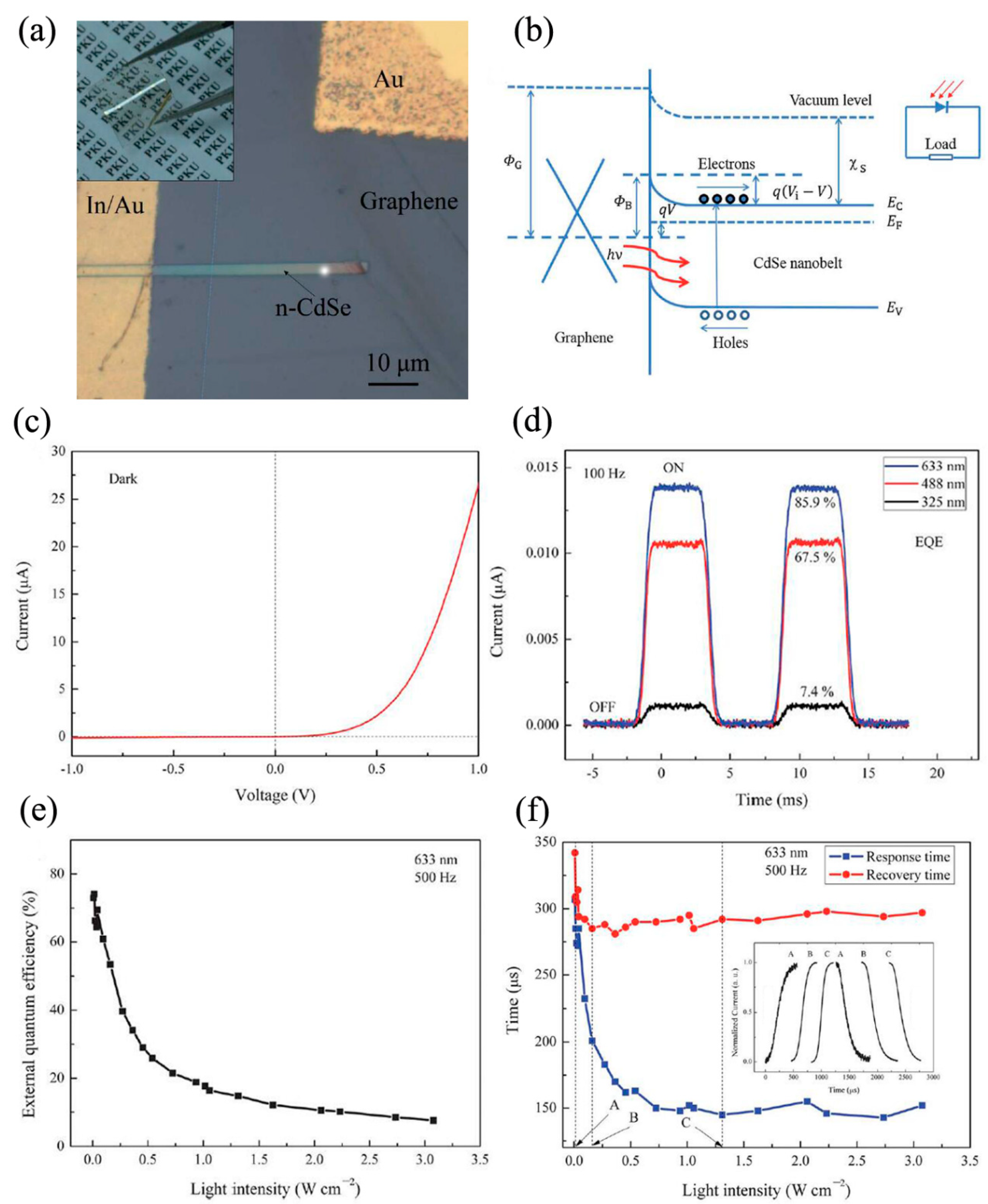
- Jin, W.; Ye, Y.; Gan, L.; Yu, B.; Wu, P.; Dai, Y.; Meng, H.; Guo, X.; Dai, L. Self-powered high performance photodetectors based on CdSe nanobelt/graphene Schottky junctions. J. Mater. Chem. 2012, 22, 2863–2867. [Google Scholar] [CrossRef]
- Xu, J.; Rechav, K.; Popovitz-Biro, R.; Nevo, I.; Feldman, Y.; Joselevich, E. High-gain 200 ns photodetectors from self-aligned CdS–CdSe core–shell nanowalls. Adv. Mater. 2018, 30, 1800413. [Google Scholar] [CrossRef] [PubMed]
- Sze, S.M.; Ng, K.K. Physics of Semiconductor Devices, 3rd ed.; Wiley: Hoboken, NJ, USA, 2007; pp. 663–668. [Google Scholar]
- Jiang, Y.; Zhang, W.J.; Jie, J.S.; Meng, X.M.; Fan, X.; Lee, S.T. Photoresponse properties of CdSe single-nanoribbon photodetectors. Adv. Funct. Mater. 2007, 17, 1795–1800. [Google Scholar] [CrossRef]
- Wu, P.; Dai, Y.; Sun, T.; Ye, Y.; Meng, H.; Fang, X.; Yu, B.; Dai, L. Impurity-dependent photoresponse properties in single CdSe nanobelt photodetectors. ACS Appl. Mater. Interfaces 2011, 3, 1859–1864. [Google Scholar] [CrossRef]
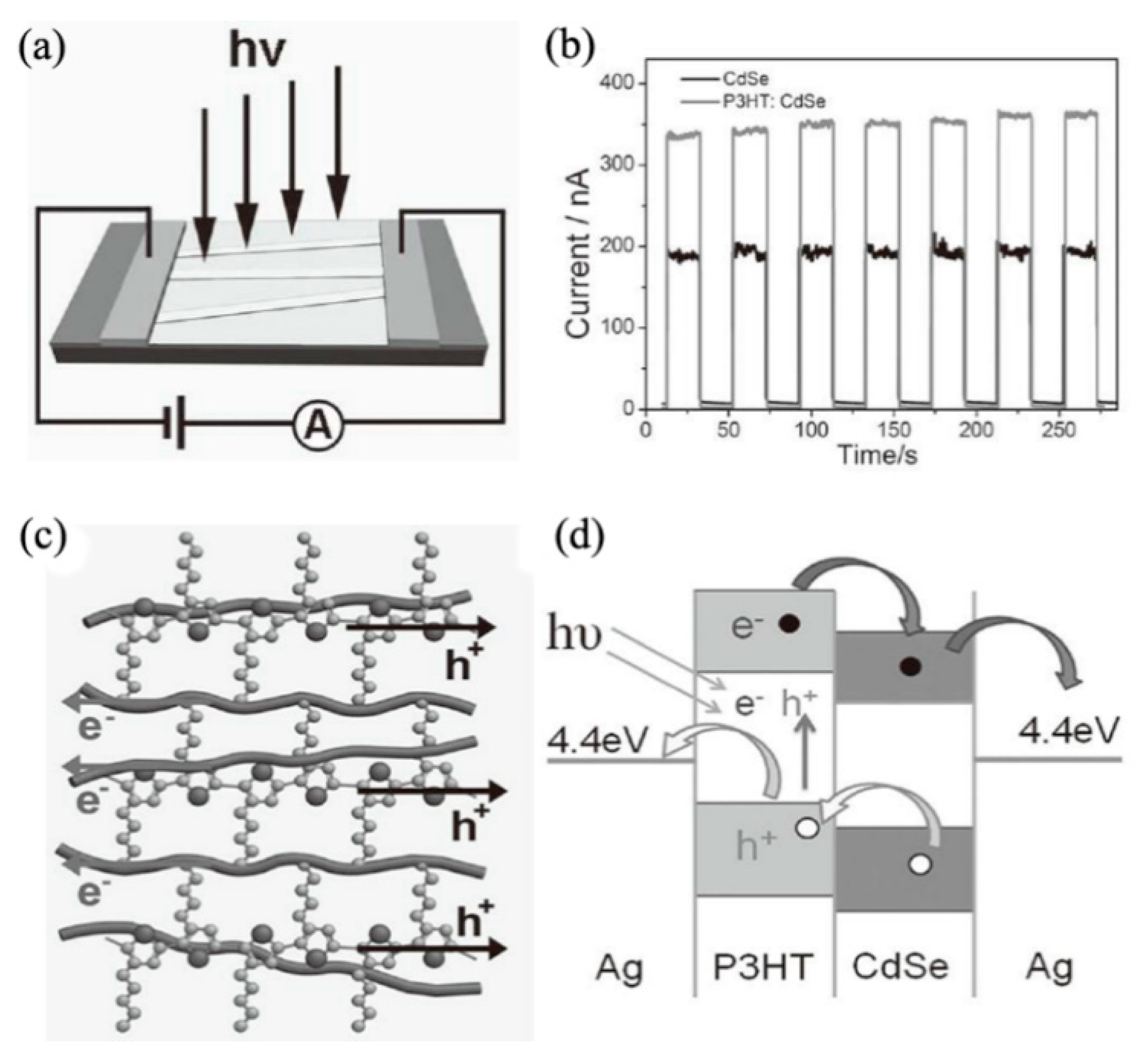
- Wang, X.; Song, W.; Liu, B.; Chen, G.; Chen, D.; Zhou, C.; Shen, G. High-performance organic-inorganic hybrid photodetectors based on P3HT: CdSe nanowire heterojunctions on rigid and flexible substrates. Adv. Funct. Mater. 2013, 23, 1202–1209. [Google Scholar] [CrossRef]
- Chen, G.; Liu, Z.; Liang, B.; Yu, G.; Xie, Z.; Huang, H.; Liu, B.; Wang, X.; Chen, D.; Zhu, M.Q.; et al. Single-crystalline p-Type Zn3As2 nanowires for field-effect transistors and visible-light photodetectors on rigid and flexible substrates. Adv. Funct. Mater. 2013, 23, 2681–2690. [Google Scholar] [CrossRef]
- Chand, N.; Houston, P.A.; Robson, P.N. Gain of a heterojunction bipolar phototransistor. IEEE Trans. Electron. Devices 1985, 32, 622–627. [Google Scholar] [CrossRef]
- Hu, C.; Dong, D.; Yang, X.; Qiao, K.; Yang, D.; Deng, H.; Yuan, S.; Khan, J.; Lan, Y.; Song, H.; et al. Synergistic effect of hybrid PbS quantum dots/2D-WSe2 toward high performance and broadband phototransistors. Adv. Funct. Mater. 2017, 27, 1603605. [Google Scholar] [CrossRef]
- Island, J.O.; Blanter, S.I.; Buscema, M.; van der Zant, H.S.J.; Castellanos-Gomez, A. Gate controlled photocurrent generation mechanisms in high-gain In2Se3 phototransistors. Nano Lett. 2015, 15, 7853–7858. [Google Scholar] [CrossRef] [PubMed]
- Guo, Q.; Pospischil, A.; Bhuiyan, M.; Jiang, H.; Tian, H.; Farmer, D.; Deng, B.; Li, C.; Han, S.-J.; Wang, H.; et al. Black phosphorus mid-infrared photodetectors with high gain. Nano Lett. 2016, 16, 4648–4655. [Google Scholar] [CrossRef] [PubMed]
- An, X.; Liu, F.; Jung, Y.J.; Kar, S. Tunable graphene–silicon heterojunctions for ultrasensitive photodetection. Nano Lett. 2013, 13, 909–916. [Google Scholar] [CrossRef] [PubMed]
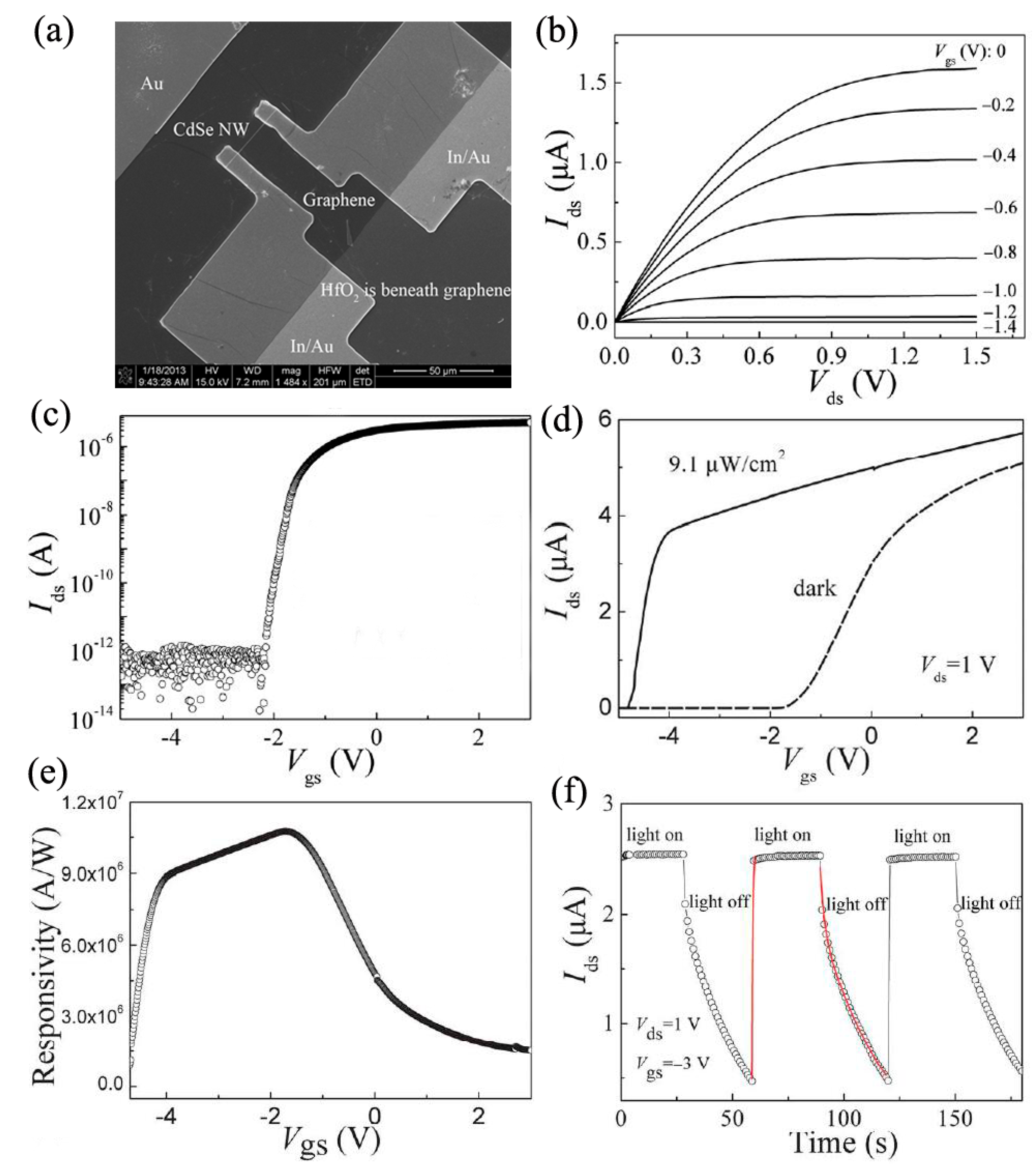
- Dai, Y.; Yu, B.; Ye, Y.; Wu, P.; Meng, H.; Dai, L.; Qin, G. High-performance CdSe nanobelt based MESFETs and their application in photodetection. J. Mater. Chem. 2012, 22, 18442–18446. [Google Scholar] [CrossRef]
- Dong, Y.; Gu, Y.; Zou, Y.; Song, J.; Xu, L.; Li, J.; Xue, J.; Li, X.; Zeng, H. Improving all-inorganic perovskite photodetectors by preferred orientation and plasmonic effect. Small 2016, 12, 5622–5632. [Google Scholar] [CrossRef] [PubMed]
- Gogurla, N.; Sinha, A.K.; Santra, S.; Manna, S.; Ray, S.K. Multifunctional Au-ZnO plasmonic nanostructures for enhanced UV photodetector and room temperature NO sensing devices. Sci. Rep. 2014, 4, 6483. [Google Scholar] [CrossRef]
- Lu, J.; Xu, C.; Dai, J.; Li, J.; Wang, Y.; Lin, Y.; Li, P. Improved UV photoresponse of ZnO nanorod arrays by resonant coupling with surface plasmons of Al nanoparticles. Nanoscale 2015, 7, 3396–3403. [Google Scholar] [CrossRef]
- Luo, L.B.; Xie, W.J.; Zou, Y.F.; Yu, Y.Q.; Liang, F.X.; Huang, Z.J.; Zhou, K.Y. Surface plasmon propelled high-performance CdSe nanoribbons photodetector. Opt. Express 2015, 23, 12979–12988. [Google Scholar] [CrossRef]
- Gu, F.; Wang, P.; Yu, H.; Guo, B.; Tong, L. Optical quenching of photoconductivity in CdSe single nanowires via waveguiding excitation. Opt. Express 2011, 19, 10880–10885. [Google Scholar] [CrossRef]
- Chen, J.; Lourette, S.; Rezai, K.; Hoelzer, T.; Lake, M.; Nesladek, M.; Bouchard, L.S.; Hemmer, P.; Budker, D. Optical quenching and recovery of photoconductivity in single-crystal diamond. Appl. Phys. Lett. 2017, 110, 011108. [Google Scholar] [CrossRef]
- Cai, S.; Parish, G.; Umana-Membreno, G.A.; Dell, J.M.; Nener, B.D. Optical quenching of photoconductivity in undoped n-GaN. J. Appl. Phys. 2004, 95, 1081–1088. [Google Scholar] [CrossRef]
- Peng, M.; Liu, Y.; Yu, A.; Zhang, Y.; Liu, C.; Liu, J.; Wu, W.; Zhang, K.; Shi, X.; Kou, J.; et al. Flexible self-powered GaN ultraviolet photoswitch with piezo-phototronic effect enhanced on/off ratio. ACS Nano 2016, 10, 1572–1579. [Google Scholar] [CrossRef]
- Lin, P.; Zhu, L.; Li, D.; Xu, L.; Pan, C.; Wang, Z. Piezo-phototronic effect for enhanced flexible MoS2/WSe2 van der Waals photodiodes. Adv. Funct. Mater. 2018, 28, 1802849. [Google Scholar] [CrossRef]
- Rai, S.C.; Wang, K.; Chen, J.; Marmon, J.K.; Bhatt, M.; Wozny, S.; Zhang, Y.; Zhou, W. Enhanced broad band photodetection through piezo-phototronic effect in CdSe/ZnTe core/shell nanowire array. Adv. Electron. Mater. 2015, 1, 1400050. [Google Scholar] [CrossRef]
- Yu, X.-X.; Yin, H.; Li, H.X.; Zhang, W.; Zhao, H.; Li, C.; Zhu, M.Q. Piezo-phototronic effect modulated self-powered UV/visible/near-infrared photodetectors based on CdS: P3HT microwires. Nano Energy 2017, 34, 155–163. [Google Scholar] [CrossRef]
- Dong, L.; Niu, S.; Pan, C.; Yu, R.; Zhang, Y.; Wang, Z.L. Piezo-phototronic effect of CdSe nanowires. Adv. Mater. 2012, 24, 5470–5475. [Google Scholar] [CrossRef]
- Rai, S.C.; Wang, K.; Ding, Y.; Marmon, J.K.; Bhatt, M.; Zhang, Y.; Zhou, W.; Wang, Z.L. Piezo-phototronic effect enhanced UV/visible photodetector based on fully wide band gap type-II ZnO/ZnS core/shell nanowire array. ACS Nano 2015, 9, 6419–6427. [Google Scholar] [CrossRef]
- Peng, W.; Wang, X.; Yu, R.; Dai, Y.; Zou, H.; Wang, A.C.; He, Y.; Wang, Z.L. Enhanced performance of a self-powered organic/inorganic photodetector by pyro-phototronic and piezo-phototronic effects. Adv. Mater. 2017, 29, 1606698. [Google Scholar] [CrossRef]
- Han, X.; Du, W.; Yu, R.; Pan, C.; Wang, Z.L. Piezo-phototronic enhanced UV sensing based on a nanowire photodetector array. Adv. Mater. 2015, 27, 7963–7969. [Google Scholar] [CrossRef] [PubMed]
- Huang, Y.; Duan, X.; Wei, Q.; Lieber, C.M. Directed assembly of one-dimensional nanostructures into functional networks. Science 2001, 291, 630. [Google Scholar] [CrossRef] [PubMed]
- Long, Y.Z.; Yu, M.; Sun, B.; Gu, C.Z.; Fan, Z. Recent advances in large-scale assembly of semiconducting inorganic nanowires and nanofibers for electronics, sensors and photovoltaics. Chem. Soc. Rev. 2012, 41, 4560–4580. [Google Scholar] [CrossRef] [PubMed]
- Zhou, R.; Chang, H.C.; Protasenko, V.; Kuno, M.; Singh, A.K.; Jena, D.; Xing, H. CdSe nanowires with illumination-enhanced conductivity: Induced dipoles, dielectrophoretic assembly, and field-sensitive emission. J. Appl. Phys. 2007, 101, 073704. [Google Scholar] [CrossRef]
- Li, M.; Bhiladvala, R.B.; Morrow, T.J.; Sioss, J.A.; Lew, K.K.; Redwing, J.M.; Keating, C.D.; Mayer, T.S. Bottom-up assembly of large-area nanowire resonator arrays. Nature Nanotech. 2008, 3, 88. [Google Scholar] [CrossRef] [PubMed]
- Fan, Z.; Ho, J.C.; Jacobson, Z.A.; Yerushalmi, R.; Alley, R.L.; Razavi, H.; Javey, A. Wafer-scale assembly of highly ordered semiconductor nanowire arrays by contact printing. Nano Lett. 2008, 8, 20–25. [Google Scholar] [CrossRef] [PubMed]
- Tang, J.; Sargent, E.H. Infrared colloidal quantum dots for photovoltaics: Fundamentals and recent progress. Adv. Mater. 2011, 23, 12–29. [Google Scholar] [CrossRef]
- Choi, J.; Kim, I.; Jabbour, G.E. Enhanced surface passivation of colloidal CdSe nanocrystals for improved efficiency of nanocrystal/polymer hybrid solar cells. IEEE J. Photovolt. 2016, 6, 1203–1209. [Google Scholar] [CrossRef]
- Morgan, D.P.; Kelley, D.F. Mechanism of hole trap passivation in CdSe quantum dots by alkylamines. J. Phys. Chem. C 2018, 122, 25661–25667. [Google Scholar] [CrossRef]
- Wang, J.; Fang, H.; Wang, X.; Chen, X.; Lu, W.; Hu, W. Recent Progress on localized field enhanced two-dimensional material photodetectors from ultraviolet—Visible to infrared. Small 2017, 13, 1700894. [Google Scholar] [CrossRef]
- Fang, H.; Hu, W. Photogating in low dimensional photodetectors. Adv. Sci. 2017, 4, 1700323. [Google Scholar] [CrossRef] [PubMed]


© 2019 by the authors. Licensee MDPI, Basel, Switzerland. This article is an open access article distributed under the terms and conditions of the Creative Commons Attribution (CC BY) license (http://creativecommons.org/licenses/by/4.0/).
Share and Cite
Jin, W.; Hu, L. Review on Quasi One-Dimensional CdSe Nanomaterials: Synthesis and Application in Photodetectors. Nanomaterials 2019, 9, 1359. https://doi.org/10.3390/nano9101359
Jin W, Hu L. Review on Quasi One-Dimensional CdSe Nanomaterials: Synthesis and Application in Photodetectors. Nanomaterials. 2019; 9(10):1359. https://doi.org/10.3390/nano9101359
Chicago/Turabian StyleJin, Weifeng, and Luodan Hu. 2019. "Review on Quasi One-Dimensional CdSe Nanomaterials: Synthesis and Application in Photodetectors" Nanomaterials 9, no. 10: 1359. https://doi.org/10.3390/nano9101359
APA StyleJin, W., & Hu, L. (2019). Review on Quasi One-Dimensional CdSe Nanomaterials: Synthesis and Application in Photodetectors. Nanomaterials, 9(10), 1359. https://doi.org/10.3390/nano9101359