Article

Fabrication and Characterization of AlGaN-Based UV LEDs with a ITO/Ga2O3/Ag/Ga2O3 Transparent Conductive Electrode

1
Engineering Research Center for Optoelectronics of Guangdong Province, School of Electronics and Information Engineering, South China University of Technology, Guangzhou 510640, China
2
School of Physics and Optoelectronics, South China university of Technology, Guangzhou 510640, China
3
Zhongshan Institute of Modern Industrial Technology, South China University of Technology, Zhongshan 528437, China
*
Author to whom correspondence should be addressed.
Nanomaterials 2019, 9(1), 66; https://doi.org/10.3390/nano9010066
Submission received: 30 November 2018 / Revised: 27 December 2018 / Accepted: 31 December 2018 / Published: 5 January 2019
(This article belongs to the Special Issue Optoelectronic Nanodevices)

Abstract

:
We fabricated a complex transparent conductive electrode (TCE) based on Ga2O3 for AlGaN-based ultraviolet light-emitting diodes. The complex TCE consists of a 10 nm ITO, a 15 nm Ga2O3, a 7 nm Ag, and a 15 nm Ga2O3, forming a ITO/Ga2O3/Ag/Ga2O3 multilayer. The metal layer embedded into Ga2O3 and the thin ITO contact layer improves current spreading and electrode contact properties. It is found that the ITO/Ga2O3/Ag/Ga2O3 multilayer can reach a 92.8% transmittance at 365 nm and a specific contact resistance of 10−3 Ω·cm2 with suitable annealing conditions.

1. Introduction

AlGaN-based ultraviolet (UV) light-emitting diodes (LEDs) can achieve the full wavelength coverage of UVA (400–320 nm), UVB (320–280 nm) and UVC (280–200 nm) by changing Al content. As a result, AlGaN-based UV LEDs have attracted considerable attention and are seen as a promising lighting source for different applications in environmental cleaning, medicine, printing, microscopy and lighting [1,2,3,4,5,6]. However, the external quantum efficiency (EQE) of AlGaN-based UV LEDs is still much lower than that of the commercially available blue LEDs with an EQE close to 20% for UVA and <1% for UVC devices [7,8,9]. This phenomenon obstructs commercial applications of the AlGaN-based UV LEDs. Indium tin oxide (ITO) is widely used as transparent contact layers in traditional GaN-based blue and green LEDs. However, there is serious light absorption in the ITO in the ultraviolet band due to the band gap of ITO ranging from 3.5 eV to 4.3 eV [10,11]. Previous studies reported that doping metals in ITO would reduce the light absorption in near UV LEDs. The transmittance of ITO at wavelengths above 380 nm can reach about 90% by optimizing the thickness of metal and the annealing temperature [12,13,14,15]. But the transmittance of ITO still decreases rapidly when the wavelength becomes shorter. Thus, it is very urgent for a layer with higher transmittance in ultraviolet band to be able to replace the traditional ITO transparent conductive electrode (TCE) in UV LEDs.
Ga2O3, which has a bandgap from 4.9 eV to 5 eV, is an attractive alternative for TCE in UV LEDs because of its high transmittance in UV band [16,17,18]. In addition, a large size and high quality Ga2O3 thin film can be fabricated by single crystals synthesized by the melt growth method [19]. This material has been studied in the fields of metal semiconductor field effect transistors, metal oxide semiconductor field effect transistors and Schottky barrier diodes. However, the conductivity of Ga2O3 is very poor. Many approaches have been developed to promote the conductivity of Ga2O3. Orita Mi Hiramatsu H et al. improved the conductivity of β-Ga2O3 by doping In or Sn into Ga2O3 [16]. The (201)-oriented Sn-doped β-Ga2O3 films obtained a maximum conductivity of 8.2 S/cm (about 1.22 × 10⁴ Ω/sq). But it is still too low to be used as TCE in UV LED. Liu JJ et al. grew ITO thin films in Ga2O3 films and improved the sheet resistance and transmittance of Ga2O3/ITO films by adjusting the growth temperature and the thickness of ITO [17]. A sheet resistance of 323 Ω/sq and a transmittance at 280 nm of 77.6% can be achieved. Jae-kwan Kim et al. realized that the transmittance at 380 nm is 80.944% and the sheet resistance is 58.6 Ω/sq [20]. The Kie Young Woo group in Korea prepared the Ag/Ga2O3 model by learning the ITO/Ag/ITO model [21]. The contact characteristics and conductivity of the Ga2O3 films were improved by the Ag intercalation layer, and the transmittance at 380 nm and specific contact resistivity of the Ag/Ga2O3 thin film were 91% and 3.06 × 10⁻² Ω·cm2 respectively.
In this paper, a complex TCE based on Ga2O3 is proposed to enhance the efficiency of UV LEDs. We prepared the complex Ga2O3-based TCE by depositing an ITO contact layer, a Ga2O3 layer, an Ag metal intercalation layer and another Ga2O3 layer in sequence, forming an ITO/Ga2O3/Ag/Ga2O3 multilayer. The resistance and transmittance ITO/Ga2O3/Ag/Ga2O3 multilayer with a different annealing temperature were studied and analyzed systematically. The sheet resistance of the ITO/Ga2O3/Ag/Ga2O3 multilayer was detected by four-point probe methods. The optical transmittance was measured by a UV/visible spectrophotometer. The surface roughness of these ITO/Ga2O3/Ag/Ga2O3 multilayer were measured by atomic force microscope (AFM). The X-ray photoelectron spectroscopy (XPS) and Auger electron spectroscopy (AES) measurements were also used to analyze the ITO/Ga2O3/Ag/Ga2O3 multilayer. Furthermore, we employed the ITO/Ga2O3/Ag/Ga2O3 multilayer as TCEs on 365 nm UV epitaxy in comparison to those with conventional ITO.

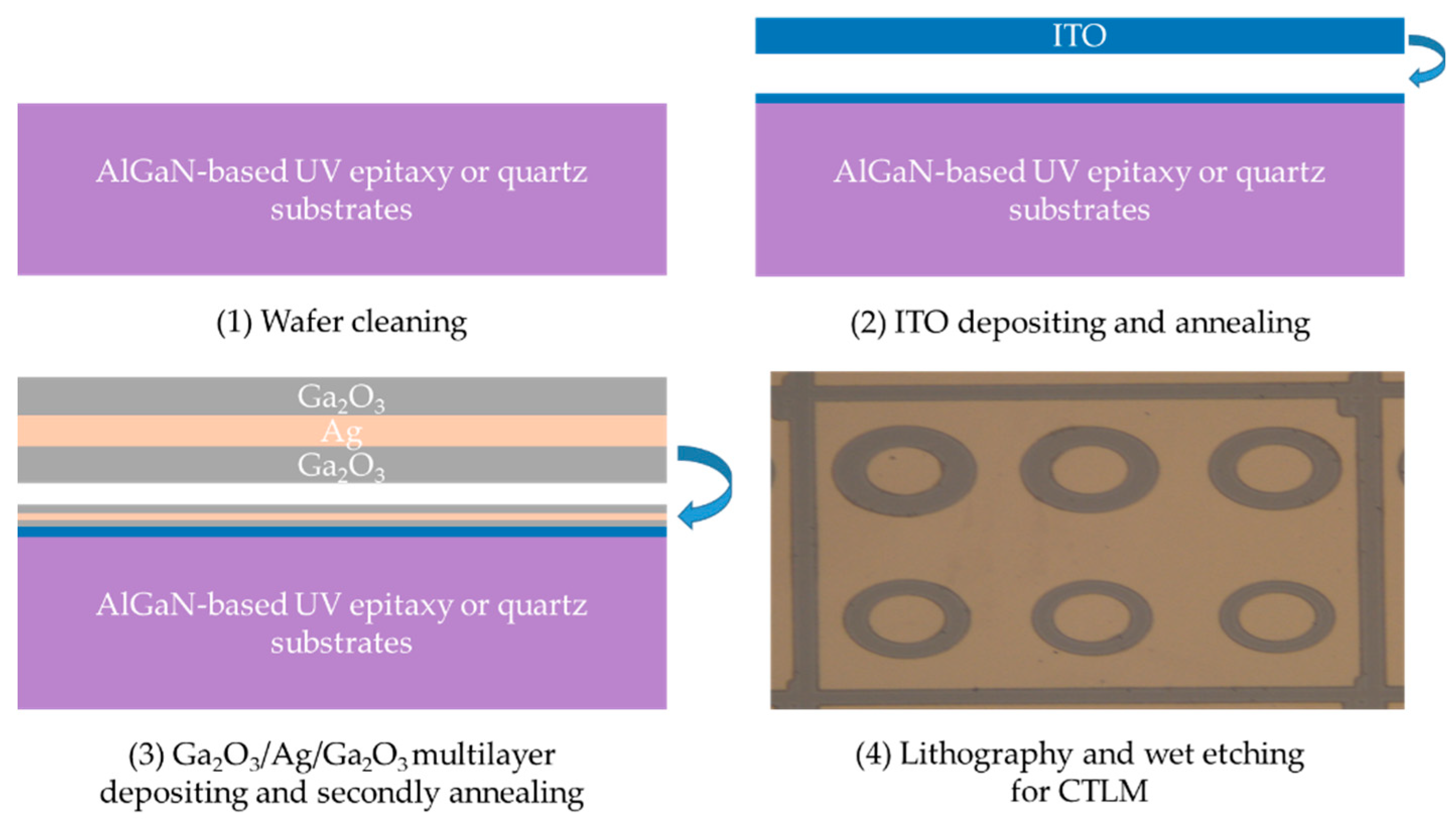
2. Materials and Methods
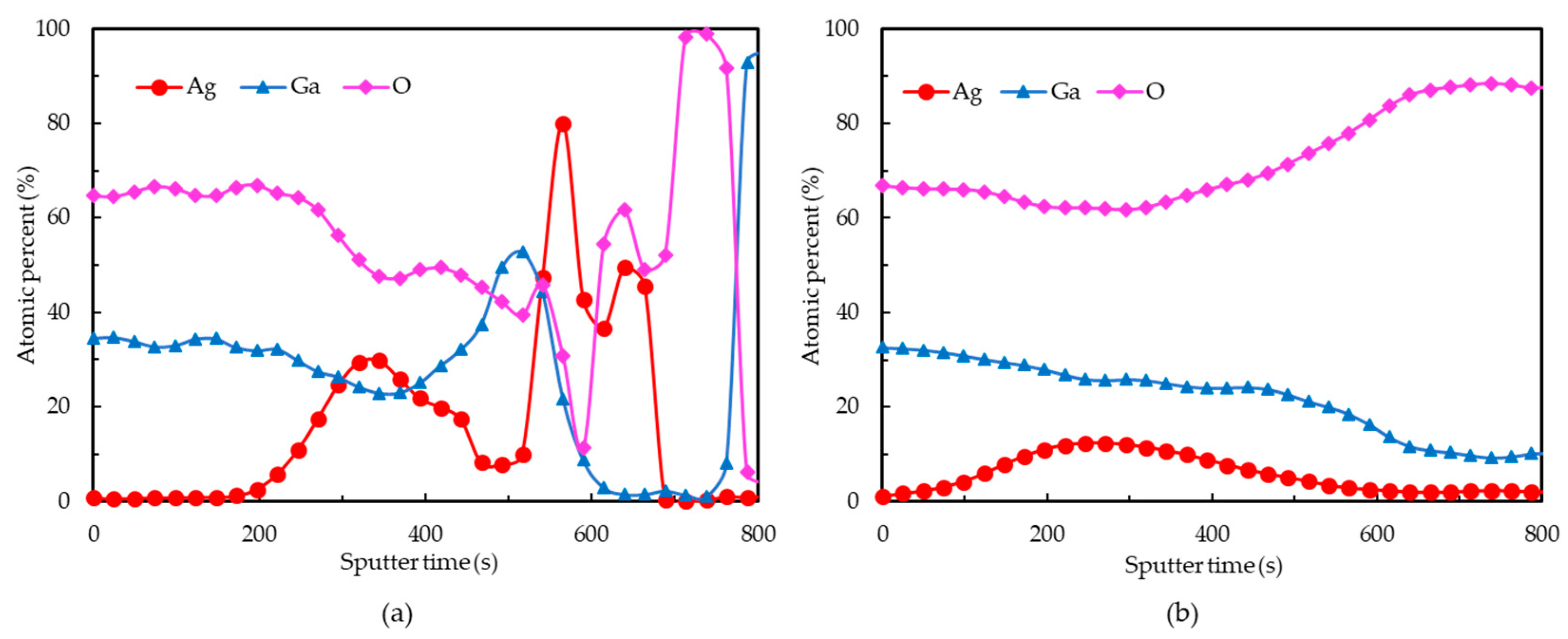
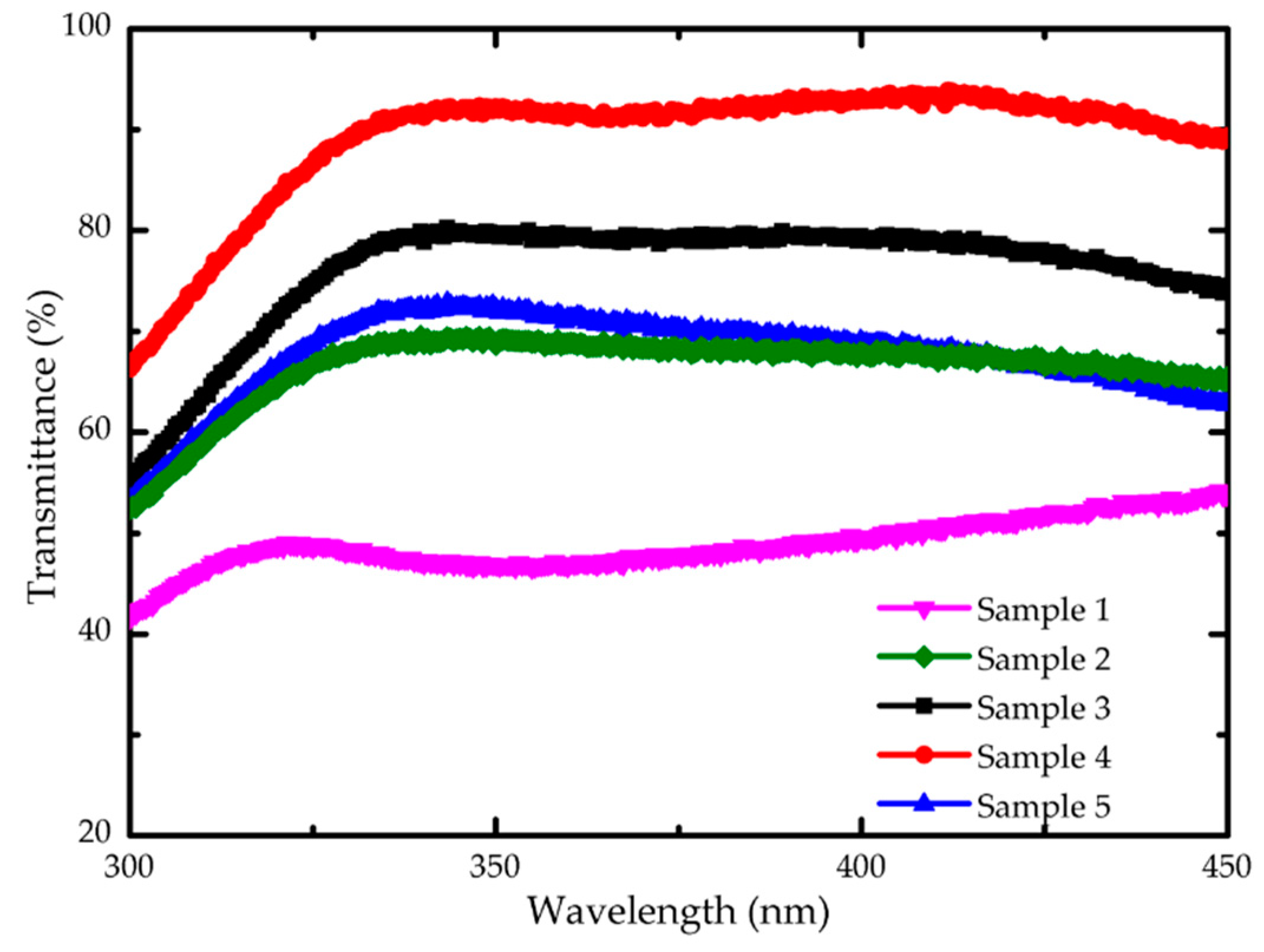
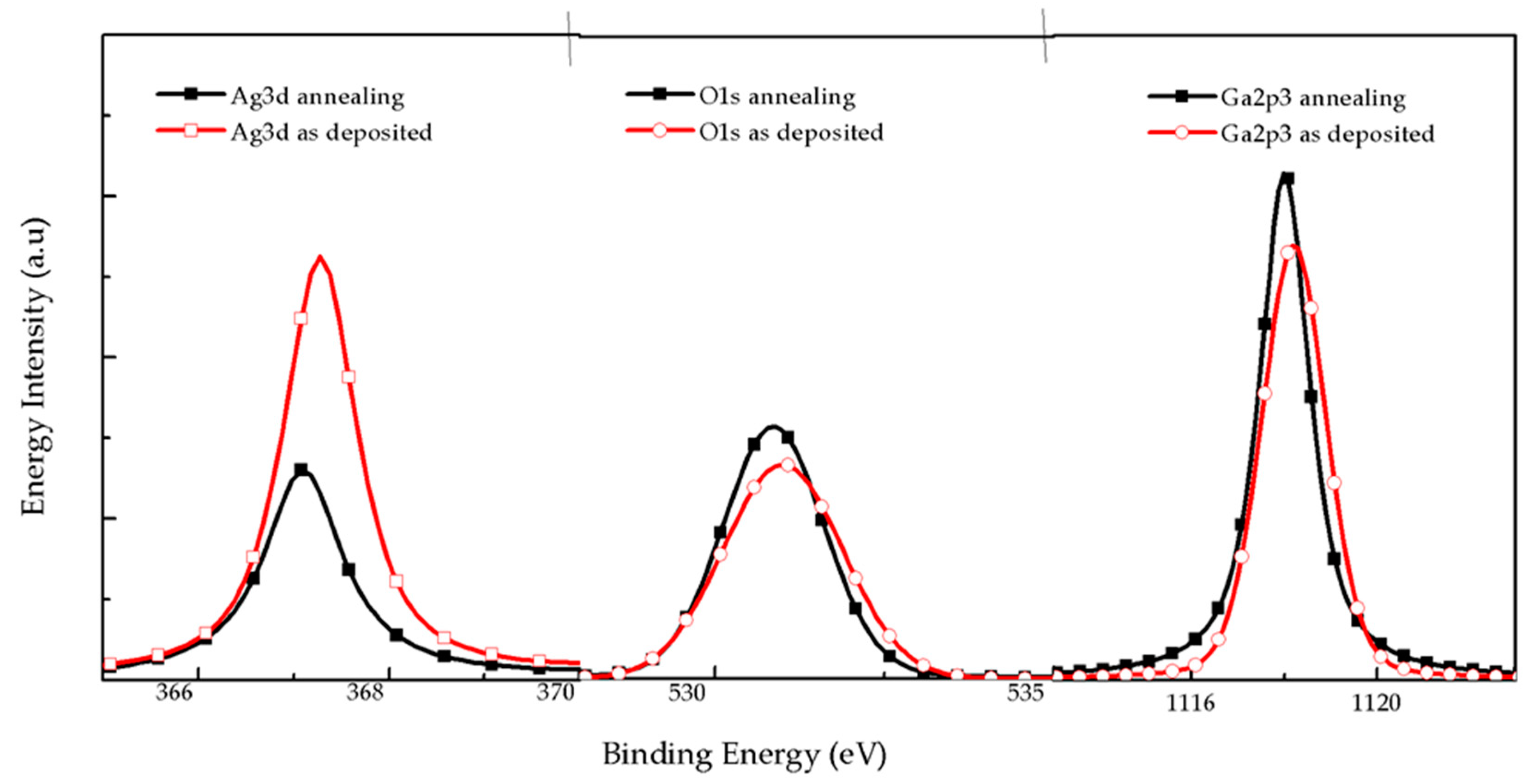
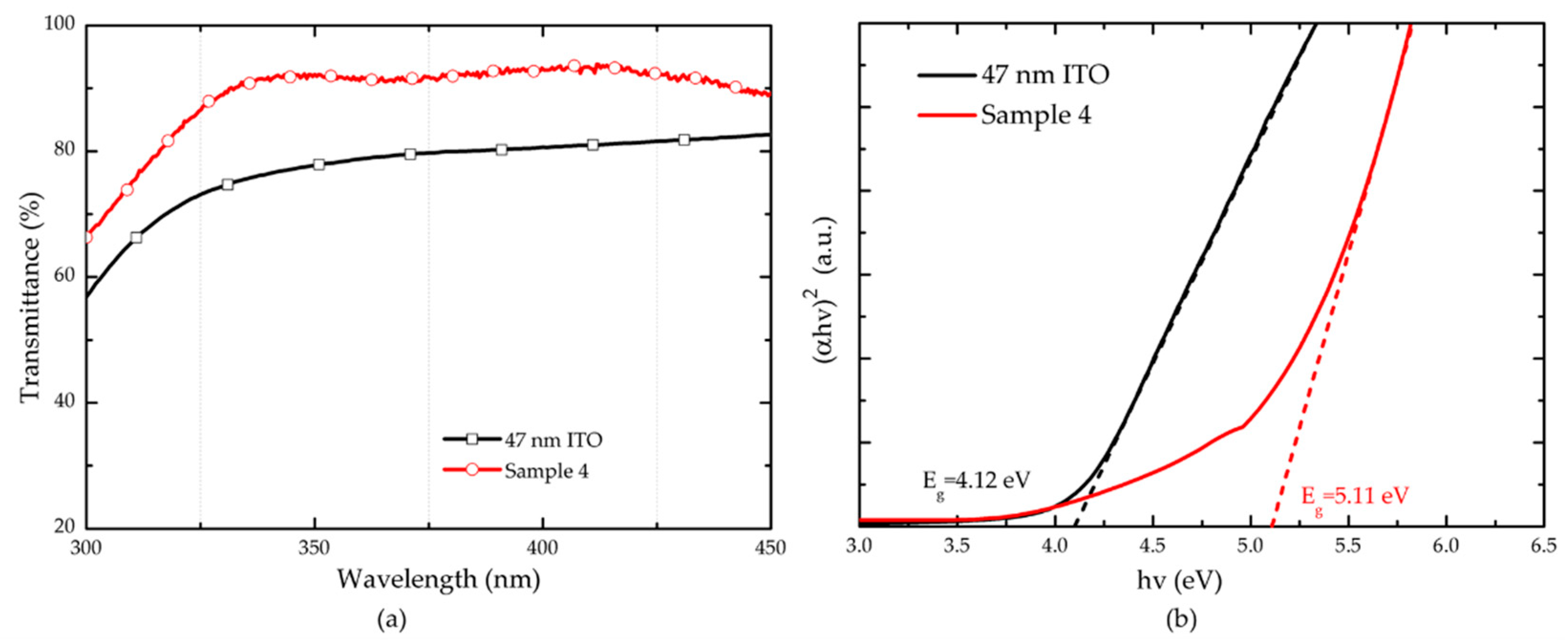
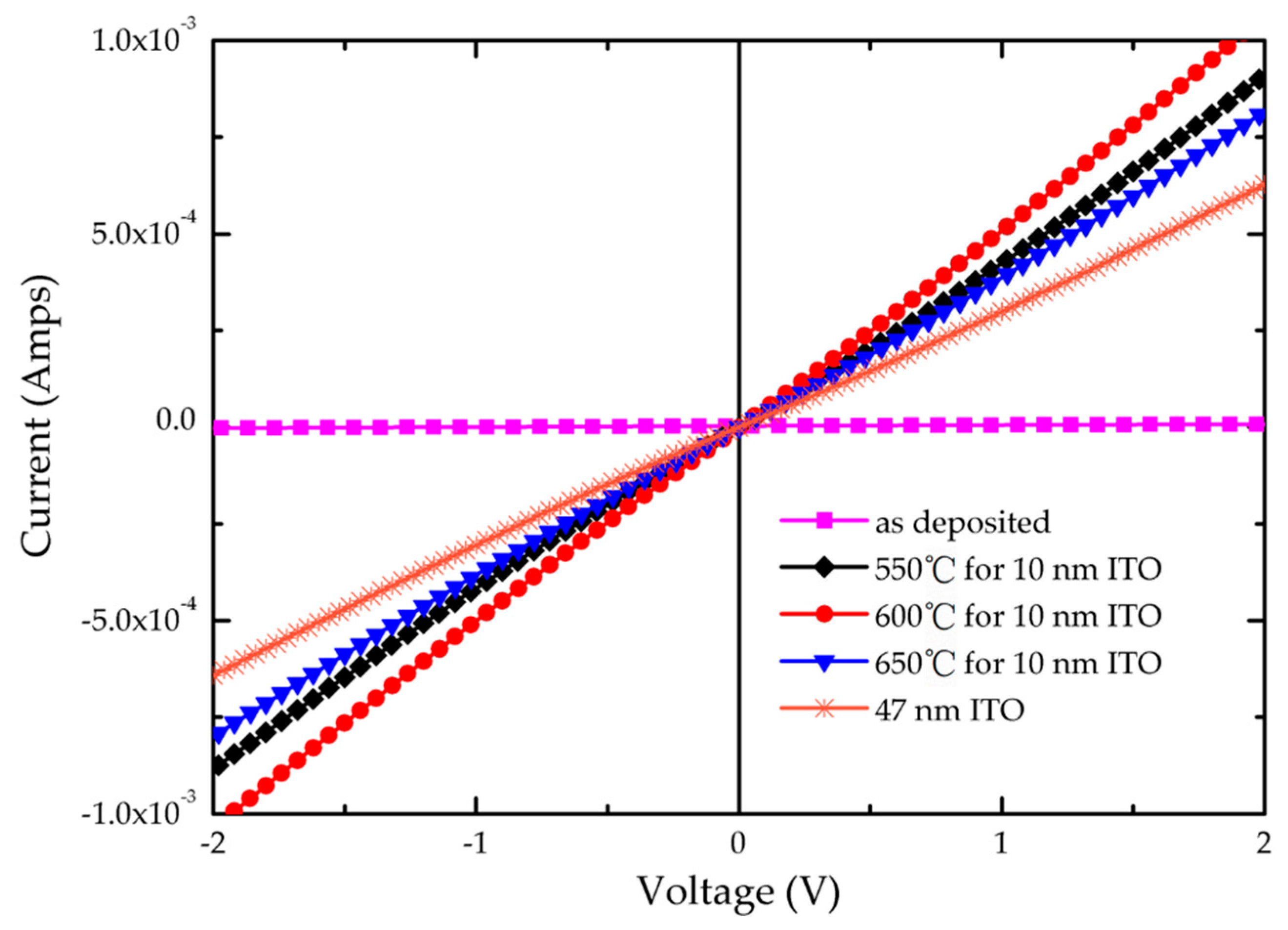
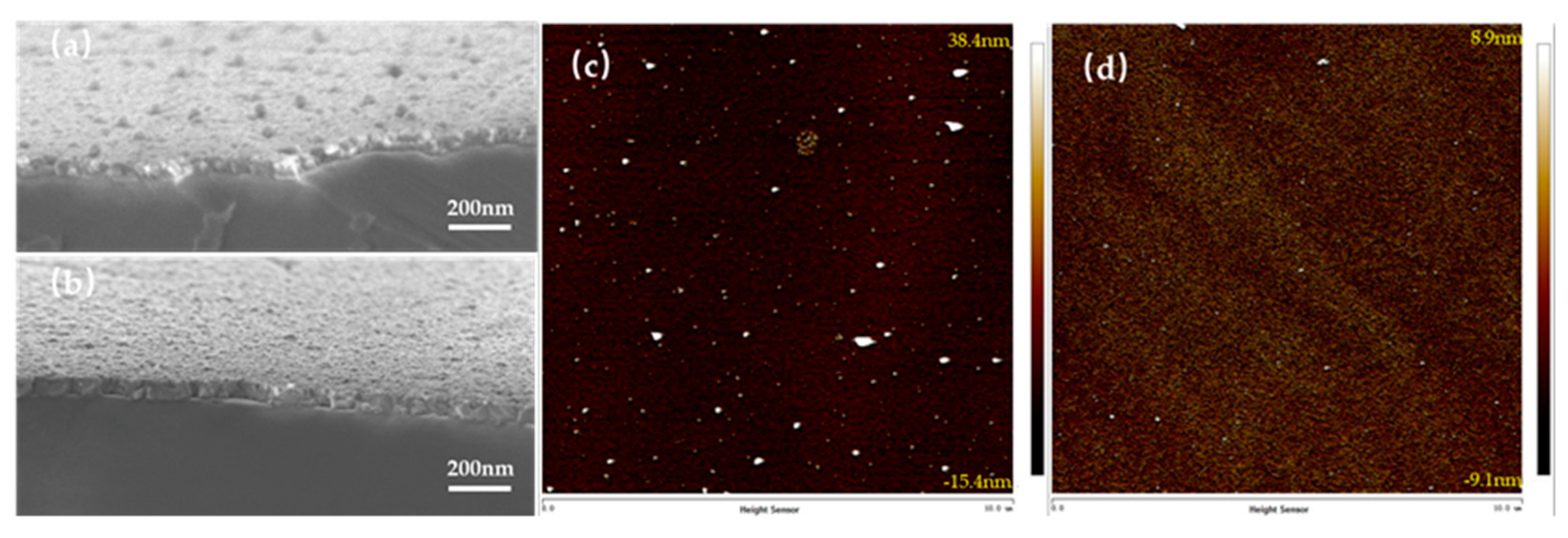
To investigate the influence of a Ag intercalation layer on the Ga2O3 layer, a Ga2O3/Ag/Ga2O3 (15 nm/7 nm/15 nm) multilayer was deposited on quartz substrates and then annealed at different conditions. The quartz substrates were first washed in acetone, isopropanol and deionized water and dried by nitrogen. After that, Ga2O3, Ag and Ga2O3 were sequentially deposited on the quartz substrates in magnetron sputtering equipment. In order to reduce the resistivity of the Ga2O3 layer but not affect its transmittance, the thickness of the Ag embedding interlayer and Ga2O3 were set to be 7 nm and 15 nm respectively. The Ga2O3 thin films were all deposited by RF magnetron sputtering of Ga2O3 (purity 99.99%) ceramic target, and the Ag thin film was deposited by direct current magnetron sputtering of the Ag target. The sputtering cavity was pumped to 5 × 10⁻⁶ Pa before the sputtering begin. The sputtering atmosphere was pure argon with the pressure of 5 mtorr. The rotation speed of the cavity substrate is 20 rpm. The temperature was controlled at about 35 °C ± 1 °C by feedback control heater during deposition. Afterwards, all the Ga2O3/Ag/Ga2O3 multilayer samples were annealed by a rapid thermal annealing (RTA) system at a different temperature and ambient. We used X-ray photoelectron spectroscopy (XPS) and Auger electron spectroscopy (AES) to analyze the element diffusion effect of the Ga2O3/Ag/Ga2O3 multilayer.
To further improve the contact between Ga2O3 and AlGaN-based UV epitaxy, we insert an ITO thin film below the Ga2O3/Ag/Ga2O3 multilayer as a contact layer. We prepared ITO/Ga2O3/Ag/Ga2O3 multilayer on quartz substrates. Before the deposition of Ga2O3/Ag/Ga2O3 multilayer, a 10 nm ITO was deposited on quartz substrates by RF magnetron sputtering of ITO (In2O3: 90 wt%, SnO2: 10 wt%) and then annealed by RTA. Subsequently, Ga2O3/Ag/Ga2O3 multilayer was deposited on the annealed ITO thin films and the whole ITO/Ga2O3/Ag/Ga2O3 multilayer was annealed again.
Finally, we prepared ITO/Ga2O3/Ag/Ga2O3 multilayer on AlGaN-based UV epitaxy in the same method to study the specific contact resistance through the CTLM model. A 47 nm ITO thin film on quartz substrates and epitaxy was also prepared as reference, which was annealed at 600 °C for 1 min in a mixture of N2/O2 (200 sccm:35 sccm) ambient. The procedures of ITO/Ga2O3/Ag/Ga2O3 multilayer and optical micrograph of contact surface on CTLM patterns are shown in Figure 1.

3. Results

In order to study the influence of annealing conditions on the sheet resistance of Ga2O3/Ag/Ga2O3 multilayer, a series of Ga2O3/Ag/Ga2O3 multilayer on quartz substrates were annealed at different temperature and ambient. The annealing temperature changed from 400 °C to 600 °C with the annealing ambient changing from N2/O2 mixture and pure O2 ambient. As shown in Table 1, the sheet resistance increases with the decrease of annealing temperature. It is found that the Ga2O3/Ag/Ga2O3 multilayer could reach the lowest sheet resistance of 16.45 Ω/sq after being annealed at 600 °C for 1 min in an N2/O2 mixture ambient. The result means that the effect of Ag as the insertion layer is not obvious at low temperature, and the metal diffusion reaction is not sufficient. The metal insertion layer in the film can fully diffuse to the Ga2O3 layer and decrease the resistance value of the Ga2O3/Ag/Ga2O3 multilayer when the temperature reaches 600 °C. The resistance of the multilayer annealed at 600 °C in pure oxygen ambient is higher than that of the multilayer in an N2/O2 mixture annealing ambient. Besides, the higher the oxygen ratio in the annealing atmosphere, the higher the multilayer resistance value becomes. The reason for this is that metal oxides form and then affect the resistance of film [22,23].
Figure 2 and Table 2 show the XPS energy spectral of Ga2O3/Ag/Ga2O3 multilayer on quartz substrate before and after annealing at 600 °C for 1 min in N2/O2 mixture ambient. The energy intensity, peak value quantum-number vertex, high half-width and atomic fraction content of Ag3d, O1s, Ga2p3 were measured at the depth of about 10 nm of the multilayer. The open symbol and solid symbol in Figure 2 represent the energy intensity of the elements before and after annealing respectively. We can see that the energy value of element Ag3d is high, the quantum number per second is 13581 states/s, and the atomic fraction is 0.47 before annealing. After annealing, the energy intensity and the atomic ratio of Ag atom decrease relatively, which is 6651.8 counts/s and 0.29%, respectively. The energy and atomic ratio of Ga and O increase a little after annealing. The decrease of atomic ratio of Ag atom means that the process of annealing results in diffusion of Ag in the multilayer. Therefore, the sheet resistance of annealed Ga2O3/Ag/Ga2O3 multilayer decreases compared to that of the as-deposited sample due to the diffusion of internal elements.
In addition, to further identify the distribution of composition in Ga2O3/Ag/Ga2O3 multilayer, we analyzed the Ga2O3/Ag/Ga2O3 multilayer on quartz substrate using AES measurement. Figure 3 shows the AES depth profiles of the Ga2O3/Ag/Ga2O3 multilayer before and after annealing at 600 °C for 1 min in N2/O2 mixture ambient. For the multilayer before annealing, the atomic percent of Ag is low in the surface and increases after a specific sputter time, which means that the Ag do not diffuse into the multilayer. Since the Ga2O3 and quartz substrates have poor conductivity, the atomic percent will become random and fluctuant due to the charge accumulation effect when the sputter time increases. By contrast, the atomic percent of Ag increases at the beginning of sputtering and the Ag atoms distribute more evenly in the whole multilayer after annealing as shown in Figure 3b. This result demonstrates that the Ag will diffuses into the Ga2O3 layer during the annealing process, leading to the reduction of sheet resistance of the Ga2O3/Ag/Ga2O3 multilayer.
Because of the bad contact property between Ga2O3 and p-GaN on epitaxial wafer, we insert a 10 nm ITO thin film below Ga2O3 as the contact layer. In order to optimal the transmittance and sheet resistance of the ITO/Ga2O3/Ag/Ga2O3 multilayer, we prepared five ITO/Ga2O3/Ag/Ga2O3 multilayer samples on quartz substrates and changed the annealing temperature as shown in Table 3. Among the five samples, sample 1 was not annealed. Sample 2 was annealed at 600 °C as a whole. For sample 3 to sample 5, the 10 nm ITO layer was firstly annealed at 550/600/650 °C respectively and then the whole ITO/Ga2O3/Ag/Ga2O3 multilayer were annealed at 600 °C. The annealing process of ITO and ITO/Ga2O3/Ag/Ga2O3 multilayer both maintained in N2/O2 (200 sccm:35 sccm) mixture ambient for 1 min. Figure 4 is the transmittance curves of five samples at range of 300 nm to 450 nm. It is obvious that sample 4, which was annealed at 600 °C at first and then at 600 °C again, has the highest transmittance of 92.68% at 365 nm and the lowest sheet resistance of 20.1 Ω/sq.
In addition, we compared the transmittance and sheet resistance of sample 4 and a 47 nm ITO thin film on quartz substrate. The 47 nm ITO sample was annealed at 600 °C in N2/O2 (200 sccm:35 sccm) mixture ambient for 1 min. Figure 5a plots the transmittance curves of sample 4 and 47 nm ITO. The ITO/Ga2O3/Ag/Ga2O3 multilayer demonstrates better transmittance property than 47 nm ITO especially in UV range. To further understand the origin of this result, the optical bandgap Energy Eg of sample 4 and 47 nm ITO was calculated. The Eg can be extracted from the relation between (αhv)2 and hv according to the Equations (1) and (2), as follow:
α h v = C ( h v E g ) 1 / 2
h v = h c λ i
The Eg can be obtained by extrapolating the linear (αhv)2 versus hv plots to the horizontal axis [24,25]. In Equations (1) and (2), C is a constant of direct transition, α is the light absorption coefficient, hv is the photon energy, h is Planck constant bright, c is the light speed, and λi is the wavelength [24,26,27].
If the transmittance T at each λi is known, the value of α at each λi can be obtained by Equations (3) and (4), as follow:
T = e x p ( α d )
α = L n ( 1 T ) d
where d is the thickness of films. Since we have measured the transmittance T of sample 4 and 47 nm ITO, the curves of (αhv)2 as a function of hv can be obtained as shown in Figure 5b. The optical Energy bandgap Eg of sample 4 is determined to be 4.12 eV, and that of ITO layer is 5.11 eV, by extrapolating the linear section of (αhν)2 to the hv axis. The large band gap means that the absorption of ITO/Ga2O3/Ag/Ga2O3 multilayer in UV range is smaller than that of 47 nm ITO layer. Table 4 shows the transmittance at 365 nm and sheet resistance of sample 4 and 47 nm ITO. The sample 4 has a reduction in sheet resistance compared to the 47 nm ITO sample. The transmittance of sample 4 is higher than that of 47 nm ITO and other reported metal-doped ITO [12,13,14,15]. These results reveal that the ITO/Ga2O3/Ag/Ga2O3 multilayer exhibits an advantage of transmittance at UV range and conductivity.
Finally, we prepared a series of ITO/Ga2O3/Ag/Ga2O3 multilayers on AlGaN-based UV epitaxy to study the specific contact resistance through the CTLM model. These samples were fabricated in the same process as sample 1 and sample 3, 4, 5. The 10 nm ITO contact layer was annealed at 550/600/650 °C respectively, and then the whole ITO/Ga2O3/Ag/Ga2O3 multilayer was annealed at 600 °C. The annealing process of ITO and the ITO/Ga2O3/Ag/Ga2O3 multilayer both maintained in N2/O2 (200 sccm:35 sccm) mixture ambient for 1 min. As reference, a 47 nm ITO was also deposited on epitaxy and annealed at 600 °C in N2/O2 (200 sccm:35 sccm) mixture ambient for 1 min. Figure 6 shows the Ohmic contact characteristics of annealed ITO/Ga2O3/Ag/Ga2O3 multilayer with p-GaN measured by Electroluminescence system and CTLM mode. The I–V characteristics of the as-deposited ITO/Ga2O3/Ag/Ga2O3 multilayer are insulated, because the Ga2O3 films have the properties of non-diffusion of metals, poor conductivity and insulation on the p-GaN surface. However, the multilayer whose ITO was annealed in nitrogen-oxygen atmosphere at 550 °C /600 °C /650 °C shows linear I–V characteristics on the surface of p-GaN. Also, all the annealed ITO/Ga2O3/Ag/Ga2O3 multilayers exhibit higher current compared to the 47 nm ITO on p-GaN. The slope of 600 °C annealed I-V curve is highest. The specific contact resistance of 600 °C annealed sample could reach 2.36 × 10⁻³ Ω·cm2. In contrast, the specific contact resistance of 47 nm ITO on AlGaN-based UV epitaxy is 5.68 × 10⁻³ Ω·cm2.
To further compare the differences between ITO/Ga2O3/Ag/Ga2O3 multilayer and the 47 nm ITO, we measured the surface morphology using scanning electron microscope (SEM) and AFM. The Figure 7a,b show SEM micrographs of the ITO/Ga2O3/Ag/Ga2O3 multilayer and 47 nm ITO on the AlGaN-based UV epitaxy. The surface of 47 nm ITO is smoother than that of the ITO/Ga2O3/Ag/Ga2O3 multilayer. Besides, the thickness of the multilayer is about 48 nm measured by SEM cross-section micrograph. The root-mean-square (RMS) surface roughness of the ITO/Ga2O3/Ag/Ga2O3 multilayer and 47 nm ITO on a 10 × 10 μm2 area are 6.92 nm and 2.36 nm respectively measured by AFM. A rough surface is beneficial for light emitting form chips to external. The rougher surface of the ITO/Ga2O3/Ag/Ga2O3 multilayer may be another reason for its higher transmittance.

4. Conclusions

In this paper, a complex transparent conductive electrode based on Ga2O3 for AlGaN-based UV LEDs is proposed. The complex transparent conductive electrode consists of a 10 nm ITO, a 15 nm Ga2O3, a 7 nm Ag, and a 15 nm Ga2O3, forming a ITO/Ga2O3/Ag/Ga2O3 multilayer. The ITO/Ga2O3/Ag/Ga2O3 multilayer was grown by magnetron sputtering. The resistance and transmittance ITO/Ga2O3/Ag/Ga2O3 multilayer with a different annealing temperature was studied and analyzed systematically. With suitable annealing conditions, the ITO/Ga2O3/Ag/Ga2O3 multilayer reaches a 92.8% transmittance at 365 nm and a specific contact resistance of 2.36 × 10⁻³ Ω·cm2. The XPS and AES results show that the diffusion of Ag in the multilayer leads to a low sheet resistance of the ITO/Ga2O3/Ag/Ga2O3 multilayer. The reason for the high transmittance of the ITO/Ga2O3/Ag/Ga2O3 multilayer in the UV range is the 5.11 eV band gap. These situations provide the improvement in optical characteristics of 365 nm UV LEDs. These results indicate that the proposed ITO/Ga2O3/Ag/Ga2O3 multilayer is a promising alternative for TCE to further improve the optical and electrical performances of AlGaN-based UV LED.

Author Contributions

These authors contributed equally.

Funding

This work was supported by Science and Technologies plan Projects of Guangdong Province (Nos. 2017B010112003, 2017A050506013), and by Applied Technologies Research and Development Projects of Guangdong Province (Nos. 2015B010127013, 2016B010123004), and by Science and Technologies plan Projects of Guangzhou City (Nos. 201504291502518, 201604046021, 201704030139), and by Science and Technology Development Special Fund Projects of Zhongshan City (Nos. 2017F2FC0002, 2017A1009).

Conflicts of Interest

The authors declare no conflict of interest.

References

  1. Maitland, J. UV curing of inks and coatings in digital printing applications. In Proceedings of the NIP & Digital Fabrication Conference, Baltimore, MD, USA, 18–23 September 2005. [Google Scholar]
  2. Yu, C.C.; Chuah, E.C.; Ng, Y.T.; Seah, Y.S.; Tan, P.P.; Chiu, T.H.; Hsieh, T.T. Neonatal status in cesarean section under epidural anesthesia with supplementary oxygen. Ma Zui Xue Za Zhi = Anaesthesiologica Sinica 1992, 30, 229. [Google Scholar] [PubMed]
  3. Hockberger, P.E. A history of ultraviolet photobiology for humans, animals and microorganisms. Photochem. Photobiol. 2010, 76, 561–579. [Google Scholar] [CrossRef]
  4. Schreiner, M.; Martínez-Abaigar, J.; Glaab, J.; Jansen, M. Uv-b induced secondary plant metabolites. Opt. Photonik 2014, 9, 34–37. [Google Scholar] [CrossRef]
  5. Lui, G.Y.; Roser, D.; Corkish, R.; Ashbolt, N.; Jagals, P.; Stuetz, R. Photovoltaic powered ultraviolet and visible light-emitting diodes for sustainable point-of-use disinfection of drinking waters. Sci. Total Environ. 2014, 493, 185–196. [Google Scholar] [CrossRef]
  6. Hodgkinson, J.; Tatam, R.P. Optical gas sensing: A review. Meas. Sci. Technol. 2013, 24, 012004. [Google Scholar] [CrossRef]
  7. Takano, T.; Mino, T.; Sakai, J.; Noguchi, N.; Tsubaki, K.; Hirayama, H. Deep-ultraviolet light-emitting diodes with external quantum efficiency higher than 20% at 275 nm achieved by improving light-extraction efficiency. Appl. Phys. Express 2017, 10, 031002. [Google Scholar] [CrossRef]
  8. Inoue, S.; Tamari, N.; Taniguchi, M. 150 mw deep-ultraviolet light-emitting diodes with large-area aln nanophotonic light-extraction structure emitting at 265 nm. Appl. Phys. Lett. 2017, 110, 141106. [Google Scholar] [CrossRef]
  9. Shatalov, M.; Sun, W.; Lunev, A.; Hu, X.; Dobrinsky, A.; Bilenko, Y.; Yang, J.; Shur, M.; Gaska, R.; Moe, C. Algan deep-ultraviolet light-emitting diodes with external quantum efficiency above 10%. Appl. Phys. Express 2012, 5, 2101. [Google Scholar] [CrossRef]
  10. Toyota, A.; Nakashima, N.; Sagara, T. Uv–visible transmission–absorption spectral study of au nanoparticles on a modified ito electrode at constant potentials and under potential modulation. J. Electroanal. Chem. 2004, 565, 335–342. [Google Scholar] [CrossRef]
  11. Lin, Y.H.; Liu, C.Y. Reflectivity and abnormal absorption at ito/al interface. J. Electron. Mater. 2009, 38, 108–112. [Google Scholar] [CrossRef]
  12. Lin, Y.H.; Liu, Y.S.; Liu, C.Y. Light output enhancement of near uv-led by using ti-doped ito transparent conducting layer. IEEE Photonics Technol. Lett. 2010, 22, 1443–1445. [Google Scholar] [CrossRef]
  13. Jae Hoon, L.; Kie Young, W.; Kyeong Heon, K.; Hee-Dong, K.; Tae Geun, K. Ito/ag/ito multilayer-based transparent conductive electrodes for ultraviolet light-emitting diodes. Opt. Lett. 2013, 38, 5055–5058. [Google Scholar]
  14. Kim, M.J.; Kim, T.G. Fabrication of metal-deposited indium tin oxides: Its applications to 385 nm light-emitting diodes. ACS Appl. Mater. Interfaces 2016, 8, 5453–5457. [Google Scholar] [CrossRef] [PubMed]
  15. Xu, J.; Zhang, W.; Peng, M.; Dai, J.; Chen, C. Light-extraction enhancement of gan-based 395  nm flip-chip light-emitting diodes by an al-doped ito transparent conductive electrode. Opt. Lett. 2018, 43, 2684–2687. [Google Scholar] [CrossRef] [PubMed]
  16. Orita, M.; Hiramatsu, H.; Ohta, H.; Hirano, M.; Hosono, H. Preparation of highly conductive, deep ultraviolet transparent β-ga 2 o 3 thin film at low deposition temperatures. Thin Solid Films 2002, 411, 134–139. [Google Scholar] [CrossRef]
  17. Liu, J.; Yan, J.; Shi, L.; Li, T. Semiconductor materials electrical and optical properties of deep ultraviolet transparent conductive Ga2O3/ito films by magnetron sputtering. J. Semicond. 2010, 31, 5–9. [Google Scholar]
  18. Passlack, M.; Schubert, E.F.; Hobson, W.S.; Hong, M.; Moriya, N.; Chu, S.N.G.; Konstadinidis, K.; Mannaerts, J.P.; Schnoes, M.L.; Zydzik, G.J. Ga2O3 films for electronic and optoelectronic applications. J. Appl. Phys. 1995, 77, 686–693. [Google Scholar] [CrossRef]
  19. Higashiwaki, M.; Sasaki, K.; Murakami, H.; Kumagai, Y.; Koukitu, A.; Kuramata, A.; Masui, T.; Yamakoshi, S. Recent progress in Ga2O3 power devices. Semicond. Sci. Technol. 2016, 31, 034001. [Google Scholar] [CrossRef]
  20. Kim, J.K.; Lee, J.M. Electrical and optical properties of near uv transparent conductive ito/Ga2O3 multilayer films deposited by rf magnetron sputtering. Appl. Phys. Lett. 2016, 109, 4166. [Google Scholar] [CrossRef]
  21. Woo, K.Y.; Lee, J.H.; Kim, K.H.; Kim, S.J.; Kim, T.G. Highly transparent conductive ag/Ga2O3 electrode for near-ultraviolet light-emitting diodes. Phys. Status Solidi 2015, 211, 1760–1763. [Google Scholar] [CrossRef]
  22. Wang, G.; Liu, H.; Zhao, C.; Yang, B.; Huang, X. Optical and electrical properties of annealed ito films. Acta scientiarium Naturalium Universitatis Jilinensis 1999, 4, 61–65. [Google Scholar]
  23. Cai, Q.; Cao, C.; Jiang, X.; Song, X.; Sun, Z. Microstructures and stoichiometrics of indium-tin-oxide films. Zhenkong Kexue Yu Jishu Xuebao/J. Vac. Sci. Technol. 2007, 27, 195–199. [Google Scholar]
  24. He, J.; Sun, L.; Chen, S.; Chen, Y.; Yang, P.; Chu, J. Composition dependence of structure and optical properties of cu2znsn (s, se) 4 solid solutions: An experimental study. J. Alloy. Compd. 2012, 511, 129–132. [Google Scholar] [CrossRef]
  25. Washizu, E.; Yamamoto, A.; Abe, Y.; Kawamura, M.; Sasaki, K. Optical and electrochromic properties of rf reactively sputtered wo 3 films. Solid State Ionics 2003, 165, 175–180. [Google Scholar] [CrossRef]
  26. Chandramohan, S.; Kanjilal, A.; Tripathi, J.K.; Sarangi, S.N.; Sathyamoorthy, R.; Som, T. Structural and optical properties of mn-doped cds thin films prepared by ion implantation. J. Appl. Phys. 2009, 105, 3272. [Google Scholar] [CrossRef]
  27. Lu, X.; Zhuang, Z.; Peng, Q.; Li, Y. Wurtzite cu 2 znsns 4 nanocrystals: A novel quaternary semiconductor. Chem. Commun. 2011, 47, 3141–3143. [Google Scholar] [CrossRef] [PubMed]
Figure 1. The procedures of ITO/Ga2O3/Ag/Ga2O3 multilayer and optical micrograph of contact surface on CTLM patterns.
Nanomaterials 09 00066 g001
Figure 2. XPS spectrum for Ag3d, O1s and Ga2p3 of Ga2O3/Ag/Ga2O3 multilayer on quartz substrates.
Nanomaterials 09 00066 g002
Figure 3. AES depth profiles of the Ga2O3/Ag/Ga2O3 multilayer on quartz substrates (a) before annealing and (b) after annealing.
Nanomaterials 09 00066 g003
Figure 4. The transmittance curves of ITO/Ga2O3/Ag/Ga2O3 multilayer on quartz substrates after annealing.
Nanomaterials 09 00066 g004
Figure 5. (a) Transmittance and (b) Energy bandgap of sample 4 and 47 nm ITO on quartz substrates.
Nanomaterials 09 00066 g005
Figure 6. Ohmic contact characteristics of ITO/Ga2O3/Ag/Ga2O3 multilayer with different annealing temperature for ITO contact layer.
Nanomaterials 09 00066 g006
Figure 7. The surface morphology measured by SEM and AFM. (a,c) are for ITO/Ga2O3/Ag/Ga2O3 multilayer on AlGaN-based UV epitaxy after annealing at 600 °C. (b,d) are for 47 nm ITO on AlGaN-based UV epitaxy after annealing at 600 °C.
Nanomaterials 09 00066 g007
Table 1. Sheet resistance of a Ga2O3/Ag/Ga2O3 multilayer on quartz substrates at different annealing conditions.
No.Annealing TemperatureAnnealing AmbientAnnealing TimeSheet Resistance (Ω/sq)
1As depositedAs depositedAs deposited23.86
2400 °CN2 200 sccm:O2 35 sccm1 min32.1
3500 °CN2 200 sccm:O2 35 sccm1 min27.74
4600 °CN2 200 sccm:O2 35 sccm1 min16.45
5600 °CO2 35 sccm3 min30.6
6600 °CO2 100 sccm1 min40.93
Table 2. XPS data of Ga2O3/Ag/Ga2O3 multilayer on quartz substrates.
NameAs DepositedAnnealingAs DepositedAnnealingAs DepositedAnnealingAs DepositedAnnealing
Peak BEHeight CPSFWHM eVAtomic %
Ag3d367.24367.0613,581.036651.810.950.950.470.29
O1s530.89530.7224,669.16265,4232.041.750.6750.97
Ga2p31118.211117.93705,296.57772,390.771.661.6234.3135.62
Table 3. The transmittance and sheet resistance of ITO/Ga2O3/Ag/Ga2O3 multilayer on quartz substrates.
SampleAnnealing TemperatureSheet ResistanceTransmittance at 365 nm
10 nm ITOITO/Ga2O3/Ag/Ga2O3
1No annealingNo annealing386.7 Ω/sq48.04%
2No annealing600 °C164.0 Ω/sq69.35%
3550 °C36.9 Ω/sq80.31%
4600 °C20.1 Ω/sq92.68%
5650 °C48.1 Ω/sq72.09%
Table 4. Transmittance at 365 nm and sheet resistance of sample 4 and 47 nm ITO on quartz substrates.
Sample47 nm ITOSample 4
Transmittance at 365 nm79.15%92.68%
Sheet resistance57.63 Ω/sq20.1 Ω/sq

