Article

The Effect of Microstructural Changes Produced by Heat Treatment on the Electromagnetic Interference Shielding Properties of Ti-Based MXenes

1
Department of Materials Science and Engineering, Dankook University, Dandae-ro 119, Dongnam-gu, Cheonan-si 31116, Chungnam-do, Republic of Korea
2
Department of Physics, Dankook University, Dandae-ro 119, Dongnam-gu, Cheonan-si 31116, Chungnam-do, Republic of Korea
*
Author to whom correspondence should be addressed.
Nanomaterials 2025, 15(9), 676; https://doi.org/10.3390/nano15090676 (registering DOI)
Submission received: 24 March 2025 / Revised: 21 April 2025 / Accepted: 23 April 2025 / Published: 29 April 2025
(This article belongs to the Section 2D and Carbon Nanomaterials)

Abstract

:
Ti-based MXenes such as Ti3C2TX and Ti2CTX have attracted considerable attention because of their superior electromagnetic interference (EMI) shielding effectiveness compared to other EMI shielding materials, especially for high electromagnetic (EM) wave absorption. In this study, we investigated the microstructural changes produced by heat treatment and their effect on the EMI shielding properties of Ti-based MXenes. Ti3C2TX and Ti2CTX films were prepared using vacuum filtration and annealed at temperatures up to 300 °C. The microstructures and chemical bonding properties of these heat-treated Ti3C2TX and Ti2CTX films were analyzed, and the EMI shielding effectiveness was measured in the X-band and THz frequency range. The porous Ti3C2TX film showed higher EM absorption than that calculated using the transfer matrix method. On the other hand, the Ti2CTX films had a more densely stacked structure and lower EM absorption. As the heat treatment temperature increased, Ti3C2TX developed a more porous structure without significant changes in its chemical bonding. Its EM absorption per unit of thickness increased up to 6 dB/μm, while the reflectance remained constant at less than 1 dB/μm after heat treatment. This suggested that the heat treatment of Ti-based MXenes can increase the porosity of the film by removing residual organics without changing the chemical bonds, thereby increasing electromagnetic shielding through absorption.

Graphical Abstract

1. Introduction

With the arrival of the fifth-generation network era, 5G technology has been widely applied in a variety of industries, including mobile broadband and autonomous driving, with the goal of improving the quality of communication and service accuracy. However, the popularity of 5G has also increased electromagnetic radiation, which poses potential hazards to electronic devices and human health [1]. The metallic materials (e.g., Ag, Cu, and Ni) that are conventionally used for electromagnetic interference (EMI) shielding suffer from limitations such as a high weight, poor flexibility, poor frequency selectivity, and high cost [2,3,4]. Therefore, there is an urgent need to develop EMI shielding materials that not only demonstrate high shielding effectiveness but are also lightweight, flexible, thermally stable, and cost-effective to promote the sustainable development of related industries [5,6,7,8].
MXenes, a new class of 2D nanomaterials, have received significant attention from the research community owing to their metal-like electrical conductivity and high energy density [9,10,11,12,13,14]. Among the more than 30 MXene materials with different chemical I verify that the sentence retained its intended meaning.compositions synthesized in experiments [13], Ti3C2TX films exhibit outstanding EMI shielding effectiveness at micro-level thicknesses, superior to that of metal and carbon materials of the same thickness [8,15,16,17,18]. This is attributed to the excellent conductivity and unique layered structure of MXene films.
EMI shielding materials typically prevent the propagation of electromagnetic waves through reflection and absorption. The conductive network in an MXene film contains a large number of free electrons that cause an impedance mismatch when electromagnetic waves are incident on the film, causing them to be reflected [19]. The free-standing Ti3C2TX film with high electrical conductivity has been reported to exhibit an EMI shielding effectiveness (SE) of around 90 dB at a thickness of 45 μm [15]. On the other hand, the charge mismatch of the surface functional groups of MXene generates a dipole polarization loss, while a portion of the electromagnetic waves interact with the induced currents, causing a dielectric loss, thus effectively absorbing the electromagnetic waves [20]. However, since surface reflections still make a large contribution to the electromagnetic shielding performance of Ti3C2TX films, it is desirable to effectively increase EM absorption by modifying the film’s microstructure without affecting electrical conductivity. The porous structure of MXene films prepared using various methods has been studied to improve EMI SE by increasing absorption through multiple internal reflections [21,22,23,24,25,26]. For example, Ti3CNTX films with relatively low electrical conductivity have been reported to significantly enhance EMI SE through multiple internal reflections at the pore interface within the film [26]. However, there is still a lack of research on the effect of microstructure on the EMI shielding properties of other Ti-based MXenes such as Ti3C2TX and Ti2CTX films, which have excellent electrical conductivity and atmospheric stability.
In this study, Ti-based MXenes, Ti3C2TX and Ti2CTX, were fabricated into films with thicknesses of several micrometers and subjected to high-temperature heat treatment. We measured the microstructural changes in and electrical properties of the Ti3C2TX and Ti2CTX films at different heat treatment temperatures. We found that as the heat treatment temperature increased, the interlayer gap decreased to some extent and the porosity in the film increased, owing to the release of adsorbed water molecules and carbon material between the Ti3C2TX and Ti2CTX layers. However, the oxidation state of Ti remained almost unchanged in both Ti3C2TX and Ti2CTX after the heat treatment. In addition, the EMI shielding properties of both Ti3C2TX and Ti2CTX were measured in the GHz frequency range and compared with the results calculated using the transfer matrix method. As a result, the Ti3C2TX film exhibited excellent EMI shielding effectiveness per thickness of ~7 dB/μm with heat treatment, with the EM reflection remaining unchanged, while the increased absorption contribution arose from its porous internal structure and thin skin depth. We also measured the EMI SE of each sample in the THz frequency range using terahertz time-resolved spectroscopy (TDS). The Ti3C2TX film exhibited a high EMI SE of over 60 dB, even in the THz frequency range, demonstrating its potential as an excellent EMI SE material for electromagnetic waves over a wide range of frequencies.

2. Materials and Methods

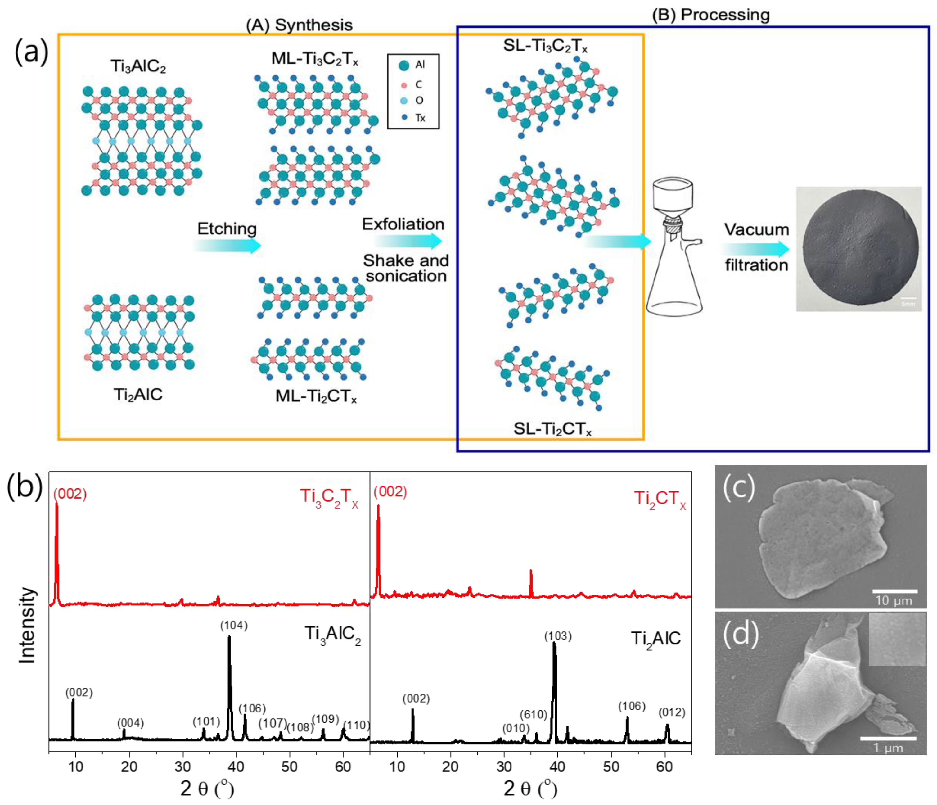
2.1. Synthesis of Ti-Based MXene and Film Preparation

The Ti-based MXenes, Ti3C2TX and Ti2CTX, were synthesized using MAX-phase Ti3AlC2 and Ti2AlC powders (37.5 μm) purchased from Suzhou Bknano Material Co., Ltd. (Suzhou, China). (Figure S1). First, 0.5 g of the MAX-phase Ti3AlC2 or Ti2AlC was slowly added to a mixture of 6 M of HCl (~37 wt% in H2O, Sigma-Aldrich, Milwaukee, St. Louis, MO, USA) and 0.5 g of LiF (≥99.0%, AR, Sigma-Aldrich, Milwaukee, America), followed by stirring at 35 °C for 24 h to etch the interlayer Al metal [27,28,29,30]. The resulting solution was transferred to a centrifuge tube, 40 mL of distilled water was added, and the mixture was centrifuged at 3500 rpm for 10 min. After the supernatant was removed, the process was repeated with 40 mL of distilled water until the solution had a pH of 6. Next, the solution was shaken for 20 min, sonicated for 5 min, and centrifuged at 3500 rpm for 10 min. After centrifugation, the supernatant was separated from the sediment to obtain the final dispersions of Ti3C2TX and Ti2CTX. The obtained dispersions were vacuum-filtered through Celgard filter paper (pore size: 64 nm) and dried at room temperature for 2 h to produce Ti3C2TX and Ti2CTX films. The prepared Ti3C2TX and Ti2CTX films were heated at a rate of 10 °C/min to 100, 200, or 300 °C in an Ar atmosphere and heat-treated for 6 h. The thickness of the Ti3C2TX and Ti2CTX films was measured using a micrometer, measured at multiple points, and then averaged.

2.2. Characterization of MXene Films

The lateral shapes of the Ti3C2TX and Ti2CTX nanoflakes and the cross-sectional structures of the Ti3C2TX and Ti2CTX films were observed using field-emission scanning electron microscopy (FE-SEM, Carl Zeiss, Merlin 3view, The Baden-württemberg Oberkorn, Germany), and the crystal structures were analyzed at room temperature using X-ray diffraction (XRD, Rigaku, Ultima IV, Tokyo, Japan). X-ray photoelectron spectroscopy (XPS, Rigaku, ZSX Primus IV, Tokyo, Japan) was used to examine the changes in the chemical bonding of Ti3C2TX and Ti2CTX materials before and after heat treatment. Ar sputtering was performed prior to the XPS analysis to eliminate the effects of surface adsorbates and oxide layers.
The sheet resistances of the Ti3C2TX and Ti2CTX films were measured using the van der Pauw method with a 4-probe setup, and the electrical conductivities were calculated by dividing the measured sheet resistances by the film thicknesses.

2.3. Measurement and Calculation of EMI Shielding Effectiveness of MXene Films

The EMI shielding effectiveness (SE) values of the Ti3C2TX and Ti2CTX films were measured using a network analyzer in the X-band frequency range (8.2–12.4 GHz). The EMI SE values were then calculated using the S-parameters with the following formulas [31,32]:
R = S 11 2 = S 22 2 T = S 12 2 = S 21 2 R + A + T = 1 S E T = S E R + S E A
S E T = 10 log 1 T = 10 log 1 S 12 2 ,
S E R = 10 log 1 1 R = 10 log 1 1 S 11 2 ,
S E A = 10 log 1 R T = 10 log 1 S 11 2 S 12 2 ,
where R, A, and T are the reflection, absorption, and transmission coefficients, respectively. SER and SEA represent the reflection and absorption SE values, respectively, and SET is the total SE. SEA implicitly includes the effectiveness from multiple internal reflections, SEM.
The EMI SE of the Ti3C2TX and Ti2CTX films at 0.5–2.0 THz was measured using a conventional terahertz time-domain spectrometer (TDS) set up with two pairs of photoconductive antennas [18,33]. The transmission through a bare substrate (undoped high-resistance silicon) was measured as a reference signal, after which Ti3C2TX and Ti2CTX films were attached to the substrate and the sample signal was recorded. The normalized transmission (EMI SE) was calculated using the following formula [34]:
E M I   S E ( d B ) = 20 l o g ( s a m p l e   s i g n a l r e f e r e n c e   s i g n a l ) .
This formula was used to determine the EMI SE values of the Ti3C2TX and Ti2CTX films.
The transfer matrix method was employed to calculate the EMI SET, SEA, and SER values of the Ti3C2TX and Ti2CTX films [31,35]. Here, we assumed a normally incident plane wave for Ti3C2TX and Ti2CTX films in air. The complex refractive index of the Ti3C2TX and Ti2CTX films was set to n = σ / 2 ω ϵ 0 1 + i because the Ti3C2TX and Ti2CTX films were conductive with high electrical conductivity, where σ is the conductivity of the Ti3C2TX or Ti2CTX film, ω is the angular frequency, and ε0 is the vacuum permittivity. The wavenumber values in vacuum (k0) and in the Ti3C2TX or Ti2CTX film (k) were k0 = ωc and k = c = k1 + ik2, respectively, where c is the speed of light in vacuum. The reflection and transmission coefficients (R and T, respectively) for the TE mode were then calculated using the transfer matrix:
T = 2 k 0 / k 0 + k 1 2 e x p 2 k 2 h , R = k 0 k 1 / k 0 + k 1 2 ,
where h is the thickness of the Ti3C2TX or Ti2CTX film. Then, SET, SER, and SEA were calculated using Equations (1), (2), and (3), respectively [31].

3. Results and Discussion

3.1. Synthesis of Ti3C2TX and Ti2CTX Nanosheets

The process of synthesizing Ti3C2TX and Ti2CTX, and preparing the films, is illustrated in Figure 1a. XRD measurements were used to confirm the synthesis of Ti3C2TX and Ti2CTX via MAX-phase etching. As shown in the XRD spectra in Figure 1b, the main peaks of Ti3AlC2 and Ti2AlC did not appear in the XRD patterns of Ti3C2TX and Ti2CTX, which indicated the complete conversion of MAX to MXene phases. The (002) characteristic peaks of Ti3C2TX and Ti2CTX were observed at 6.43° and 6.50°, corresponding to interlayer spacing values of 15.77 and 13.56 Å, respectively. The SEM images in Figure 1c,d show the synthesized Ti3C2TX and Ti2CTX nanosheets, respectively, which had measured lateral sizes of approximately 30 and 2.5 μm, respectively (Figure S2). The large difference in the lateral sizes of the Ti3C2TX and Ti2CTX nanosheets was due to the easier formation of TiO2 particles on Ti2CTX, which causes fractures throughout the nanosheet [36,37,38,39]. In fact, as shown in the SEM image in Figure 1d, the surfaces of the Ti2CTX nanosheets contained many small particles that appeared to be TiO2.

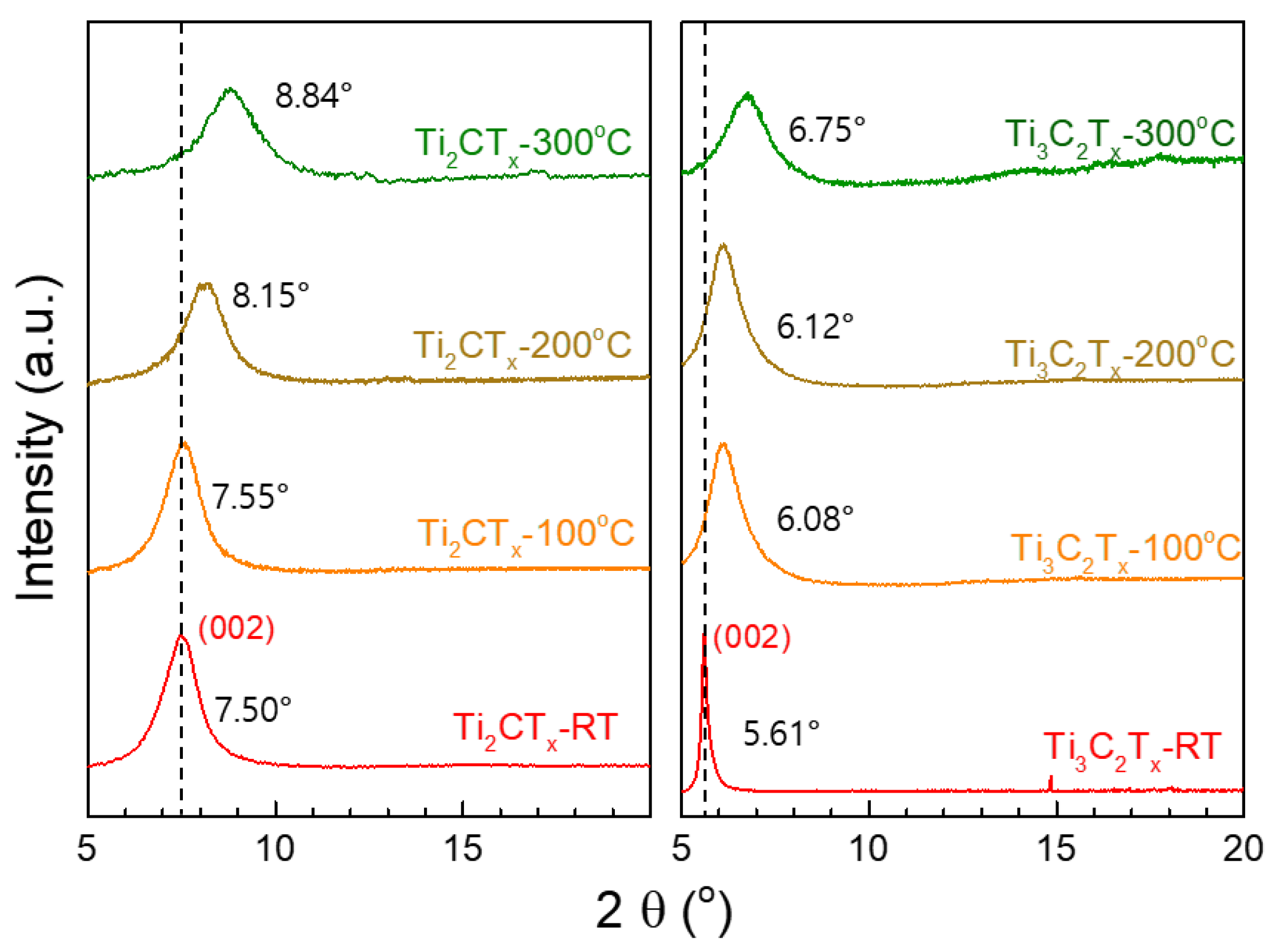
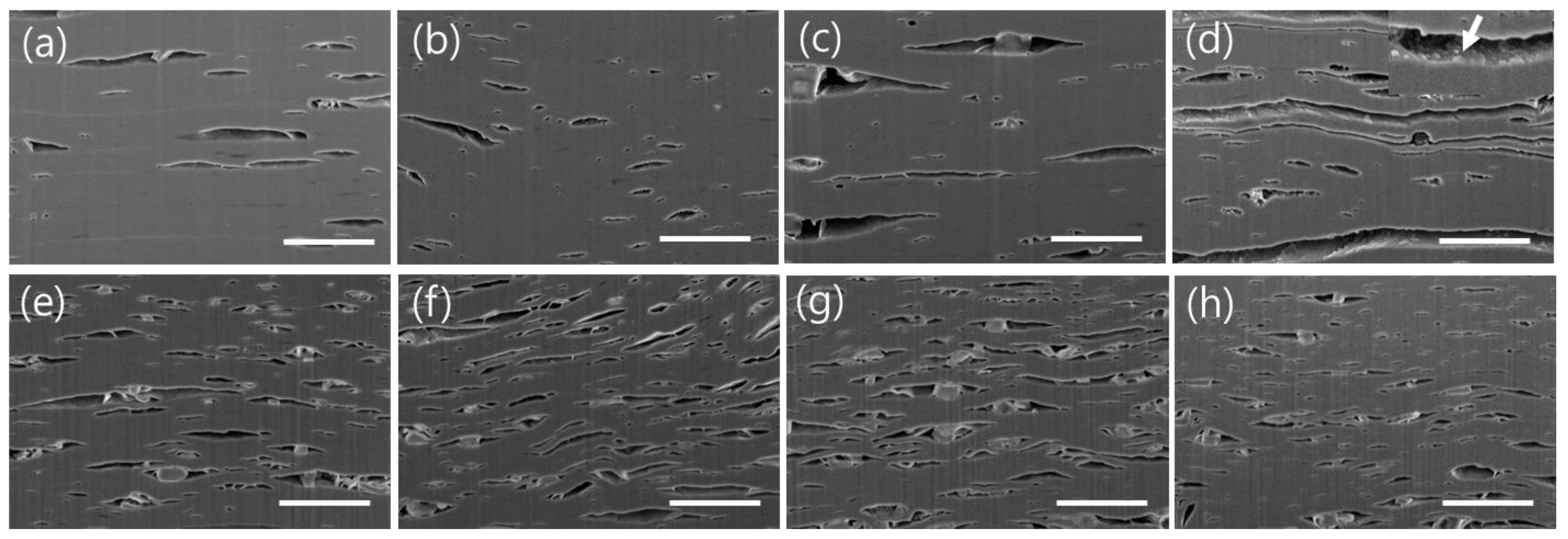
3.2. Structural Changes in Ti3C2TX and Ti2CTX Films Produced by Heat Treatment

Micrometer-thick Ti3C2TX and Ti2CTX films prepared by vacuum filtration were heat-treated at various temperatures. XRD and SEM analyses were performed to observe the microstructural changes in the Ti3C2TX and Ti2CTX films. The XRD spectra in Figure 2 show the changes in the d-spacing of (002) with the heat treatment temperature, demonstrating that the d-spacing of (002) of the Ti3C2TX and Ti2CTX films gradually decreased with increasing heat treatment temperature, as the (002) peak position shifted to the right. Table 1 lists the (002) d-spacing of the Ti3C2TX and Ti2CTX films calculated by Bragg’s law, n λ = 2 d 002 sin θ   ( λ = 1.54   ) , using the peak position in Figure 2. The d-spacing of (002) of the as-prepared Ti3C2TX film (15.75 Å) was larger than that of Ti2CTX (11.78 Å). However, the d-spacing of (002) for the two films decreased to 13.08 Å and 10.00 Å after heat treatment at 300 °C, respectively, showing similar reductions of approximately 17% and 15%, respectively.
Figure 3a–h show cross-sectional SEM images of the Ti3C2TX and Ti2CTX films before heat treatment and after heat treatment at 100, 200, and 300 °C, showing changes in the layered structure according to the heat treatment temperature. As shown in Figure 3a,e, the as-prepared Ti3C2TX and Ti2CTX films had a well-stacked layered structure of nanoflakes, but there were numerous voids of various sizes within them. In particular, Ti3C2TX contained a larger number of smaller voids. This was likely because Ti2CTX, which had a lateral size of 2 μm, formed a more densely packed layered structure compared to Ti3C2TX, which had a lateral size of approximately 30 µm, as shown in the SEM image in Figure 1c. After heat treatment, for both the Ti3C2TX and Ti2CTX films, the number of voids increased and the spacing of the interlayer gaps formed by the connected voids gradually widened with the heat treatment temperature, as shown in Figure 3a–h. The increase in voids with the heat treatment temperature was likely due to the formation of internal empty spaces resulting from the decrease in the interlayer spacing values of Ti3C2TX and Ti2CTX, as indicated by the XRD spectra in Figure 2. As shown in Figure 3a–h, the widening of the interlayer gaps owing to heat treatment was more pronounced in Ti2CTX. This was because Ti2CTX was easily oxidized when exposed to the external environment in the void regions, generating TiO2 on the surface, which further weakened the interlayer bonds and led to interlayer separation (inset of Figure 3d). In fact, large particles are occasionally observed within the film, as confirmed by the XRD spectra in Figure S3, which are presumed to be LiF particles that were not cleaned during the etching process. However, the amount of LiF is very small, as shown in the XRD spectra, so it is believed that the LiF impurities in the film do not affect the film’s properties.

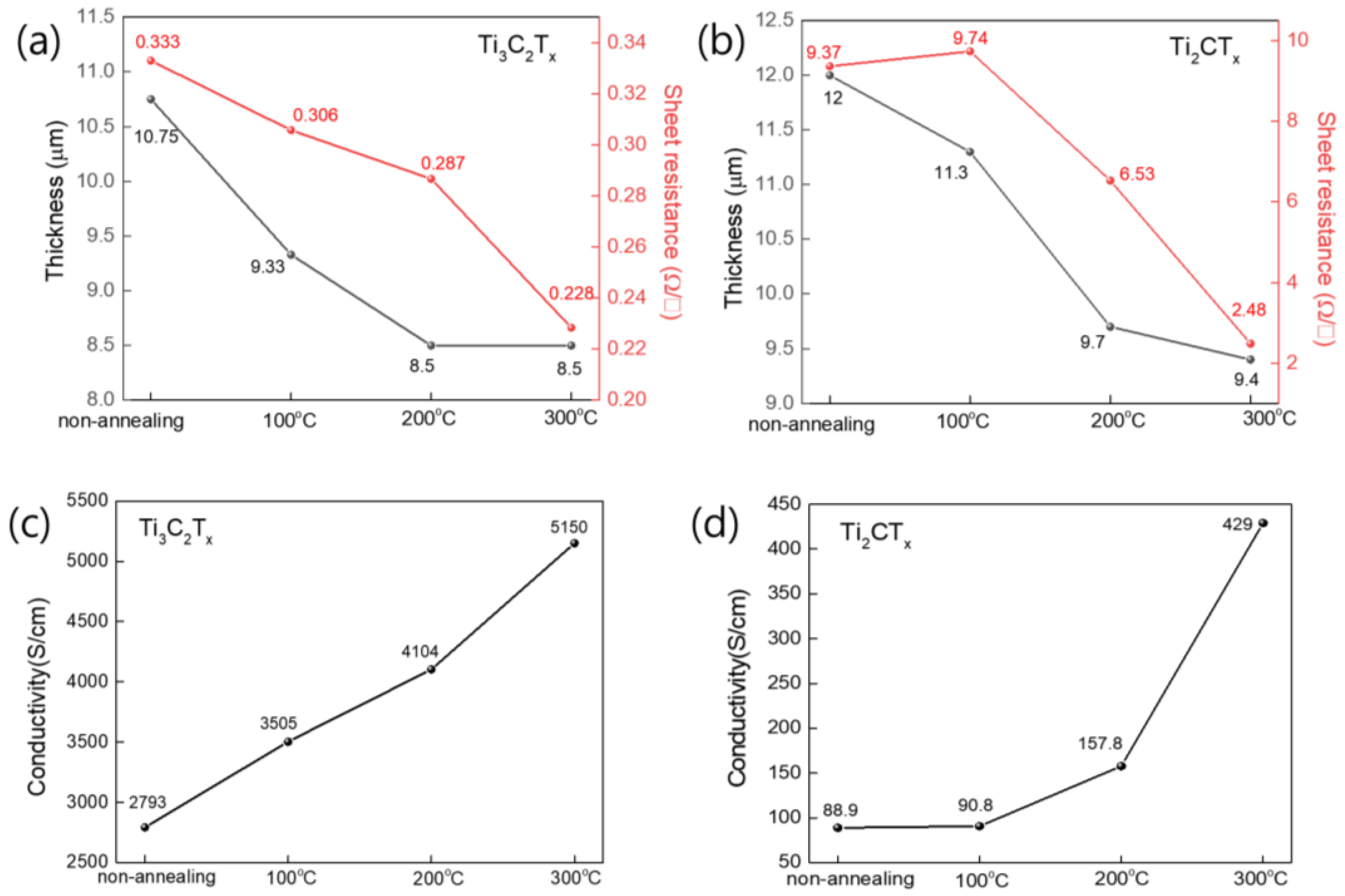
3.3. Electrical Properties of Ti3C2Tx and Ti2CTx After Heat Treatment

Figure 4a,b show the changes in the thickness and sheet resistance of the Ti3C2Tx and Ti2CTX films after heat treatment at different temperatures. These values were used to calculate the conductivities of the Ti3C2TX and Ti2CTX films, as shown in Figure 4c and Figure 4d, respectively. The thicknesses of the Ti3C2TX and Ti2CTX films decreased gradually as the heat treatment temperature increased to 200 °C, with little change after heat treatment at 300 °C. In contrast, the sheet resistances of the Ti3C2TX and Ti2CTX films decreased gradually as the heat treatment temperature increased, as shown in Figure 4b. In particular, the change in the sheet resistance of Ti2CTX with heat treatment was very large, with the sheet resistance decreasing by more than 70% from 9.37 to 2.48 Ω/sq after heat treatment at 300 °C. The sheet resistance of the Ti3C2TX film decreased from 0.33 to 0.23 Ω/sq after heat treatment at 300 °C. The conductivities of the Ti3C2TX and Ti2CTX films, which were calculated by multiplying the thickness by the sheet resistance, increased with the heat treatment temperature, as shown in Figure 4c. Overall, the conductivity of the Ti3C2TX films was significantly higher than that of the Ti2CTX films; however, the conductivity of Ti2CTX increased more rapidly than that of Ti3C2TX. The electrical conductivity of Ti3C2TX showed an increase of approximately 1.8 times, rising from 2793 S/m before heat treatment to 5150 S/cm after heat treatment at 300 °C. In contrast, Ti2CTX showed a significant increase in electrical conductivity of 4.8 times after heat treatment, from 88.9 S/cm before heat treatment to 429 S/cm after heat treatment at 300 °C. The difference in increases in the conductivities of the Ti3C2TX and Ti2CTX films with heat treatment could be attributed to the size difference between the Ti3C2TX and Ti2CTX flakes. According to the percolation theory, as the size of the flakes decreased, the increase in the contribution of interlayer transport, which had a relatively higher resistance, led to an increase in the overall resistance [40]. Moreover, the removal of the moisture and organic materials present between the layers by the heat treatment facilitated interlayer charge transport and significantly increased the conductivity [41]. Therefore, it is believed that the smaller flakes of Ti2CTX experienced a greater reduction in the resistance between flakes owing to heat treatment, resulting in a more significant change in the overall electrical conductivity.

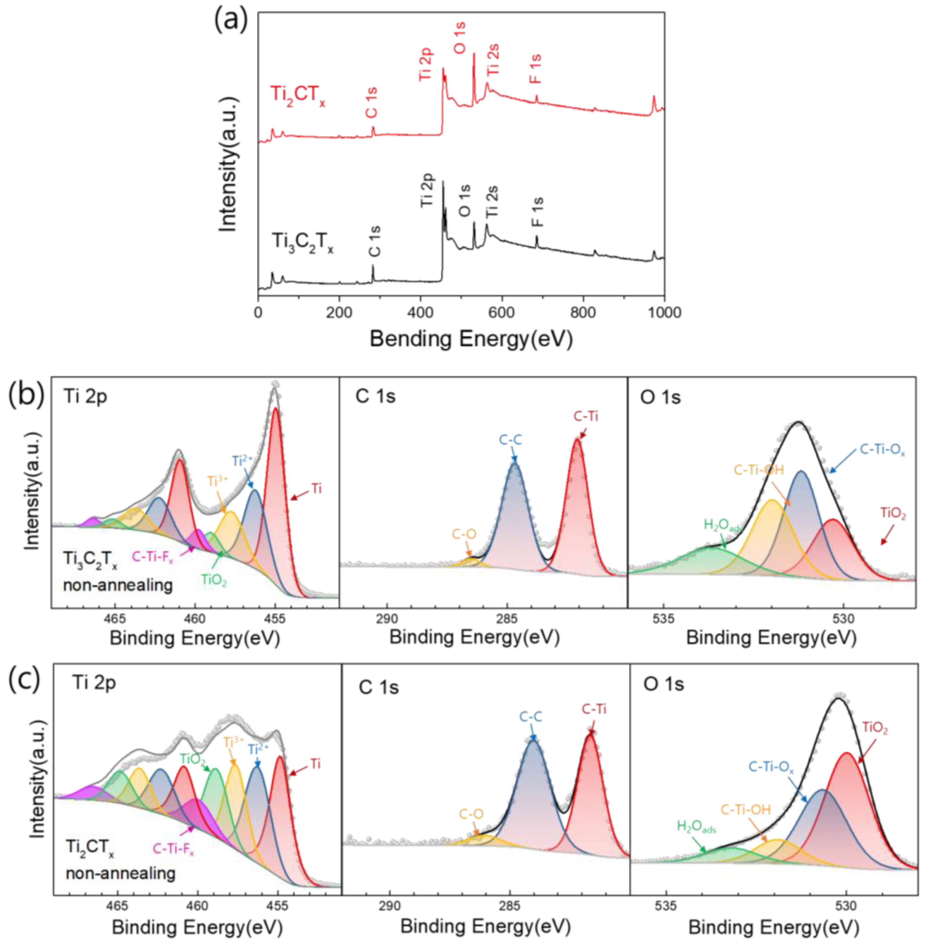
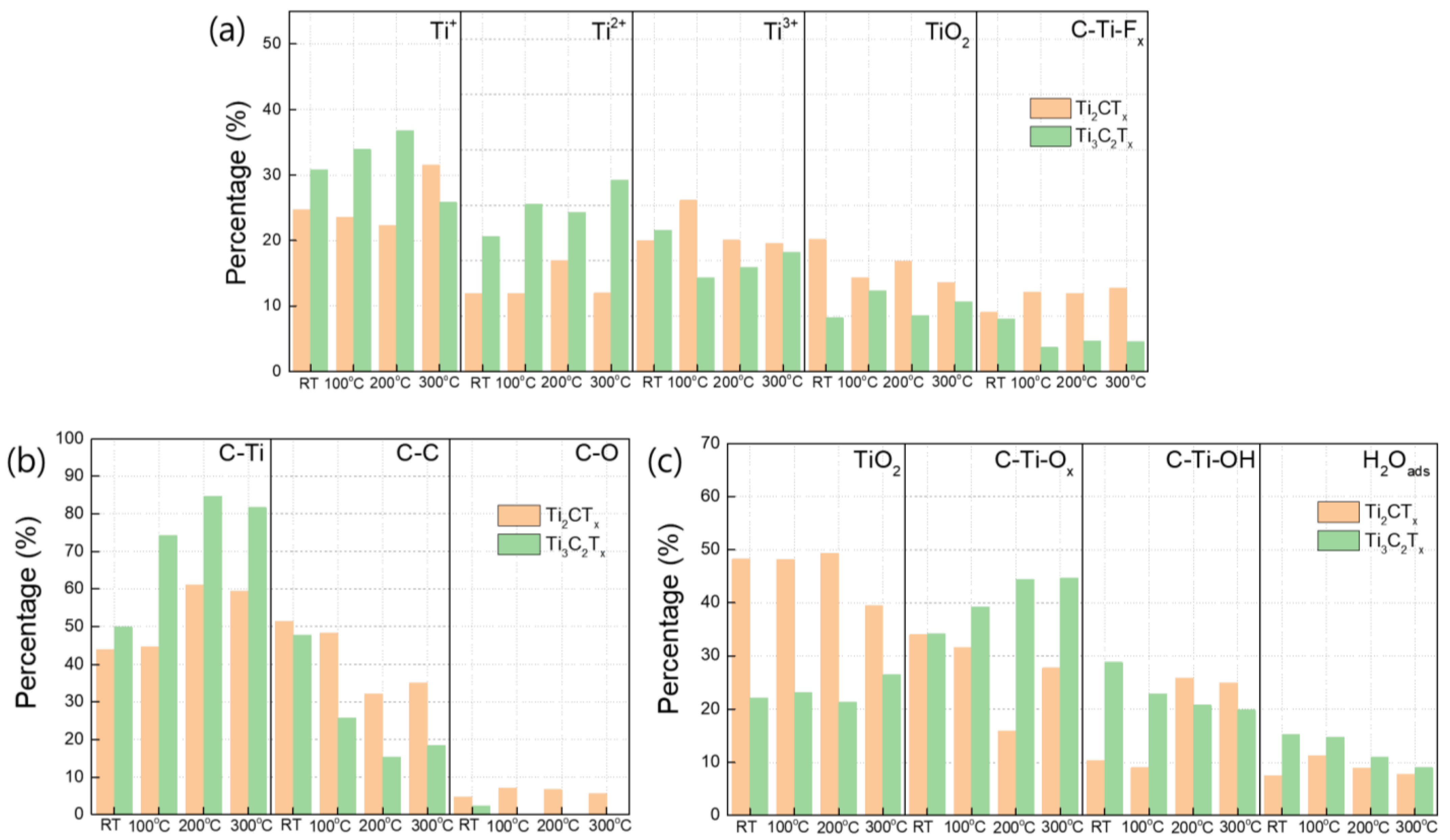
3.4. Compositional Changes in Ti3C2TX and Ti2CTX Films Produced by Heat Treatment

XPS analyses were performed to obtain information on the changes in the surface chemistry of Ti3C2TX and Ti2CTX films upon heat treatment (Figure S4). First, we compared the atomic compositions of the as-prepared Ti3C2TX and Ti2CTX from the survey spectra, and the chemical bonding of their main elements from the high-resolution XPS spectra, as shown in Figure 5a–c. Figure 5a is an XPS survey spectrum showing the composition of Ti, C, O, and F, the main elements of Ti3C2TX and Ti2CTX. It shows that Ti3C2TX had a higher number of Ti and C atoms than Ti2CTX but a lower number of O atoms. Figure 5b,c show the Ti 2p, C 1s, and O 1s XPS profiles of Ti3C2TX and Ti2CTX before annealing, respectively. The component fitting of the XPS peaks of Ti3C2TX and Ti2CTX was performed following the method outlined by Halim et al. [42]. The Ti 2p spectrum of Ti3C2TX in Figure 5b shows that the Ti peak attributed to C–Ti–O(OH) was the most dominant, and the proportion of peaks corresponding to the higher oxidation states of Ti, such as Ti2+, Ti3+, and Ti4+ (TiO2), gradually decreased. In contrast, as seen in Figure 5c, Ti2CTX had a significantly larger proportion of higher oxidation states, such as Ti2+ and Ti3+, with the Ti4+ peak corresponding to TiO2 becoming particularly prominent. These results were also observed in the O 1s spectra, where Ti3C2TX primarily showed C–Ti–OH and C–Ti–OX, whereas Ti2CTX had TiO2 as its most significant component. Meanwhile, the C 1s spectra of both Ti3C2TX and Ti2CTX exhibited a Ti–C peak at ~282 eV, corresponding to the carbon bonds located in the Ti octahedra, and a graphite-like carbon C=C peak at ~284.5 eV, originating from organic materials mainly produced during MAX etching, with both peaks occupying similar proportions in each case [43].
Figure 6a illustrates the changes in the Ti bonding state with the various heat treatment temperatures derived from the Ti 2p spectra of Ti3C2TX and Ti2CTX (Figure S5). First, as previously mentioned for Figure 5b,c, Ti3C2TX contained a larger proportion of low-oxidation-state Ti bonds, specifically Ti and Ti2+, whereas Ti2CTX had a greater proportion of Ti bonds in higher oxidation states, such as Ti3+ and Ti4+. A comparison of the changes in the Ti bonding states with the heat treatment temperature shows that the proportion of low-oxidation-state Ti and Ti2+ bonds in Ti3C2TX tended to increase, while the proportion of high-oxidation-state Ti3+ and Ti4+ bonds in Ti2CTX tended to decrease, as the heat treatment temperature increased, although there were slight deviations in the Ti bonding state of Ti3C2TX at 300 °C. The decrease in the proportion of C–C bonds with heat treatment, as shown in Figure 6b, indicates the removal of the organic materials present in Ti3C2TX and Ti2CTX with an increase in the heat treatment temperature (Figure S5). Remarkably, the removal of organic materials via heat treatment was more pronounced for Ti3C2TX than for Ti2CTX. It is also noteworthy that the C–O bonds, which are known to arise from the solvents used in the synthesis process, almost disappeared in Ti3C2TX after heat treatment, whereas in Ti2CTX, they still accounted for more than 5% and showed little change with heat treatment. An examination of the changes in the O bonding states obtained from the O 1s spectra at different heat treatment temperatures, as shown in Figure 5c, indicates that as the heat treatment temperature increased, Ti3C2TX showed a slight increase in the proportion of TiO2 and C–Ti–O bonds, whereas C–Ti–OH and H2Oads tended to gradually decrease (Figure S5). Ti2CTX, on the other hand, showed little change in the proportion of TiO2, except after heat treatment at 300 °C, but had a much higher proportion than Ti3C2TX. It is also noteworthy that the proportion of C–Ti–OH bonds increased and that H2Oads showed little change as the heat treatment temperature increased. Based on the analysis of the Ti and O bonding states, it can be concluded that both Ti3C2TX and Ti2CTX exhibited a decrease in the oxidation states of the Ti bonds owing to heat treatment. However, Ti3C2TX, which predominantly featured low-oxidation-state Ti bonds, primarily showed an increase in the proportions of Ti and Ti2+ bonds, whereas Ti2CTX, which was characterized by higher-oxidation-state Ti bonds, mainly displayed a decrease in the proportions of Ti3+ and Ti4+ bonds. Additionally, organic materials, residual solvents, and moisture adsorbed on the surface were effectively removed from Ti3C2TX by heat treatment, whereas they were less effectively removed from Ti2CTX. This difference could be attributed to the fact that, as shown in the SEM images in Figure 3a–h, Ti2CTX had a very densely stacked layered structure, whereas Ti3C2TX had a relatively porous layered structure that facilitated the removal of organic materials, moisture, and solvents.

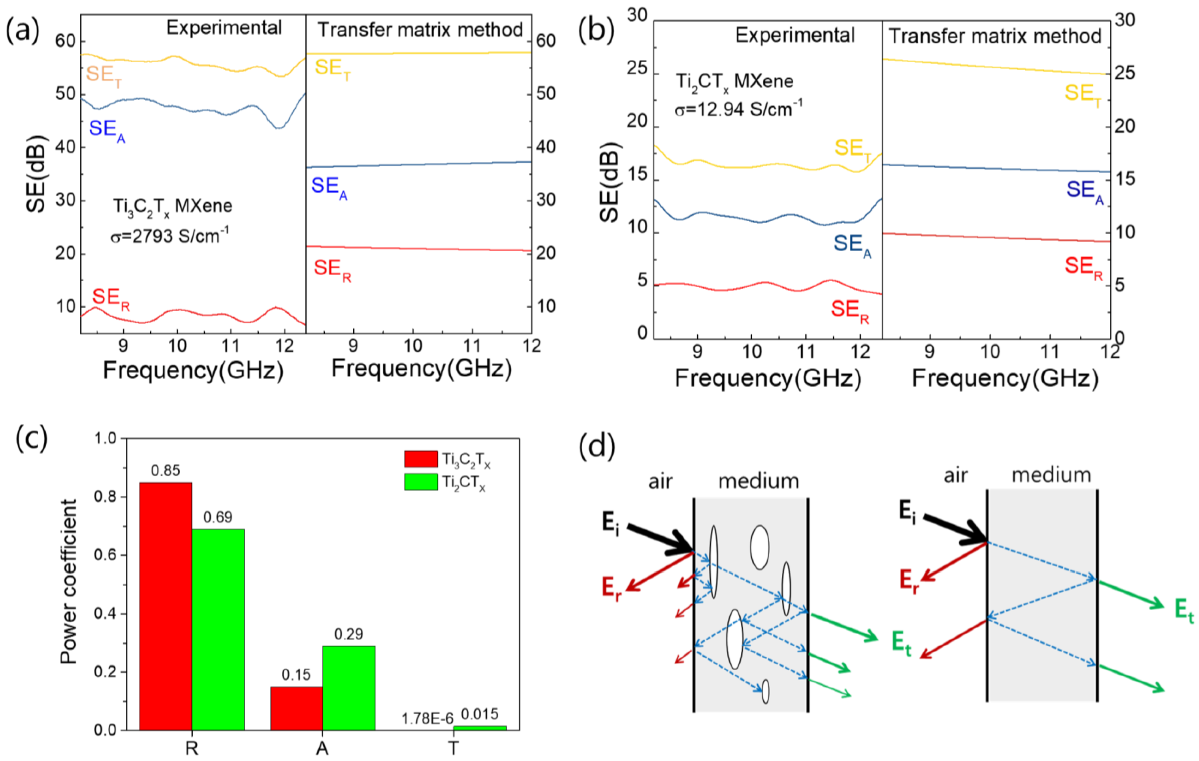
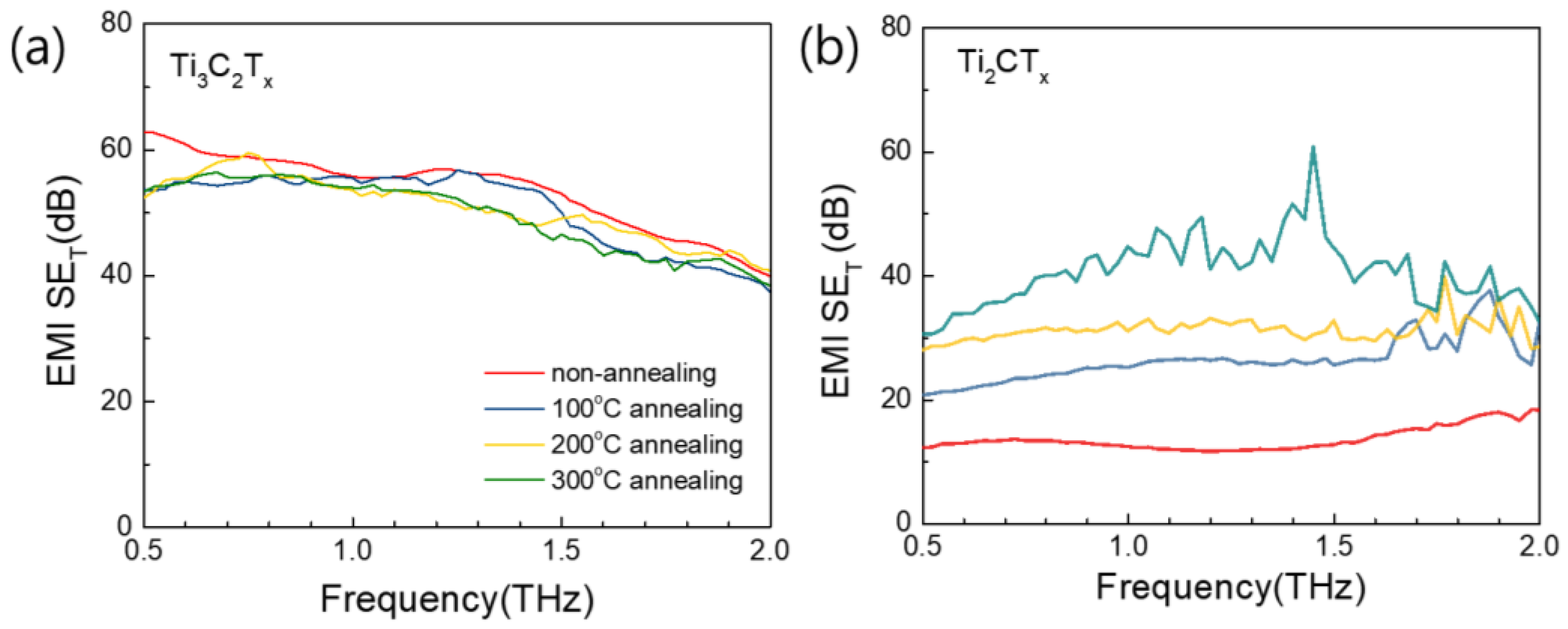
3.5. EMI Shielding Properties of Ti3C2TX and Ti2CTX Films in High-Frequency Range

Figure 7a,b show the measured EMI SE values of the as-prepared Ti3C2TX and Ti2CTX in the X-band frequency range (8.2–12.4 GHz) in comparison with the values calculated using the transfer matrix method [31]. The electrical conductivities of the Ti3C2TX and Ti2CTX films used in this experiment were 2793 and 12.94 S/cm, respectively, and their thicknesses were 10.75 and 12.05 μm, respectively. The skin depths (δ) of Ti3C2TX and Ti2CTX were calculated to be 10.55 and 59.09 μm at 8.2 GHz, respectively, based on the following formula: δ = 1 / π σ μ f , where σ, μ, and f are the conductivity, permeability, and frequency, respectively. Because the Ti2CTX film thickness of 12.05 μm was much thinner than the skin depth of 59.09 μm, we calculated EMI SE using the transfer matrix method rather than the Simon equation to include multiple reflections [30]. Figure 7a shows that the measured total EMI SE (SET) of Ti3C2TX was very close to the calculated value obtained using the transfer matrix method. However, the measured reflected EMI SE (SER) was smaller than the calculated value, while the absorbed EMI SE (SEA) was the opposite, with the measured value being larger than the calculated value. In contrast, Figure 7b shows that all the measured EMI SE (SET, SEA, SER) values of Ti2CTX were lower than the values calculated using the transfer matrix method. These results were likely due to the fact that Ti2CTX was easily oxidized in the atmosphere, resulting in a decrease in electrical conductivity over time. In practice, electromagnetic shielding is performed a few days after sample fabrication, and the electrical conductivity of Ti2CTX films typically decreases by 3% after 4 days (Figure S6) [37]. Notably, in Ti2CTX, the contributions of EA and ER to Etot were not significantly different between the experiments and calculations, unlike in Ti3C2TX. The differences appeared to be attributable to differences in the internal structures of the stacked films of Ti3C2TX and Ti2CTX. As previously discussed for Figure 3a,e, Ti3C2TX had a porous structure with many voids, whereas Ti2CTX had a relatively densely stacked structure. In order to further clarify the EMI shielding mechanism, the power coefficients of the Ti3C2TX and Ti2CTX films were calculated using Equations (1)–(3) [44]. As shown in Figure 7c, the near-zero T value of Ti3C2TX indicates that the incident electromagnetic waves hardly penetrate the Ti3C2TX film, and the reflection is still the dominant shielding mechanism in Ti3C2TX since R is higher than A. The Ti2CTX film with a T of 0.015 showed a higher A than Ti3C2TX, which indicates that the Ti2CTX film is unfavorable for the blocking of EM waves but has a higher absorption contribution to shielding than Ti3C2TX. This is not due to increased electromagnetic absorption in Ti2CTX, but rather to the low electrical conductivity of Ti2CTX, which results in less electromagnetic reflection from the surface and thus more absorption contributing to shielding. The many small TiO2 particles observed in the SEM image in Figure 3 could contribute to the increased electromagnetic absorption of the Ti2CTX film due to dielectric losses, but conversely, the oxidation of Ti2CTX could also result in decreased absorption due to decreased electrical conductivity. On the other hand, the absorption contribution to the shielding of Ti3C2TX, defined as the ratio of A to (A + R), is 0.15, which is much larger than the expected value of 0.007 from the transfer matrix method (Figure S7). This means that the absorption contribution is increased by the internal pores in the Ti3C2TX film, as already discussed in Figure 7a,b. The schematics in Figure 7d illustrate the multiple reflections that can occur in materials with and without pores in the interior; in porous materials, more absorption can occur inside the material by reflections from the surface of the pores. Therefore, Ti3C2TX, which had more internal pores, was considered to have a larger SEA than that calculated using the transfer matrix method.
Figure 8a–c show the SET, SEA, and SER values normalized to the thickness of the as-prepared Ti3C2TX and Ti3C2TX films heat-treated at 100, 200, and 300 °C, respectively. The SET of Ti3C2TX normalized to thickness (SET/t) increased with the heat treatment temperature up to 200 °C, with no significant increase after heat treatment at 300 °C. Interestingly, the SER normalized to thickness (SER/t) was almost the same for all the Ti3C2TX films heat-treated at different temperatures, despite the difference in their electrical conductivities. As previously discussed in the XPS analysis of the Ti3C2TX films heat-treated at different temperatures, the increase in the conductivity of Ti3C2TX by heat treatment was mainly caused by the removal of organic material or adsorbed solvents between the Ti3C2TX flakes and not by chemical bonding or compositional changes in Ti3C2TX. Therefore, because the electrical conductivity of the Ti3C2TX flake was hardly changed by heat treatment, SER, which was mainly caused by electromagnetic waves reflected from the surface of the Ti3C2TX film, did not seem to change significantly after heat treatment. In contrast, the SEA normalized to thickness (SEA/t) increased with the heat treatment temperature, similarly to SET/t. These results can be explained by two factors: the electrical conductivity and the porous structure. First, a sample with a higher electrical conductivity, that is, less skin depth, absorbed electromagnetic waves better for the same thickness; therefore, when the Ti3C2TX was heat-treated at higher temperatures, it had a larger SEA/t. Second, as previously discussed, the Ti3C2TX film heat-treated at higher temperatures had a more porous structure with many voids, which allowed it to absorb electromagnetic waves more efficiently through multiple reflections. In conclusion, the increase in the SET/t value of Ti3C2TX produced by heat treatment was mainly caused by the increase in absorption due to changes in the stacking structure of the Ti3C2TX flakes, not by changes in the Ti3C2TX material itself.
In fact, there have been many efforts to improve EMI shielding by fabricating composites or foams to introduce interfaces for internal scattering [45,46,47,48]. However, adding conductive nanowires or magnetic particles to the MXene film changes the electrical conductivity of the EMI shielding material, which in turn affects the reflection and absorption of EMI. Lightweight MXene foam, fabricated from MXene film through a foaming process, exhibited a significant increase in EMI SE for the same mass, but with a very large increase in thickness. In comparison, the porous MXene film prepared by a simple heat treatment method in this study exhibited an EMI SE of about 60 dB at a film thickness of about 9 μm, which was superior to MXene foam with an EMI SE of about 40 dB at the same thickness.
We also measured the electromagnetic shielding of Ti3C2TX and Ti2CTX films heat-treated at different temperatures in the THz region [33,49]. Although the difference between the Ti3C2TX films heat-treated at different temperatures could not be measured due to equipment limitations, Figure 9 shows that the electromagnetic shielding of all the Ti3C2TX samples in the 0.5–2.0 THz range was higher than that of Ti2CTX. Therefore, Ti-based MXenes, including Ti3C2TX and Ti2CTX, have high EMI SE, with values generally greater than 20 dB at frequencies higher than the GHz range, which satisfy industry application requirements for 5G technology.

4. Conclusions

In summary, we studied the EMI effectiveness of heat-treated Ti3C2TX and Ti2CTX films in the X-band frequency range and analyzed the effects of microstructural changes in the Ti3C2TX and Ti2CTX films on electromagnetic wave reflection and absorption. The Ti3C2TX film was composed of large flakes with a lateral size of tens of micrometers and had a relatively porous structure. Conversely, the Ti2CTX film, which was composed of flakes with a measured size of a few micrometers, demonstrated a more densely packed structure with minimal internal pores. After heat-treating the Ti3C2TX and Ti2CTX films at 300 °C, an analysis of the changes in their microstructures and chemical bonding revealed that the oxidation state of Ti decreased in both films; however, no significant changes in the chemical bonding of the materials themselves were observed. Nonetheless, the reduction in organic content within the Ti3C2TX film was more pronounced, which is believed to be due to the more porous internal structure of Ti3C2TX. In conclusion, the EMI electromagnetic wave absorption effectiveness of Ti3C2TX was not only higher than predicted by the transfer matrix method, but it also gradually increased with heat treatment, showing a value of approximately 6 dB per micrometer of thickness after heat treatment at 300 °C, while the electromagnetic wave reflectance remained almost unchanged. Additionally, Ti3C2TX exhibited a high EMI SE of >60 dB in the THz frequency range. Therefore, we anticipate that Ti3C2TX films made from large flakes with sizes of tens of micrometers and subjected to high-temperature heat treatment will be useful as an electromagnetic wave-shielding material, particularly for absorption across a wide range of high frequencies.

Supplementary Materials

The following supporting information can be downloaded at: https://www.mdpi.com/article/10.3390/nano15090676/s1, Figure S1. SEM images of (a–c) Ti3C2TX and (d–f) Ti2CTX flakes, comparing their lateral sizes. Figure S2. SEM images of (a) Ti2AlC and (b) Ti3AlC2 MAX powder. Figure S3. SEM images of (a) Ti2AlC and (b) Ti3AlC2 MAX powder. Figure S4. Compositional changes in the main elements (Ti, C, O, F and Cl) of Ti3C2TX and Ti2CTX upon heat treatment at different temperatures. Figure S5. High resolution XPS spectra of (a,b) Ti 2p, (c,d) C 1s, and (e,f) O 1s of Ti3C2TX and Ti2CTX upon heat treatment. Figure S6 Changes in the electrical conductivity of Ti3C2TX and Ti2CTX film over time when exposed to the atmosphere. Figure S7. (a,b) Power coefficient, R, A and T, of Ti3C2TX and Ti2CTX film calculated with SER, SEA and SET measured experimentally and calculated by transfer matrix method, respectively, using Equations (1)–(3).

Author Contributions

Conceptualization: Y.S.W.; methodology: Y.S.W. and X.H.; validation: X.H. and J.J.L.; formal analysis: X.H. and J.S.K.; investigation: Y.S.W. and X.H.; data curation: X.H., J.J.L. and J.S.K.; writing—original draft preparation: X.H.; writing—review and editing: Y.S.W.; supervision: Y.S.W. and J.S.K.; project administration: Y.S.W.; funding acquisition: Y.S.W. All authors have read and agreed to the published version of the manuscript.

Funding

This work was supported by a National Research Foundation of Korea (NRF) grant funded by the Korean Government (no. NRF-2022R1A2C2006379).

Data Availability Statement

The data presented in this study are available upon request from the corresponding author.

Conflicts of Interest

The authors declare no conflicts of interest.

References

  1. Russell, C.L. 5 G wireless telecommunications expansion: Public health and environmental implications. Environ. Res. 2018, 165, 484–495. [Google Scholar] [CrossRef]
  2. Jiang, Z.-Y.; Huang, W.; Chen, L.-S.; Liu, Y.-H. Ultrathin, lightweight, and freestanding metallic mesh for transparent elec-tromagnetic interference shielding. Opt. Express 2019, 27, 24194–24206. [Google Scholar] [CrossRef]
  3. Wan, Y.J.; Zhu, P.L.; Yu, S.H.; Sun, R.; Wong, C.P.; Liao, W.H. Anticorrosive, ultralight, and flexible carbon-wrapped metallic nanowire hybrid sponges for highly efficient electromagnetic interference shielding. Small 2018, 14, 1800534. [Google Scholar] [CrossRef]
  4. Geetha, S.; Satheesh Kumar, K.; Rao, C.R.; Vijayan, M.; Trivedi, D. EMI shielding: Methods and materials—A review. J. Appl. Polym. Sci. 2009, 112, 2073–2086. [Google Scholar] [CrossRef]
  5. Chung, D. Materials for electromagnetic interference shielding. J. Mater. Eng. Perform. 2000, 9, 350–354. [Google Scholar] [CrossRef]
  6. Chung, D. Materials for electromagnetic interference shielding. Mater. Chem. Phys. 2020, 255, 123587. [Google Scholar] [CrossRef]
  7. Wang, X.-Y.; Liao, S.-Y.; Wan, Y.-J.; Zhu, P.-L.; Hu, Y.-G.; Zhao, T.; Sun, R.; Wong, C.-P. Electromagnetic interference shielding materials: Recent progress, structure design, and future perspective. J. Mater. Chem. C 2021, 10, 44–72. [Google Scholar] [CrossRef]
  8. Li, X.; Yin, X.; Liang, S.; Li, M.; Cheng, L.; Zhang, L. 2D carbide MXene Ti2CTX as a novel high-performance electromagnetic interference shielding material. Carbon 2019, 146, 210–217. [Google Scholar] [CrossRef]
  9. Naguib, M.; Kurtoglu, M.; Presser, V.; Lu, J.; Niu, J.; Heon, M.; Hultman, L.; Gogotsi, Y.; Barsoum, M.W. Two-dimensional nanocrystals produced by exfoliation of Ti3AlC2. Adv Mater. 2011, 23, 4248–4253. [Google Scholar] [CrossRef]
  10. Jiang, Q.; Lei, Y.; Liang, H.; Xi, K.; Xia, C.; Alshareef, H.N. Review of MXene electrochemical microsupercapacitors. Energy Storage Mater. 2020, 27, 78–95. [Google Scholar] [CrossRef]
  11. Shahzad, F.; Iqbal, A.; Kim, H.; Koo, C.M. 2D Transition Metal Carbides (MXenes): Applications as an Electrically Conducting Material. Adv. Mater. 2020, 32, e2002159. [Google Scholar] [CrossRef] [PubMed]
  12. Murali, G.; Reddy Modigunta, J.K.; Park, Y.H.; Lee, J.-H.; Rawal, J.; Lee, S.-Y.; In, I.; Park, S.-J. A review on MXene synthesis, stability, and photocatalytic applications. ACS Nano 2022, 16, 13370–13429. [Google Scholar] [CrossRef]
  13. Li, X.; Huang, Z.; Shuck, C.E.; Liang, G.; Gogotsi, Y.; Zhi, C. MXene chemistry, electrochemistry and energy storage applica-tions. Nat. Rev. Chem. 2022, 6, 389–404. [Google Scholar] [CrossRef]
  14. Guo, T.; Zhou, D.; Deng, S.; Jafarpour, M.; Avaro, J.; Neels, A.; Heier, J.; Zhang, C. Rational design of Ti3C2Tx MXene inks for conductive, transparent films. ACS Nano 2023, 17, 3737–3749. [Google Scholar] [CrossRef]
  15. Shahzad, F.; Alhabeb, M.; Hatter, C.B.; Anasori, B.; Hong, S.M.; Koo, C.M.; Gogotsi, Y. Electromagnetic interference shielding with 2D transition metal carbides (MXenes). Science 2016, 353, 1137–1140. [Google Scholar] [CrossRef]
  16. Verma, R.; Thakur, P.; Chauhan, A.; Jasrotia, R.; Thakur, A. A review on MXene and its’ composites for electromagnetic interference (EMI) shielding applications. Carbon 2023, 208, 170–190. [Google Scholar] [CrossRef]
  17. Iqbal, A.; Kwon, J.; Kim, M.-K.; Koo, C. MXenes for electromagnetic interference shielding: Experimental and theoretical perspectives. Mater. Today Adv. 2021, 9, 100124. [Google Scholar] [CrossRef]
  18. Zhao, T.; Xie, P.; Wan, H.; Ding, T.; Liu, M.; Xie, J.; Li, E.; Chen, X.; Wang, T.; Zhang, Q.; et al. Ultrathin MXene assemblies approach the intrinsic absorption limit in the 0.5–10 THz band. Nat. Photonics 2023, 17, 622–628. [Google Scholar] [CrossRef]
  19. Shi, Y.; Xiang, Z.; Cai, L.; Pan, F.; Dong, Y.; Zhu, X.; Cheng, J.; Jiang, H.; Lu, W. Multi-interface Assembled N-Doped MXene/HCFG/AgNW Films for Wearable Electromagnetic Shielding Devices with Multimodal Energy Conversion and Healthcare Monitoring Performances. ACS Nano 2022, 16, 7816–7833. [Google Scholar] [CrossRef]
  20. Zhao, Y.; Miao, B.; Nawaz, M.A.; Zhu, Q.; Chen, Q.; Reina, T.R.; Bai, J.; He, D.; Al-Tahan, M.A.; Arsalan, M. Construction of cellulose nanofiber-Ti3C2Tx MXene/silver nanowire nanocomposite papers with gradient structure for efficient electromagnetic interference shielding. Adv. Compos. Hybrid Mater. 2024, 7, 1–16. [Google Scholar] [CrossRef]
  21. Zhao, S.; Zhang, H.-B.; Luo, J.-Q.; Wang, Q.-W.; Xu, B.; Hong, S.; Yu, Z.-Z. Highly electrically conductive three-dimensional Ti3C2Tx MXene/reduced graphene oxide hybrid aerogels with excellent electromagnetic interference shielding performances. ACS Nano 2018, 12, 11193–11202. [Google Scholar] [CrossRef] [PubMed]
  22. Yuan, Y.; Liu, L.; Yang, M.; Zhang, T.; Xu, F.; Lin, Z.; Ding, Y.; Wang, C.; Li, J.; Yin, W.; et al. Lightweight, thermally insulating and stiff carbon honeycomb-induced graphene composite foams with a horizontal laminated structure for electromagnetic interference shielding. Carbon 2017, 123, 223–232. [Google Scholar] [CrossRef]
  23. Liu, J.; Zhang, H.; Xie, X.; Yang, R.; Liu, Z.; Liu, Y.; Yu, Z. Multifunctional, Superelastic, and Lightweight MXene/Polyimide Aerogels. Small 2018, 14, e1802479. [Google Scholar] [CrossRef] [PubMed]
  24. Weng, G.M.; Li, J.; Alhabeb, M.; Karpovich, C.; Wang, H.; Lipton, J.; Maleski, K.; Kong, J.; Shaulsky, E.; Elimelech, M. Layer-by-layer assembly of cross-functional semi-transparent MXene-carbon nanotubes composite films for next-generation elec-tromagnetic interference shielding. Adv. Funct. Mater. 2018, 28, 1803360. [Google Scholar] [CrossRef]
  25. Zhang, Y.; Yan, Y.; Qiu, H.; Ma, Z.; Ruan, K.; Gu, J. A mini-review of MXene porous films: Preparation, mechanism and application. J. Mater. Sci. Technol. 2022, 103, 42–49. [Google Scholar] [CrossRef]
  26. Iqbal, A.; Shahzad, F.; Hantanasirisakul, K.; Kim, M.-K.; Kwon, J.; Hong, J.; Kim, D.; Gogotsi, Y.; Koo, C.M. Anomalous absorption of electromagnetic waves by 2D transition metal carbonitride Ti3CNTx (MXene). Science 2020, 369, 446–450. [Google Scholar] [CrossRef]
  27. Verger, L.; Natu, V.; Carey, M.; Barsoum, M.W. MXenes: An Introduction of Their Synthesis, Select Properties, and Applications. Trends Chem. 2019, 1, 656–669. [Google Scholar] [CrossRef]
  28. Alhabeb, M.; Maleski, K.; Anasori, B.; Lelyukh, P.; Clark, L.; Sin, S.; Gogotsi, Y. Guidelines for Synthesis and Processing of Two-Dimensional Titanium Carbide (Ti3C2Tx MXene). Chem. Mater. 2017, 29, 7633–7644. [Google Scholar] [CrossRef]
  29. Li, T.; Jabari, E.; McLellan, K.; Naguib, H.E. Review of additive manufacturing with 2D MXene: Techniques, applications, and future perspectives. Prog. Addit. Manuf. 2023, 8, 1587–1617. [Google Scholar] [CrossRef]
  30. Benchakar, M.; Loupias, L.; Garnero, C.; Bilyk, T.; Morais, C.; Canaff, C.; Guignard, N.; Morisset, S.; Pazniak, H.; Hurand, S.; et al. One MAX phase, different MXenes: A guideline to understand the crucial role of etching conditions on Ti3C2Tx surface chemistry. Appl. Surf. Sci. 2020, 530, 530. [Google Scholar] [CrossRef]
  31. Yun, T.; Kim, H.; Iqbal, A.; Cho, Y.S.; Lee, G.S.; Kim, M.; Kim, S.J.; Kim, D.; Gogotsi, Y.; Kim, S.O.; et al. Electromagnetic Shielding of Monolayer MXene Assemblies. Adv. Mater. 2020, 32, e1906769. [Google Scholar] [CrossRef] [PubMed]
  32. Li, Z.; Wang, Z.; Lu, W.; Hou, B. Theoretical Study of Electromagnetic Interference Shielding of 2D MXenes Films. Metals 2018, 8, 652. [Google Scholar] [CrossRef]
  33. Zou, Q.; Guo, W.; Zhang, L.; Yang, L.; Zhao, Z.; Liu, F.; Ye, X.; Zhang, Y.; Shi, W. MXene-based ultra-thin film for terahertz radiation shielding. Nanotechnology 2020, 31, 505710. [Google Scholar] [CrossRef] [PubMed]
  34. Iqbal, A.; Sambyal, P.; Koo, C.M. 2D MXenes for Electromagnetic Shielding: A Review. Adv. Funct. Mater. 2020, 30, 2000883. [Google Scholar] [CrossRef]
  35. Han, M.; Shuck, C.E.; Rakhmanov, R.; Parchment, D.; Anasori, B.; Koo, C.M.; Friedman, G.; Gogotsi, Y. Beyond Ti3C2Tx: MXenes for electromagnetic interference shielding. ACS Nano 2020, 14, 5008–5016. [Google Scholar] [CrossRef]
  36. Zhao, X.; Cao, H.; Coleman, B.J.; Tan, Z.; Echols, I.J.; Pentzer, E.B.; Lutkenhaus, J.L.; Radovic, M.; Green, M.J. The role of antioxidant structure in mitigating oxidation in Ti3C2Tx and Ti2CTx MXenes. Adv. Mater. Interfaces 2022, 9, 2200480. [Google Scholar] [CrossRef]
  37. Mokrushin, A.S.; Nagornov, I.A.; Gorobtsov, P.Y.; Averin, A.A.; Simonenko, T.L.; Simonenko, N.P.; Simonenko, E.P.; Kuznetsov, N.T. Effect of Ti2CTx MXene oxidation on its gas-sensitive properties. Chemosensors 2022, 11, 13. [Google Scholar] [CrossRef]
  38. Roy, C.; De, S.K.; Banerjee, P.; Pradhan, S.; Bhattacharyya, S. Investigating suitable medium for the long-duration storage of Ti2CTx MXene. J. Alloy. Compd. 2022, 938, 168471. [Google Scholar] [CrossRef]
  39. Xu, H.; Yin, X.; Li, X.; Li, M.; Zhang, L.; Cheng, L. Thermal stability and dielectric properties of 2D Ti2C MXenes via annealing under a gas mixture of Ar and H2 atmosphere. Funct. Compos. Struct. 2019, 1, 015002. [Google Scholar] [CrossRef]
  40. Xue, Q. The influence of particle shape and size on electric conductivity of metal–polymer composites. Eur. Polym. J. 2003, 40, 323–327. [Google Scholar] [CrossRef]
  41. Kumar, K.; Kim, Y.-S.; Yang, E.-H. The influence of thermal annealing to remove polymeric residue on the electronic doping and morphological characteristics of graphene. Carbon 2013, 65, 35–45. [Google Scholar] [CrossRef]
  42. Halim, J.; Cook, K.M.; Naguib, M.; Eklund, P.; Gogotsi, Y.; Rosen, J.; Barsoum, M.W. X-ray photoelectron spectroscopy of select multi-layered transition metal carbides (MXenes). Appl. Surf. Sci. 2016, 362, 406–417. [Google Scholar] [CrossRef]
  43. Näslund, L.; Persson, P.O.Å.; Rosen, J. X-ray Photoelectron Spectroscopy of Ti3AlC2, Ti3C2Tz, and TiC Provides Evidence for the Electrostatic Interaction between Laminated Layers in MAX-Phase Materials. J. Phys. Chem. C 2020, 124, 27732–27742. [Google Scholar] [CrossRef]
  44. Peng, M.; Qin, F. Clarification of basic concepts for electromagnetic interference shielding effectiveness. J. Appl. Phys. 2021, 130, 225108. [Google Scholar] [CrossRef]
  45. Zhang, H.; Wan, J.; Wu, R.; Chen, Y.; Yu, H.; Shi, S. MXenes for electromagnetic interference shielding: Insights from structural design. Carbon 2023, 218, 118716. [Google Scholar] [CrossRef]
  46. Qu, Y.; Li, X.; Wang, X.; Dai, H. Multifunctional AgNWs@MXene/AgNFs electromagnetic shielding composites for flexible and highly integrated advanced electronics. Compos. Sci. Technol. 2022, 230, 109753. [Google Scholar] [CrossRef]
  47. Huang, M.; Wang, L.; Zhao, B.; Chen, G.; Che, R. Engineering the electronic structure on MXenes via multidimensional component interlayer insertion for enhanced electromagnetic shielding. J. Mater. Sci. Technol. 2022, 138, 149–156. [Google Scholar] [CrossRef]
  48. Liu, J.; Zhang, H.; Sun, R.; Liu, Y.; Liu, Z.; Zhou, A.; Yu, Z. Hydrophobic, flexible, and lightweight MXene foams for high-performance electromagnetic-interference shielding. Adv. Mater. 2017, 29, 1702367. [Google Scholar] [CrossRef]
  49. Titova, L.V.; Li, G.; Natu, V.; Huang, S.; Shi, T.; Amer, N.; Hafez, H.A.; Hegmann, F.A.; Turchinovich, D.; Mochalin, V.; et al. 2D MXenes: Terahertz Properties and Applications. In Proceedings of the 2020 45th International Conference on Infrared, Millimeter and Terahertz Waves (IRMMW-THz), Buffalo, NY, USA, 8–13 November 2020; pp. 1–2. [Google Scholar]
Figure 1. (a) Schematic showing the synthesis process of Ti-based MXene; (b) XRD spectra of Ti3C2TX and Ti2CTX, compared with the MAX phases of Ti3AlC2 and Ti2AlC, respectively. SEM images of the synthesized (c) Ti3C2TX and (d) Ti2CTX flakes, where the inset in (d) shows a magnified SEM image of Ti2CTX with nanoparticles on the surface.
Nanomaterials 15 00676 g001
Figure 2. XRD spectra of Ti3C2TX and Ti2CTX heat-treated at different temperatures.
Nanomaterials 15 00676 g002
Figure 3. Cross-sectional SEM images of as-prepared (a) Ti3C2TX, (e) Ti2CTX films, (bd) Ti3C2TX and (fh) Ti2CTX films heat-treated at 100, 200, and 300 °C, respectively (from left to right). The scale bar is 1 μm.
Nanomaterials 15 00676 g003
Figure 4. (a,b) Plots of thickness and sheet resistance values of Ti3C2TX and Ti2CTX films heat-treated at different temperatures, respectively. (c,d) Conductivities of Ti3C2TX and Ti2CTX films calculated using the thickness and sheet resistivity values in (a) and (b), respectively.
Nanomaterials 15 00676 g004
Figure 5. (a) XPS survey spectra of Ti3C2TX and Ti2CTX. (b,c) High-resolution XPS spectra scanned over Ti 2p, C 1s, and O 1s of Ti3C2TX and Ti2CTX films, respectively, before heat treatment.
Nanomaterials 15 00676 g005
Figure 6. Histograms showing the percentage changes in the (a) Ti, (b) C, and (c) O bonding states in the Ti3C2TX and Ti2CTX films as the heat treatment temperature increased.
Nanomaterials 15 00676 g006
Figure 7. (a,b) Measured EMI SET, SEA, and SER values for Ti3C2TX and Ti2CTX films, compared to values calculated using transfer matrix method. (c) Power coefficients, R, A, and T, of Ti3C2TX and Ti2CTX films. (d) Schematic illustrating the multiple reflections of electromagnetic waves with and without pores inside a material.
Nanomaterials 15 00676 g007
Figure 8. EMI SE values normalized to thickness: (a) SET/t, (b) SER/t, and (c) SEA/t of Ti3C2TX films heat-treated at different temperatures.
Nanomaterials 15 00676 g008
Figure 9. Total EMI SE values of (a) Ti3C2TX and (b) Ti2CTX films heat-treated at different temperatures in THz frequency range.
Nanomaterials 15 00676 g009
Table 1. The d-spacing of (002) of Ti3C2TX and Ti2CTX heat-treated at different temperatures.
Heat Treatment TemperatureTi3C2TXTi2CTX
w/o11.78 Å15.75 Å
100 °C11.71 Å14.52 Å
200 °C10.85 Å14.44 Å
300 °C10.00 Å13.08 Å
Disclaimer/Publisher’s Note: The statements, opinions and data contained in all publications are solely those of the individual author(s) and contributor(s) and not of MDPI and/or the editor(s). MDPI and/or the editor(s) disclaim responsibility for any injury to people or property resulting from any ideas, methods, instructions or products referred to in the content.

