
Investigating Floating-Gate Topology Influence on van der Waals Memory Performance

Abstract

1. Introduction
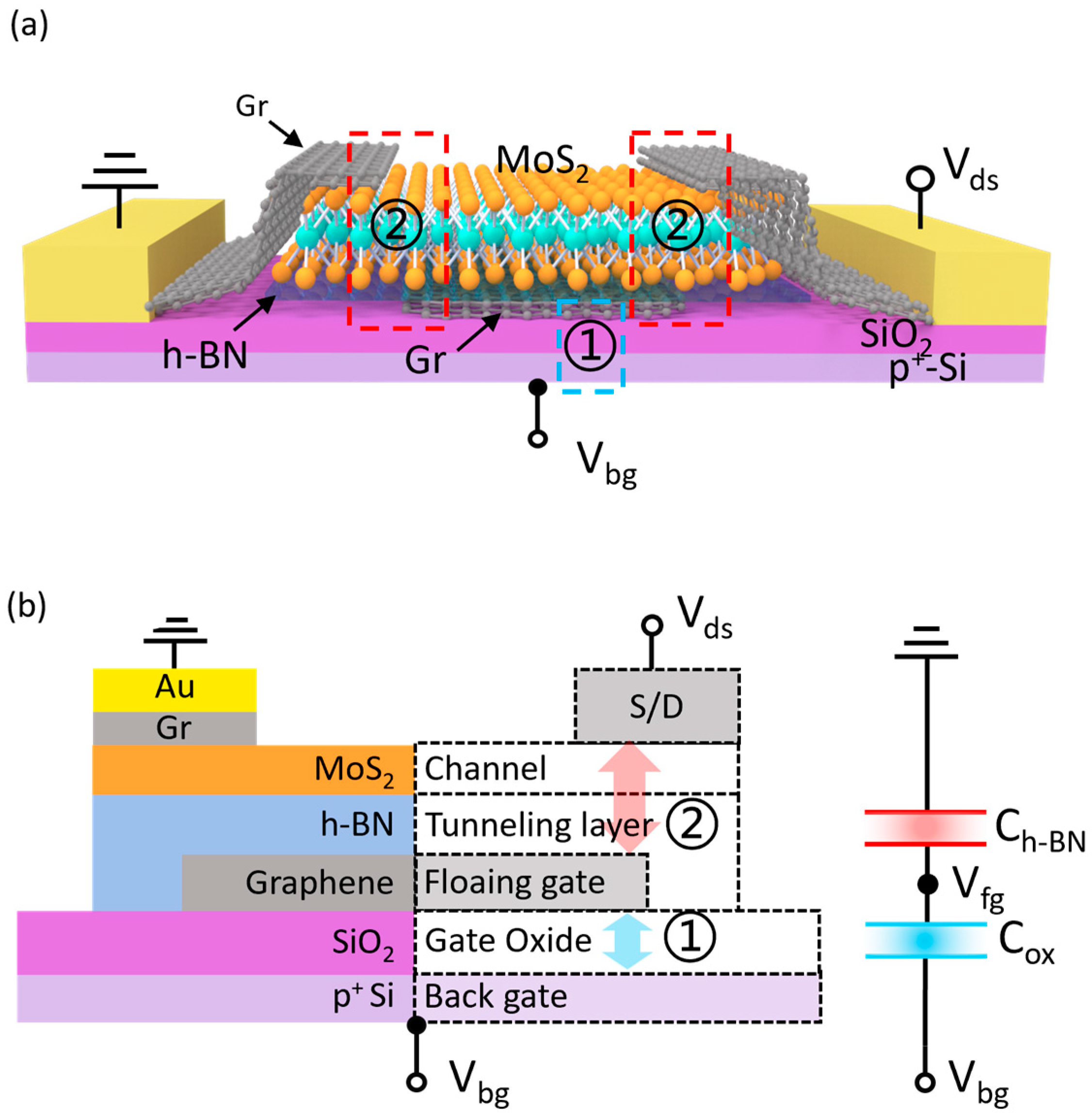
2. Experimental
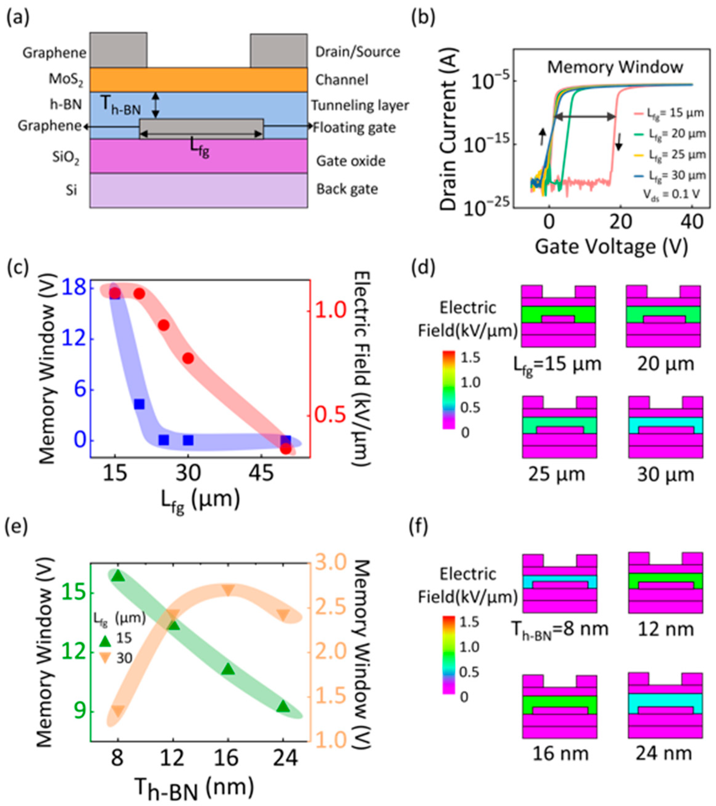
3. Results and Discussion
4. Conclusions
Supplementary Materials
Author Contributions
Funding
Data Availability Statement
Conflicts of Interest
References
- Yang, J.J.; Strukov, D.B.; Stewart, D.R. Memristive devices for computing. Nat. Nanotechnol. 2013, 8, 13–24. [Google Scholar] [CrossRef] [PubMed]
- Shulaker, M.M.; Hills, G.; Park, R.S.; Howe, R.T.; Saraswat, K.; Wong, H.-S.P.; Mitra, S. Three-dimensional integration of nanotechnologies for computing and data storage on a single chip. Nature 2017, 547, 74–78. [Google Scholar] [CrossRef]
- Intel Corporation. Micron and Intel Unveil New 3D NAND Flash Memory; Intel Newsroom: Santa Clara, CA, USA, 2015; Available online: https://www.intc.com/news-events/press-releases/detail/349/micron-and-intel-unveil-new-3d-nand-flash-memory (accessed on 10 January 2025).
- ITRS, International Technology Roadmap for Semiconductors. Flash Memory Technology Requirements (PIDS8a). 2012. Available online: https://irds.ieee.org (accessed on 10 January 2025).
- Li, M.; Lin, C.-Y.; Chang, Y.-M.; Yang, S.-H.; Lee, M.-P.; Chen, C.-F.; Lee, K.-C.; Yang, F.-S.; Lin, Y.-C.; Ueno, K.; et al. Facile and Reversible Carrier-Type Manipulation of Layered MoTe2 Toward Long-Term Stable Electronics. ACS Appl. Mater. Interfaces 2020, 12, 42918–42924. [Google Scholar] [CrossRef]
- Lee, M.-P.; Gao, C.; Tsai, M.-Y.; Lin, C.-Y.; Yang, F.-S.; Sung, H.-Y.; Zhang, C.; Li, W.; Li, J.; Zhang, J.; et al. Silicon–van der Waals heterointegration for CMOS-compatible logic-in-memory design. Sci. Adv. 2023, 9, eadk1597. [Google Scholar] [CrossRef] [PubMed]
- Liu, C.; Chen, H.; Wang, S.; Liu, Q.; Jiang, Y.-G.; Zhang, D.W.; Liu, M.; Zhou, P. Two-dimensional materials for next-generation computing technologies. Nat. Nanotechnol. 2020, 15, 545–557. [Google Scholar] [CrossRef] [PubMed]
- Zhang, P.; Cheng, N.; Li, M.; Zhou, B.; Bian, C.; Wei, Y.; Wang, X.; Jiang, H.; Bao, L.; Lin, Y.; et al. Transition-Metal Substitution-Induced Lattice Strain and Electrical Polarity Reversal in Monolayer WS2. ACS Appl. Mater. Interfaces 2020, 12, 18650–18659. [Google Scholar] [CrossRef]
- Guo, X.; Chen, H.; Bian, J.; Liao, F.; Ma, J.; Zhang, S.; Zhang, X.; Zhu, J.; Luo, C.; Zhang, Z.; et al. Stacking Monolayers at Will: A Scalable Device Optimization Strategy for Two-Dimensional Semiconductors. Nano Res. 2022, 15, 6620–6627. [Google Scholar] [CrossRef]
- Liu, C.; Yan, X.; Song, X.; Ding, S.; Zhang, D.W.; Zhou, P. A semi-floating gate memory based on van der Waals heterostructures for quasi-non-volatile applications. Nat. Nanotechnol. 2018, 13, 404–410. [Google Scholar] [CrossRef]
- Zha, J.; Shi, S.; Chaturvedi, A.; Huang, H.; Yang, P.; Yao, Y.; Li, S.; Xia, Y.; Zhang, Z.; Wang, W.; et al. Electronic/Optoelectronic Memory Device Enabled by Tellurium-based 2D van der Waals Heterostructure for in-Sensor Reservoir Computing at the Optical Communication Band. Adv. Mater. 2023, 35, 2211598. [Google Scholar] [CrossRef]
- Wu, F.; Tian, H.; Shen, Y.; Hou, Z.; Ren, J.; Gou, G.; Sun, Y.; Yang, Y.; Ren, T.-L. Vertical MoS2 transistors with sub-1-nm gate lengths. Nature 2022, 603, 259–264. [Google Scholar] [CrossRef]
- Wei, T.; Han, Z.; Zhong, X.; Xiao, Q.; Liu, T.; Xiang, D. Two dimensional semiconducting materials for ultimately scaled transistors. iScience 2022, 25, 105160. [Google Scholar] [CrossRef] [PubMed]
- Cao, W.; Khandelwal, S.; Banerjee, K. The future transistors. Nature 2023, 620, 501–515. [Google Scholar] [CrossRef]
- Vu, T.T.H.; Park, M.H.; Phan, T.L.; Park, H.J.; Vu, V.T.; Kim, H.J.; Aggarwal, P.; Won, U.Y.; Li, H.; Kim, W.K.; et al. Wafer-scale floating gate memristor array using 2D-graphene/3D-Al2O3/ZnO heterostructures for neuromorphic system. Adv. Mater. 2025, 689, 162460. [Google Scholar] [CrossRef]
- Zubair, M.; Dong, Y.; Cai, B.; Fu, X.; Wang, H.; Li, T.; Wang, J.; Liu, S.; Xia, M.; Zhao, Q.; et al. Floating gate photo-memory devices based on van der Waals heterostructures for neuromorphic image recognition. Appl. Phys. Lett. 2023, 123, 051102. [Google Scholar] [CrossRef]
- Gwon, O.H.; Kim, J.Y.; Kim, H.S.; Kang, S.; Byun, H.R.; Park, M.; Lee, D.S.; Kim, Y.; Ahn, S.; Kim, J.; et al. Systematic design and demonstration of multi-bit generation in layered materials heterostructures floating-gate memory. Adv. Funct. Mater. 2021, 31, 2105472. [Google Scholar] [CrossRef]
- Muralidharan, G.; Bhat, N.; Santhanam, V. Scalable Processes for Fabricating Non-Volatile Memory Devices Using Self-Assembled 2D Arrays of Gold Nanoparticles as Charge Storage Nodes. Nanoscale 2011, 3, 4575–4579. [Google Scholar] [CrossRef] [PubMed]
- Molina-Mendoza, A.J.; Paur, M.; Mueller, T. Nonvolatile Programmable WSe2 Photodetector. Adv. Opt. Mater. 2020, 8, 2000417. [Google Scholar] [CrossRef]
- Cho, H.; Lee, D.; Ko, K.; Lin, D.-Y.; Lee, H.; Park, S.; Park, B.; Jang, B.C.; Lim, D.-H.; Suh, J. Double-floating-gate van der Waals transistor for high-precision synaptic operations. ACS Nano 2023, 17, 7384–7393. [Google Scholar] [CrossRef]
- Kim, S.H.; Yi, S.-G.; Park, M.U.; Lee, C.; Kim, M.; Yoo, K.-H. Multilevel MoS2 optical memory with photoresponsive top floating gates. ACS Appl. Mater. Interfaces 2019, 11, 25306–25312. [Google Scholar] [CrossRef]
- Rodder, M.A.; Vasishta, S.; Dodabalapur, A. Double-gate MoS2 field-effect transistor with a multilayer graphene floating gate: A versatile device for logic, memory, and synaptic applications. ACS Appl. Mater. Interfaces 2020, 12, 33926–33933. [Google Scholar] [CrossRef]
- Sasaki, T.; Ueno, K.; Taniguchi, T.; Watanabe, K.; Nishimura, T.; Nagashio, K. Material and device structure designs for 2D memory devices based on the floating gate voltage trajectory. ACS Nano 2021, 15, 6658–6668. [Google Scholar] [CrossRef]
- Tong, L.; Wan, J.; Xiao, K.; Liu, J.; Ma, J.; Guo, X.; Zhou, L.; Chen, X.; Xia, Y.; Dai, S.; et al. Heterogeneous complementary field-effect transistors based on silicon and molybdenum disulfide. Nat. Electron. 2022, 6, 37–44. [Google Scholar] [CrossRef]
- Hong, A.J.; Song, E.B.; Yu, H.S.; Allen, M.J.; Kim, J.; Fowler, J.D.; Wassei, J.K.; Park, Y.; Wang, Y.; Zou, J.; et al. Graphene flash memory. ACS Nano 2011, 5, 7812–7817. [Google Scholar] [CrossRef] [PubMed]
- Sui, Y.; Appenzeller, J. Screening and interlayer coupling in multilayer graphene field-effect transistors. Nano Lett. 2009, 9, 2973–2977. [Google Scholar] [CrossRef] [PubMed]
- Raghunathan, S.; Krishnamohan, T.; Parat, K.; Saraswat, K.C. Investigation of ballistic current in scaled Floating-gate NAND FLASH and a solution. In Proceedings of the 2009 IEEE International Electron Devices Meeting (IEDM), Baltimore, MD, USA, 7–9 December 2009; pp. 819–822. [Google Scholar] [CrossRef]
- Dastgeer, G.; Nisar, S.; Rasheed, A.; Akbar, K.; Chavan, V.D.; Kim, D.-K.; Wabaidur, S.M.; Zulfiqar, M.W.; Eom, J. Atomically engineered, high-speed non-volatile flash memory device exhibiting multibit data storage operations. Nano Energy 2024, 119, 109106. [Google Scholar] [CrossRef]
- Gadelha, A.C.; Cadore, A.R.; Watanabe, K.; Taniguchi, T.; de Paula, A.M.; Malard, L.M.; Lacerda, R.G.; Campos, L.C. Gate-tunable non-volatile photomemory effect in MoS2 transistors. 2D Mater. 2019, 6, 025036. [Google Scholar] [CrossRef]
- Schranghamer, T.F.; Oberoi, A.; Das, S. Graphene memristive synapses for high precision neuromorphic computing. Nat. Commun. 2023, 14, 3456. [Google Scholar] [CrossRef]
- Liu, L.; Liu, C.; Jiang, L.; Li, J.; Ding, Y.; Wang, S.; Jiang, Y.-G.; Sun, Y.-B.; Wang, J.; Chen, S.; et al. Ultrafast non-volatile flash memory based on van der Waals heterostructures. Nat. Nanotechnol. 2021, 16, 874–881. [Google Scholar] [CrossRef]
- Bertolazzi, S.; Bondavalli, P.; Roche, S.; San, T.; Choi, S.; Colombo, L.; Bonaccorso, F.; Samorì, P. Nonvolatile Memories Based on Graphene and Related 2D Materials. Adv. Mater. 2019, 31, e1806663. [Google Scholar] [CrossRef]
- Belotcerkovtceva, D.; Datt, G.; Nameirakpam, H.; Aitkulova, A.; Suntornwipat, N.; Majdi, S.; Isberg, J.; Kamalakar, M.V. Extreme current density and breakdown mechanism in graphene on diamond substrate. Carbon 2025, 220, 120108. [Google Scholar] [CrossRef]
- Brzhezinskaya, M.; Kapitanova, O.; Kononenko, O.; Koveshnikov, S.; Korepanov, V.; Roshchupkin, D. Large-scalable graphene oxide films with resistive switching for non-volatile memory applications. Mater. Sci. Eng. B 2020, 262, 114345. [Google Scholar] [CrossRef]
- Shinde, P.V.; Hussain, M.; Moretti, E.; Vomiero, A. Advances in two-dimensional molybdenum ditelluride (MoTe2): A comprehensive review of properties, preparation methods, and applications. SusMat 2024, 4, e236. [Google Scholar] [CrossRef]
- Kononenko, O.; Brzhezinskaya, M.; Zotov, A.; Korepanov, V.; Levashov, V.; Matveev, V.; Roshchupkin, D. Influence of numerous Moiré superlattices on transport properties of twisted multilayer graphene. Carbon 2022, 194, 52–61. [Google Scholar] [CrossRef]
- Huang, X.; Liu, C.; Tang, Z.; Zeng, S.; Wang, S.; Zhou, P. An ultrafast bipolar flash memory for self-activated in-memory computing. Nat. Nanotechnol. 2023, 18, 486–492. [Google Scholar] [CrossRef]
- Wang, J.; Zou, X.; Xiao, X.; Xu, L.; Wang, C.; Jiang, C.; Ho, J.C.; Wang, T.; Li, J.; Liao, L. Floating Gate Memory-Based Monolayer MoS2 Transistor with Metal Nanocrystals Embedded in the Gate Dielectrics. Small 2014, 11, 208–213. [Google Scholar] [CrossRef] [PubMed]
- Wang, K.; Ling, H.; Bao, Y.; Yang, M.; Yang, Y.; Hussain, M.; Wang, H.; Zhang, L.; Xie, L.; Yi, M.; et al. A Centimeter-Scale Inorganic Nanoparticle Superlattice Monolayer with Non-Close-Packing and its High Performance in Memory Devices. Adv. Mater. 2018, 30, 1800595. [Google Scholar] [CrossRef]
- Sasaki, T.; Ueno, K.; Taniguchi, T.; Watanabe, K.; Nishimura, T.; Nagashio, K. Understanding the Memory Window Overestimation of 2D Materials Based Floating Gate Type Memory Devices by Measuring Floating Gate Voltage. Small 2020, 16, e2004907. [Google Scholar] [CrossRef]
- Cao, W.; Kang, J.; Liu, W.; Banerjee, K. A compact current–voltage model for 2D semiconductor based field-effect transistors considering interface traps, mobility degradation, and inefficient doping effect. IEEE Trans. Electron Devices 2014, 61, 4282–4290. [Google Scholar] [CrossRef]
- Hafsi, B.; Boubaker, A.; Ismaïl, N.; Kalboussi, A.; Lmimouni, K. TCAD Simulations of graphene field-effect transistors based on the quantum capacitance effect. J. Korean Phys. Soc. 2015, 67, 1201–1207. [Google Scholar] [CrossRef]
- Leenaerts, O.; Partoens, B.; Peeters, F.M.; Volodin, A.; Van Haesendonck, C. The work function of few-layer graphene. J. Phys. Condens. Matter 2016, 29, 035003. [Google Scholar] [CrossRef]
- Nathawat, J.; Zhao, M.; Kwan, C.-P.; Yin, S.; Arabchigavkani, N.; Randle, M.; Ramamoorthy, H.; He, G.; Somphonsane, R.; Matsumoto, N.; et al. Transient Response of h-BN-Encapsulated Graphene Transistors: Signatures of Self-Heating and Hot-Carrier Trapping. ACS Omega 2019, 4, 4082–4090. [Google Scholar] [CrossRef] [PubMed]
- Lopez-Sanchez, O.; Lembke, D.; Kayci, M.; Radenovic, A.; Kis, A. Ultrasensitive photodetectors based on monolayer MoS2. Nat. Nanotechnol. 2013, 8, 497–501. [Google Scholar] [CrossRef] [PubMed]
- Shi, N.; Zhang, J.; Ding, Z.; Jiang, H.; Yan, Y.; Gu, D.; Li, W.; Yi, M.; Huang, F.; Chen, S.; et al. Ultrathin Metal–Organic Framework Nanosheets as Nano-Floating-Gate for High Performance Transistor Memory Device. Adv. Funct. Mater. 2021, 32, 2110784. [Google Scholar] [CrossRef]
- Kim, T.; Kang, D.; Lee, Y.; Hong, S.; Shin, H.G.; Bae, H.; Yi, Y.; Kim, K.; Im, S. 2D TMD Channel Transistors with ZnO Nanowire Gate for Extended Nonvolatile Memory Applications. Adv. Funct. Mater. 2020, 30, 2004140. [Google Scholar] [CrossRef]
- Gong, F.; Luo, W.; Wang, J.; Wang, P.; Fang, H.; Zheng, D.; Guo, N.; Wang, J.; Luo, M.; Ho, J.C.; et al. High-Sensitivity Floating-Gate Phototransistors Based on WS2 and MoS2. Adv. Funct. Mater. 2016, 26, 6084–6090. [Google Scholar] [CrossRef]
- Gong, X.; Zhou, Y.; Xia, J.; Zhang, L.; Zhang, L.; Yin, L.-J.; Hu, Y.; Qin, Z.; Tian, Y. Tunable non-volatile memories based on 2D InSe/h-BN/GaSe heterostructures towards potential multifunctionality. Nanoscale 2023, 15, 14448–14457. [Google Scholar] [CrossRef] [PubMed]
- Wang, X.; Zhu, C.; Deng, Y.; Duan, R.; Chen, J.; Zeng, Q.; Zhou, J.; Fu, Q.; You, L.; Liu, S.; et al. Van der Waals engineering of ferroelectric heterostructures for long-retention memory. Nat. Commun. 2021, 12, 1109. [Google Scholar] [CrossRef]
- Wen, J.; Tang, W.; Kang, Z.; Liao, Q.; Hong, M.; Du, J.; Zhang, X.; Yu, H.; Si, H.; Zhang, Z.; et al. Direct Charge Trapping Multilevel Memory with Graphdiyne/MoS2 Van der Waals Heterostructure. Adv. Sci. 2021, 8, 2101417. [Google Scholar] [CrossRef]
- Zha, J.; Xia, Y.; Shi, S.; Huang, H.; Li, S.; Qian, C.; Wang, H.; Yang, P.; Zhang, Z.; Meng, Y.; et al. A 2D Heterostructure-Based Multifunctional Floating Gate Memory Device for Multimodal Reservoir Computing. Adv. Mater. 2023, 36, e2308502. [Google Scholar] [CrossRef]


| Material | Dopant Thickness | Value |
|---|---|---|
| MoS2 | Eg (eV) | 1.9 |
| εr | 4.2 | |
| χ (eV) | 4.7 | |
| μn (cm2/(V·s)) | 200 | |
| μp (cm2/(V·s)) | 76 | |
| Gr | Eg (eV) | 0 |
| εr | 25 | |
| χ (eV) | 4 | |
| gc (E) | 3 × 10¹⁷ | |
| gv (E) | 3 × 10¹⁷ | |
| μn (cm2/(V·s)) | 1 × 10⁴ | |
| μp (cm2/(V·s)) | 1 × 10⁴ | |
| h-BN | Eg (eV) | 4 |
| εr | 7.5 |
Disclaimer/Publisher’s Note: The statements, opinions and data contained in all publications are solely those of the individual author(s) and contributor(s) and not of MDPI and/or the editor(s). MDPI and/or the editor(s) disclaim responsibility for any injury to people or property resulting from any ideas, methods, instructions or products referred to in the content. |
© 2025 by the authors. Licensee MDPI, Basel, Switzerland. This article is an open access article distributed under the terms and conditions of the Creative Commons Attribution (CC BY) license (https://creativecommons.org/licenses/by/4.0/).
Share and Cite
Zheng, H.; Qin, Y.; Gao, C.; Fang, J.; Zou, Y.; Li, M.; Zhang, J. Investigating Floating-Gate Topology Influence on van der Waals Memory Performance. Nanomaterials 2025, 15, 666. https://doi.org/10.3390/nano15090666
Zheng H, Qin Y, Gao C, Fang J, Zou Y, Li M, Zhang J. Investigating Floating-Gate Topology Influence on van der Waals Memory Performance. Nanomaterials. 2025; 15(9):666. https://doi.org/10.3390/nano15090666
Chicago/Turabian StyleZheng, Hao, Yusang Qin, Caifang Gao, Junyi Fang, Yifeng Zou, Mengjiao Li, and Jianhua Zhang. 2025. "Investigating Floating-Gate Topology Influence on van der Waals Memory Performance" Nanomaterials 15, no. 9: 666. https://doi.org/10.3390/nano15090666
APA StyleZheng, H., Qin, Y., Gao, C., Fang, J., Zou, Y., Li, M., & Zhang, J. (2025). Investigating Floating-Gate Topology Influence on van der Waals Memory Performance. Nanomaterials, 15(9), 666. https://doi.org/10.3390/nano15090666